EP1032949B1 - Composant a semi-conducteur, notamment pile solaire et procede permettant de l'obtenir - Google Patents
Composant a semi-conducteur, notamment pile solaire et procede permettant de l'obtenir Download PDFInfo
- Publication number
- EP1032949B1 EP1032949B1 EP98948658A EP98948658A EP1032949B1 EP 1032949 B1 EP1032949 B1 EP 1032949B1 EP 98948658 A EP98948658 A EP 98948658A EP 98948658 A EP98948658 A EP 98948658A EP 1032949 B1 EP1032949 B1 EP 1032949B1
- Authority
- EP
- European Patent Office
- Prior art keywords
- pyrite
- accordance
- semiconductor component
- semiconductor
- base material
- Prior art date
- Legal status (The legal status is an assumption and is not a legal conclusion. Google has not performed a legal analysis and makes no representation as to the accuracy of the status listed.)
- Expired - Lifetime
Links
- 239000004065 semiconductor Substances 0.000 title claims abstract description 79
- 238000000034 method Methods 0.000 title claims description 26
- 238000004519 manufacturing process Methods 0.000 title description 8
- NIFIFKQPDTWWGU-UHFFFAOYSA-N pyrite Chemical compound [Fe+2].[S-][S-] NIFIFKQPDTWWGU-UHFFFAOYSA-N 0.000 claims abstract description 64
- 229910052683 pyrite Inorganic materials 0.000 claims abstract description 63
- 239000011028 pyrite Substances 0.000 claims abstract description 58
- 239000000463 material Substances 0.000 claims abstract description 55
- ZOXJGFHDIHLPTG-UHFFFAOYSA-N Boron Chemical compound [B] ZOXJGFHDIHLPTG-UHFFFAOYSA-N 0.000 claims abstract description 18
- OAICVXFJPJFONN-UHFFFAOYSA-N Phosphorus Chemical compound [P] OAICVXFJPJFONN-UHFFFAOYSA-N 0.000 claims abstract description 18
- 229910052796 boron Inorganic materials 0.000 claims abstract description 16
- 239000011574 phosphorus Substances 0.000 claims abstract description 16
- 229910052698 phosphorus Inorganic materials 0.000 claims abstract description 16
- 239000000203 mixture Substances 0.000 claims abstract description 10
- 239000000126 substance Substances 0.000 claims abstract description 10
- 229910052960 marcasite Inorganic materials 0.000 claims abstract 5
- XEEYBQQBJWHFJM-UHFFFAOYSA-N Iron Chemical compound [Fe] XEEYBQQBJWHFJM-UHFFFAOYSA-N 0.000 claims description 24
- 239000013078 crystal Substances 0.000 claims description 15
- 229910052742 iron Inorganic materials 0.000 claims description 10
- NINIDFKCEFEMDL-UHFFFAOYSA-N Sulfur Chemical compound [S] NINIDFKCEFEMDL-UHFFFAOYSA-N 0.000 claims description 8
- 239000010409 thin film Substances 0.000 claims description 5
- 238000004140 cleaning Methods 0.000 claims description 3
- 238000002488 metal-organic chemical vapour deposition Methods 0.000 claims description 3
- 238000005546 reactive sputtering Methods 0.000 claims description 2
- 238000005118 spray pyrolysis Methods 0.000 claims description 2
- BHEPBYXIRTUNPN-UHFFFAOYSA-N hydridophosphorus(.) (triplet) Chemical compound [PH] BHEPBYXIRTUNPN-UHFFFAOYSA-N 0.000 claims 3
- 239000005864 Sulphur Substances 0.000 claims 2
- 239000007792 gaseous phase Substances 0.000 claims 2
- 229910021577 Iron(II) chloride Inorganic materials 0.000 claims 1
- 238000001027 hydrothermal synthesis Methods 0.000 claims 1
- NMCUIPGRVMDVDB-UHFFFAOYSA-L iron dichloride Chemical compound Cl[Fe]Cl NMCUIPGRVMDVDB-UHFFFAOYSA-L 0.000 claims 1
- XSOKHXFFCGXDJZ-UHFFFAOYSA-N telluride(2-) Chemical compound [Te-2] XSOKHXFFCGXDJZ-UHFFFAOYSA-N 0.000 claims 1
- 239000006163 transport media Substances 0.000 claims 1
- 238000007704 wet chemistry method Methods 0.000 claims 1
- 239000010410 layer Substances 0.000 description 35
- 210000004027 cell Anatomy 0.000 description 31
- 229910052717 sulfur Inorganic materials 0.000 description 7
- 239000004020 conductor Substances 0.000 description 5
- 239000011593 sulfur Substances 0.000 description 5
- 230000008020 evaporation Effects 0.000 description 4
- 238000001704 evaporation Methods 0.000 description 4
- XUIMIQQOPSSXEZ-UHFFFAOYSA-N Silicon Chemical compound [Si] XUIMIQQOPSSXEZ-UHFFFAOYSA-N 0.000 description 3
- 239000002800 charge carrier Substances 0.000 description 3
- 239000012535 impurity Substances 0.000 description 3
- 239000003446 ligand Substances 0.000 description 3
- 238000001451 molecular beam epitaxy Methods 0.000 description 3
- 229910052710 silicon Inorganic materials 0.000 description 3
- 239000010703 silicon Substances 0.000 description 3
- XKRFYHLGVUSROY-UHFFFAOYSA-N Argon Chemical compound [Ar] XKRFYHLGVUSROY-UHFFFAOYSA-N 0.000 description 2
- 238000010521 absorption reaction Methods 0.000 description 2
- 239000000460 chlorine Substances 0.000 description 2
- 238000000407 epitaxy Methods 0.000 description 2
- 239000007789 gas Substances 0.000 description 2
- 238000010438 heat treatment Methods 0.000 description 2
- 238000005468 ion implantation Methods 0.000 description 2
- 239000011572 manganese Substances 0.000 description 2
- 210000002381 plasma Anatomy 0.000 description 2
- 239000000843 powder Substances 0.000 description 2
- 238000002360 preparation method Methods 0.000 description 2
- 239000007858 starting material Substances 0.000 description 2
- 238000007740 vapor deposition Methods 0.000 description 2
- WUPHOULIZUERAE-UHFFFAOYSA-N 3-(oxolan-2-yl)propanoic acid Chemical compound OC(=O)CCC1CCCO1 WUPHOULIZUERAE-UHFFFAOYSA-N 0.000 description 1
- MARUHZGHZWCEQU-UHFFFAOYSA-N 5-phenyl-2h-tetrazole Chemical compound C1=CC=CC=C1C1=NNN=N1 MARUHZGHZWCEQU-UHFFFAOYSA-N 0.000 description 1
- JBRZTFJDHDCESZ-UHFFFAOYSA-N AsGa Chemical compound [As]#[Ga] JBRZTFJDHDCESZ-UHFFFAOYSA-N 0.000 description 1
- 229910014265 BrCl Inorganic materials 0.000 description 1
- 229910001369 Brass Inorganic materials 0.000 description 1
- WKBOTKDWSSQWDR-UHFFFAOYSA-N Bromine atom Chemical compound [Br] WKBOTKDWSSQWDR-UHFFFAOYSA-N 0.000 description 1
- ZAMOUSCENKQFHK-UHFFFAOYSA-N Chlorine atom Chemical compound [Cl] ZAMOUSCENKQFHK-UHFFFAOYSA-N 0.000 description 1
- MBMLMWLHJBBADN-UHFFFAOYSA-N Ferrous sulfide Chemical compound [Fe]=S MBMLMWLHJBBADN-UHFFFAOYSA-N 0.000 description 1
- GYHNNYVSQQEPJS-UHFFFAOYSA-N Gallium Chemical compound [Ga] GYHNNYVSQQEPJS-UHFFFAOYSA-N 0.000 description 1
- 229910001218 Gallium arsenide Inorganic materials 0.000 description 1
- 102000005298 Iron-Sulfur Proteins Human genes 0.000 description 1
- 108010081409 Iron-Sulfur Proteins Proteins 0.000 description 1
- PWHULOQIROXLJO-UHFFFAOYSA-N Manganese Chemical compound [Mn] PWHULOQIROXLJO-UHFFFAOYSA-N 0.000 description 1
- UCKMPCXJQFINFW-UHFFFAOYSA-N Sulphide Chemical compound [S-2] UCKMPCXJQFINFW-UHFFFAOYSA-N 0.000 description 1
- AZOWAFFTOUGEDU-UHFFFAOYSA-N [Ar].[S] Chemical compound [Ar].[S] AZOWAFFTOUGEDU-UHFFFAOYSA-N 0.000 description 1
- 238000005263 ab initio calculation Methods 0.000 description 1
- 229910052786 argon Inorganic materials 0.000 description 1
- 229910052785 arsenic Inorganic materials 0.000 description 1
- RQNWIZPPADIBDY-UHFFFAOYSA-N arsenic atom Chemical compound [As] RQNWIZPPADIBDY-UHFFFAOYSA-N 0.000 description 1
- 230000015572 biosynthetic process Effects 0.000 description 1
- 239000010951 brass Substances 0.000 description 1
- GDTBXPJZTBHREO-UHFFFAOYSA-N bromine Substances BrBr GDTBXPJZTBHREO-UHFFFAOYSA-N 0.000 description 1
- CODNYICXDISAEA-UHFFFAOYSA-N bromine monochloride Chemical compound BrCl CODNYICXDISAEA-UHFFFAOYSA-N 0.000 description 1
- 229910052794 bromium Inorganic materials 0.000 description 1
- 229910052980 cadmium sulfide Inorganic materials 0.000 description 1
- 239000000919 ceramic Substances 0.000 description 1
- 238000006243 chemical reaction Methods 0.000 description 1
- 229910052801 chlorine Inorganic materials 0.000 description 1
- 229910017052 cobalt Inorganic materials 0.000 description 1
- 239000010941 cobalt Substances 0.000 description 1
- GUTLYIVDDKVIGB-UHFFFAOYSA-N cobalt atom Chemical compound [Co] GUTLYIVDDKVIGB-UHFFFAOYSA-N 0.000 description 1
- 238000013329 compounding Methods 0.000 description 1
- 150000001875 compounds Chemical class 0.000 description 1
- OMZSGWSJDCOLKM-UHFFFAOYSA-N copper(II) sulfide Chemical compound [S-2].[Cu+2] OMZSGWSJDCOLKM-UHFFFAOYSA-N 0.000 description 1
- 238000009792 diffusion process Methods 0.000 description 1
- 239000002019 doping agent Substances 0.000 description 1
- 230000007613 environmental effect Effects 0.000 description 1
- 230000002349 favourable effect Effects 0.000 description 1
- 239000010408 film Substances 0.000 description 1
- 229910052733 gallium Inorganic materials 0.000 description 1
- 239000011521 glass Substances 0.000 description 1
- 238000000097 high energy electron diffraction Methods 0.000 description 1
- 238000002513 implantation Methods 0.000 description 1
- 238000009434 installation Methods 0.000 description 1
- 239000012212 insulator Substances 0.000 description 1
- 229910000339 iron disulfide Inorganic materials 0.000 description 1
- 229910052748 manganese Inorganic materials 0.000 description 1
- 238000005259 measurement Methods 0.000 description 1
- 229910052751 metal Inorganic materials 0.000 description 1
- 239000002184 metal Substances 0.000 description 1
- 238000002156 mixing Methods 0.000 description 1
- 239000005445 natural material Substances 0.000 description 1
- 150000002902 organometallic compounds Chemical class 0.000 description 1
- 239000002245 particle Substances 0.000 description 1
- 230000035515 penetration Effects 0.000 description 1
- 231100000289 photo-effect Toxicity 0.000 description 1
- 230000005610 quantum mechanics Effects 0.000 description 1
- 230000005855 radiation Effects 0.000 description 1
- 238000001552 radio frequency sputter deposition Methods 0.000 description 1
- 238000002128 reflection high energy electron diffraction Methods 0.000 description 1
- 239000011347 resin Substances 0.000 description 1
- 229920005989 resin Polymers 0.000 description 1
- 239000011435 rock Substances 0.000 description 1
- 239000002356 single layer Substances 0.000 description 1
- 239000011734 sodium Substances 0.000 description 1
- 229910052708 sodium Inorganic materials 0.000 description 1
- HYHCSLBZRBJJCH-UHFFFAOYSA-N sodium polysulfide Chemical compound [Na+].S HYHCSLBZRBJJCH-UHFFFAOYSA-N 0.000 description 1
- 239000007787 solid Substances 0.000 description 1
- 238000001228 spectrum Methods 0.000 description 1
- 238000004544 sputter deposition Methods 0.000 description 1
- 239000000758 substrate Substances 0.000 description 1
- 229910052714 tellurium Inorganic materials 0.000 description 1
- PORWMNRCUJJQNO-UHFFFAOYSA-N tellurium atom Chemical compound [Te] PORWMNRCUJJQNO-UHFFFAOYSA-N 0.000 description 1
- 238000002207 thermal evaporation Methods 0.000 description 1
- 238000007669 thermal treatment Methods 0.000 description 1
- 239000012780 transparent material Substances 0.000 description 1
- 238000005019 vapor deposition process Methods 0.000 description 1
- XLYOFNOQVPJJNP-UHFFFAOYSA-N water Substances O XLYOFNOQVPJJNP-UHFFFAOYSA-N 0.000 description 1
Images
Classifications
-
- H—ELECTRICITY
- H10—SEMICONDUCTOR DEVICES; ELECTRIC SOLID-STATE DEVICES NOT OTHERWISE PROVIDED FOR
- H10F—INORGANIC SEMICONDUCTOR DEVICES SENSITIVE TO INFRARED RADIATION, LIGHT, ELECTROMAGNETIC RADIATION OF SHORTER WAVELENGTH OR CORPUSCULAR RADIATION
- H10F10/00—Individual photovoltaic cells, e.g. solar cells
-
- H—ELECTRICITY
- H10—SEMICONDUCTOR DEVICES; ELECTRIC SOLID-STATE DEVICES NOT OTHERWISE PROVIDED FOR
- H10F—INORGANIC SEMICONDUCTOR DEVICES SENSITIVE TO INFRARED RADIATION, LIGHT, ELECTROMAGNETIC RADIATION OF SHORTER WAVELENGTH OR CORPUSCULAR RADIATION
- H10F77/00—Constructional details of devices covered by this subclass
- H10F77/10—Semiconductor bodies
- H10F77/12—Active materials
-
- H—ELECTRICITY
- H10—SEMICONDUCTOR DEVICES; ELECTRIC SOLID-STATE DEVICES NOT OTHERWISE PROVIDED FOR
- H10F—INORGANIC SEMICONDUCTOR DEVICES SENSITIVE TO INFRARED RADIATION, LIGHT, ELECTROMAGNETIC RADIATION OF SHORTER WAVELENGTH OR CORPUSCULAR RADIATION
- H10F71/00—Manufacture or treatment of devices covered by this subclass
-
- Y—GENERAL TAGGING OF NEW TECHNOLOGICAL DEVELOPMENTS; GENERAL TAGGING OF CROSS-SECTIONAL TECHNOLOGIES SPANNING OVER SEVERAL SECTIONS OF THE IPC; TECHNICAL SUBJECTS COVERED BY FORMER USPC CROSS-REFERENCE ART COLLECTIONS [XRACs] AND DIGESTS
- Y02—TECHNOLOGIES OR APPLICATIONS FOR MITIGATION OR ADAPTATION AGAINST CLIMATE CHANGE
- Y02E—REDUCTION OF GREENHOUSE GAS [GHG] EMISSIONS, RELATED TO ENERGY GENERATION, TRANSMISSION OR DISTRIBUTION
- Y02E10/00—Energy generation through renewable energy sources
- Y02E10/50—Photovoltaic [PV] energy
Definitions
- the invention relates to a semiconductor component, in particular a solar cell, according to the preamble of claim 1, and method for its production .
- Thin-film solar cells are also known in which the semiconductor layers on a support by vapor deposition or the like with a Thickness in the micrometer range (1 to 50 microns) are applied.
- materials such as cadmium sulfide, Cadmium telluride, copper sulfide or the like used.
- these Semiconductor devices only an efficiency of about 5 - 8% reached. But they have a favorable power to weight and are opposite the silicon monocrystals much cheaper to produce.
- a photoactive pyrite layer according to the formula FeS 2 which has a concentration of undesired impurities of ⁇ 10 20 per cm 3 and a doping with manganese (Mn) or arsenic (As) or cobalt (Co) or chlorine (Cl).
- Another object of the invention is Moreover, it is to use a semiconductor material which is light and can be disposed of in an environmentally friendly way.
- the pyrite used as semiconductor material has the Advantage that it occurs as a natural material or that it is too can be produced synthetically.
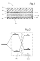
- FIG. 1 schematically shows a semiconductor component 10 according to the invention, which is designed in particular as a solar cell.
- This semiconductor device 10 consists in the present embodiment of a multilayer Structure and it may, for example, along with a number of juxtaposed cells in a paneled form Enclosed metal housing, which is not shown in detail.
- the solar cell preferably has a cover plate with a transparent Material, e.g. a glass layer 11 or the like, thereby this cell against mechanical forces, such as blows, etc., is generally protected against moisture and / or weathering.
- a laminate layer 12, for example of resin, encloses together with a arranged on the bottom, e.g. designed as a ceramic plate Isolator 14 the solar cell, thus completing the interior of the solar cell and thus impermeable to moisture, water or the like is.
- the semiconductor base material 20 consists of pyrite or iron pyrites, which has a chemical composition of FeS 2 .
- the semiconductor base material 20 is connected or doped at least with boron and phosphorus, wherein in the example shown the semiconductor base material consists of the one FeS 2 layer 20.
- This designed as a solid state semiconductor device 10 is set from the monocrystalline semiconductor base material produced from the purest pyrite 20, a layer of phosphorus 21 and a layer of boron 22 together.
- These Layer of phosphorus 21 and this layer of boron 22 are in this case on the corresponding surfaces of the pyrite layer 20 applied that between the semiconductor base material and the phosphorus (P) and the boron, respectively (B) a compound is prepared in the sense of a doping.
- these layers are phosphorus 21 and boron 22 each in a very thin layer Thickness of a few microns by a below explained Process applied.
- Fig.1 is a solar cell with a simple in the context of the invention Structure structure shown. Of course, both the Conductor materials as well as the semiconductor layer in a different configuration and number provided.
- Such a semiconductor device can be used as a solar cell for the most diverse Designs are used, be it for very small cells, eg. for calculators, as well as solar cells for heating homes and for large plants, by means of which in particular the solar energy in electric current is converted.
- Pyrite or iron gravel as naturally occurring rock is the most widespread sulphide on earth, which for example exists in Spain as a hydrothermally created ore area.
- the individual crystals of pyrite are brass or mortar-colored and very hard, whose Mohs hardness is about 6 to 6.5.
- Pyrite has a thermal expansion coefficient at 90 to 300 K of 4.5x10 -6 K -1 and at 300 to 500 K of 8.4x10 -6 K -1.
- the typical basic forms of the crystal habit of pyrite occur as cubes, as cubic form, as pentagondodecahedron or as octahedron. Another advantage of this semiconductor device is that this pyrite has good environmental compatibility.
- this solar cell 10 According to the generally valid rules of quantum mechanics, only those light quanta whose energy is at least equal to the width of the forbidden zone and at most equal to the energy difference between the lower edge of the valence band and the upper edge of the conduction band are effective.
- the amount of charge carriers generated in the semiconductor depends, in addition to the energy and the number per unit area of the incident photons, on the absorption coefficient a of the semiconductor.
- pyrite has a very high absorption coefficient, which is ⁇ ⁇ 1 ⁇ m at the band edge at ⁇ > 10 5 cm -1 . With the formation of the semiconductor device 10 according to the invention, this property of pyrite has been fully exploited.
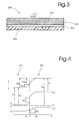
- the energy splitting of the Fe d states in the octahedral O h and the distorted octahedral D 3d ligand field can be seen.
- a band gap of the semiconductor base material is formed by the splitting of the Fe d states into occupied t 2g and unoccupied e g states, this band gap being up to 0.7 eV or more.
- the valence band has a width of 0.8 eV or more and the underlying group is separated by a gap of about 0.8 eV as well.
- the states above the conduction band originate in Fe 4s and 4p states.
- the energy gap in pyrite is generated by splitting the 3d states of the iron into energetically occupied t 2g and unoccupied e g states.
- the splitting is caused by the octahedral ligand field of sulfur, which is slightly distorted and leads to a further, but insignificant splitting of the energy levels.
- FIG. 3 again shows a schematic representation of a cross section of a inventive semiconductor device 50, which consists of at least an upper layer of pyrite 51, which forms the semiconductor base material 40, a layer of boron 52 and a layer of phosphorus 53 joined together is.
- the pyrite 51 is in this case arranged on the top, in which the applied solar radiation or the like is taken as the first become.
- the conductor elements may be arranged such that they cover the layers 51, 52, 53 pick up accordingly, which is not shown in detail.
- the semiconductor base material produced in layers in FIG 40 could be one or more layers of boron and one or more layers of phosphorus across the example as a single crystal be arranged generated pyrite targets.
- the semiconductor base materials 20 and 40 to these solar cells 10, 50 according to the invention can be produced in various ways.
- the pyrite in the composition of FeS 2 can either be obtained from natural occurrence or synthetically produced or grown from iron and sulfur.
- this pyrite which has a net charge carrier concentration of about 10 15 cm -3 , must be repeatedly zone-purified in a manner known per se in order to achieve a defined degree of purity.
- the compounding or doping materials phosphorus and boron are likewise to be provided with the highest degree of purity in order to be able to produce the cells according to the invention of the highest quality from these.
- the production method is, inter alia, the gas phase transport (CVT), in which the temperature gradient when producing the iron-sulfur compound should be between 250 ° and 1200 ° C.
- CVT gas phase transport
- the temperature gradient when producing the iron-sulfur compound should be between 250 ° and 1200 ° C.
- pyrite is used as the natural source material
- the temperature can vary between 250 ° and 850 ° C.
- bromine (Br 2, FeBr 3 ) or another material may be used as a means of transporting sulfur in the iron.
- the crystal growth takes place for example in a sodium polysulfide solution.
- the pyrite can be made from the purified starting iron and sulfur in addition to the standard temperature gradient between 250 ° and 1200 ° C in a gradient of 200 ° to 1400 ° C. These CVT method provides increased reproducibility in the production and it can be used to create absolutely pure crystals.
- the preparation process is preferably via melt solution with tellurium, BrCl 2 . Na, S 2 or similar materials used.
- pyrite is RF sputtering. This is done in a sputtering system, in which a pyrite target with an argon-sulfur plasma sputtered.
- the argon flow is usually between 0.1 and 300 ml / min and the sulfur is removed by evaporation buried by elemental sulfur.
- the used self-bias DC potential is set to 0 to 400 volts.
- the substrate temperature has been chosen from 80 ° to 950 ° C. With this In principle, a poly-crystal structure can also be produced.
- inventive semiconductor devices as Thin films can use an incongruent material system. It Reactive sputtering from a pyrite target, the MOCVD method, is suitable and the spray pyrolysis.
- the thermal evaporation by means of a conveyor system which constantly small amounts of a powder mixture in the hot evaporation source ensures that the material is conditional almost completely evaporated by the high temperature.
- Evaporation results in the advantage that the stoichiometry and a possible doping can be influenced, since, e.g. can add the dopant directly to the powder mixture.
- a Sulfer Deutschen of iron films be it purely thermally or with the help of a Plasmas, it is possible to start from very pure starting materials.
- the thickness of the active layer has a great influence on the efficiency the solar cell. To estimate the efficiency and the For this required cell parameters can be appropriate limits establish.
- the semiconductor base material with phosphorus and boron are preferably used in a mass percentage of 10 -6 to 20% of the base material. This depends on the desired properties of the manufactured semiconductor component.
- the inventive semiconductor device could also be referred to as so-called Tandem cell be made.
- This could, for example, a doped Layer of pyrite and another p and n layer of another Semiconductor crystal, such as of silicon, of gallium or interact from another selectable material.
- a Semiconductor device could be a maximum utilization of the solar spectrum be achieved when using these different semiconductor base materials a coverage of the energy gap between 1.0 and 1.8 eV would take place.
- MBE Molecular Beam Epitaxy
- MOCVD Gas Phase Epitaxy
- the thin-film solar cell with a heterojunction becomes phosphorus and boron, preferably by ion implantation into the surface of the Semiconductor base material pyrite incorporated or doped with the help of Particle accelerators takes place.
- the doping atoms after the Ionization brought to a high energy and shot in the base material, in which they braked to a characteristic depth of penetration be and stay in this.
- the grating of the semiconductor crystal is significantly damaged and it has to be regenerated by a thermal treatment. Diffuse it the implanted impurities and are at the same time built into the grid. Accordingly, mixing profiles of ion implantation and impurity diffusion form.
- the molecular beam epitaxy method is a special vapor deposition process.
- the evaporation material is heated in cylindrical tubes with a small opening at the front evaporated. The size of this opening and the set by heating Vapor pressure in the ovens determine the material transport to the Target.
- Ultra-high vacuum controlled with a mass analyzer as well cooled shielding plates give rise to very clean crystal layers.
- the structure of these crystal layers can be determined by so-called RHEED measurements (Reflected High Energy Electron Diffraction) quasi online controlled and their layer thickness by a temperature control and fast closures are set to an atomic level accurately.
- the semiconductor device can be up to a multilayer structure up to have approximately one hundred layers.
- the semiconductor device according to the Figure 3 of more than three different Layers could be built, so for example several could Layers of pyrite and optionally also several layers Boron or phosphorus may be present.
- the semiconductor device used as pyrite can be - as already above mentioned in the context of the invention not only as single-layer or multi-layer solid-state solar cell, but also as a thin-film solar cell, as MIS solar cell, as a photochemical cell or the like.
- the semiconductor device according to the invention as Solar cell used.
- this semiconductor device could for other purposes such as diode, transistor, Thyristor or the like can be used.
Landscapes
- Photovoltaic Devices (AREA)
- Physical Deposition Of Substances That Are Components Of Semiconductor Devices (AREA)
- Recrystallisation Techniques (AREA)
- Liquid Deposition Of Substances Of Which Semiconductor Devices Are Composed (AREA)
- Chemical Vapour Deposition (AREA)
Abstract
Claims (17)
- Composant semi-conducteur, en particulier cellule solaire, comportant au moins un matériau de base semi-conducteur (20, 40) ayant une structure monocristalline ou polycristalline, lequel matériau est constitué au moins partiellement de pyrite de composition chimique FeS2 et est purifié à un degré de pureté défini, caractérisé en ce que le matériau de base semi-conducteur (20, 40) constitué au moins partiellement de pyrite de composition chimique FeS2 est lié ou dopé au moins avec du bore (52) et du phosphore (53).
- Composant semi-conducteur selon la revendication 1, caractérisé en ce qu'il est prévu dans un matériau de base semi-conducteur multicouche au moins une couche p ou n de pyrite (31) et au moins une couche n ou p d'un autre semi-conducteur (32).
- Composant semi-conducteur selon l'une des revendications précédentes, caractérisé en ce que la concentration en éléments incorporés dans le matériau de base semi-conducteur (20, 40) est comprise entre 10-6 et 20% en poids.
- Composant semi-conducteur selon l'une des revendications précédentes, caractérisé en ce que le composant semi-conducteur est conformé en cellule solaire monocouche ou multicouche, en cellule solaire en couche mince, en cellule solaire MIS ou bien en cellule photochimique.
- Composant semi-conducteur selon l'une des revendications précédentes, caractérisé en ce que la pyrite présente un coefficient de dilatation thermique de 4,5 x 10⁻⁶ K-1 à une température comprise entre 90 et 300 K, et de 8,4 x 10⁻⁶ K-1 à une température comprise entre 300 à 500 K.
- Composant semi-conducteur selon l'une des revendications précédentes, caractérisé en ce que la pyrite de composition chimique FeS2 présente une cellule élémentaire de 12 atomes et d'une longueur d'environ 5,4185 Å (1 Å = 0,1 mm), la forme caractéristique du cristal de pyrite étant celle d'un hexaèdre, d'une cube, d'un dodécaèdre pentagonal ou d'un octaèdre.
- Composant semi-conducteur selon l'une des revendications précédentes, caractérisé en ce que le matériau de base semi-conducteur constitué de pyrite est purifié plusieurs fois par zones.
- Composant semi-conducteur selon l'une des revendications précédentes, caractérisé en ce que la structure multicouche du composant semi-conducteur comporte jusqu'à environ 100 couches.
- Procédé de fabrication d'un composant semi-conducteur, en particulier d'une cellule solaire, selon l'une des revendications précédentes, caractérisé en ce que l'on utilise pour le matériau de base semi-conducteur une pyrite d'origine naturelle ou d'origine synthétique constituée de fer et de soufre de composition chimique FeS2, laquelle pyrite est liée ou dotée avec au moins du bore (52) et du phosphore (53).
- Procédé selon la revendication 10, caractérisé en ce que, dans le cas d'une pyrite de synthèse, la pyrite respectivement les matériaux de départ fer et soufre sont purifiés plusieurs fois par zones à un degré de pureté élevé.
- Procédé selon la revendication 11, caractérisé en ce que la pyrite est fabriquée par un procédé hydrothermal, par un procédé chimique par voie humide.
- Procédé selon la revendication 10, caractérisé en ce que la pyrite est fabriquée par un procédé de fusion de tellure, de NaS2, ou de FeCl2.
- Procédé selon la revendication 10, caractérisé en ce que la pyrite est fabriquée et/ou dopée par les procédés de transfert en phase gazeuse.
- Procédé selon la revendication 14, caractérisé en ce que l'on utilise dans le transfert en phase gazeuse le vecteur Br2.
- Procédé selon la revendication 10, caractérisé en ce que la fabrication de la pyrite est réalisée par une procédé de sulfuration par plasma, de sulfuration par voie thermique, MOCVD, de pulvérisation réactive ou de pyrolyse par pulvérisation.
- Procédé selon la revendication 10, caractérisé en ce que le bore et le phosphore sont liés ou dopés par un procédé d'épitaxie avec le matériau de base pyrite.
- Procédé selon la revendication 10, caractérisé en ce que le bore et le phosphore sont liés ou dopés par un procédé d'implantation ionique avec le matériau de base pyrite.
Priority Applications (2)
| Application Number | Priority Date | Filing Date | Title |
|---|---|---|---|
| DK98948658T DK1032949T3 (da) | 1998-04-29 | 1998-10-23 | Halvlederkomponent, især solcelle, samt fremgangsmåde til fremstilling heraf |
| EP98948658A EP1032949B1 (fr) | 1998-04-29 | 1998-10-23 | Composant a semi-conducteur, notamment pile solaire et procede permettant de l'obtenir |
Applications Claiming Priority (4)
| Application Number | Priority Date | Filing Date | Title |
|---|---|---|---|
| EP98810382A EP0954033A1 (fr) | 1998-04-29 | 1998-04-29 | Dispositif semi-conducteur, en particulier une cellule solaire, ayant une couche de pyrite et méthode de fabrication |
| EP98810382 | 1998-04-29 | ||
| PCT/CH1998/000455 WO1999056325A1 (fr) | 1998-04-29 | 1998-10-23 | Composant a semi-conducteur, notamment pile solaire et procede permettant de l'obtenir |
| EP98948658A EP1032949B1 (fr) | 1998-04-29 | 1998-10-23 | Composant a semi-conducteur, notamment pile solaire et procede permettant de l'obtenir |
Publications (2)
| Publication Number | Publication Date |
|---|---|
| EP1032949A1 EP1032949A1 (fr) | 2000-09-06 |
| EP1032949B1 true EP1032949B1 (fr) | 2005-01-19 |
Family
ID=8236060
Family Applications (2)
| Application Number | Title | Priority Date | Filing Date |
|---|---|---|---|
| EP98810382A Withdrawn EP0954033A1 (fr) | 1998-04-29 | 1998-04-29 | Dispositif semi-conducteur, en particulier une cellule solaire, ayant une couche de pyrite et méthode de fabrication |
| EP98948658A Expired - Lifetime EP1032949B1 (fr) | 1998-04-29 | 1998-10-23 | Composant a semi-conducteur, notamment pile solaire et procede permettant de l'obtenir |
Family Applications Before (1)
| Application Number | Title | Priority Date | Filing Date |
|---|---|---|---|
| EP98810382A Withdrawn EP0954033A1 (fr) | 1998-04-29 | 1998-04-29 | Dispositif semi-conducteur, en particulier une cellule solaire, ayant une couche de pyrite et méthode de fabrication |
Country Status (26)
| Country | Link |
|---|---|
| US (1) | US6635942B2 (fr) |
| EP (2) | EP0954033A1 (fr) |
| JP (1) | JP3874429B2 (fr) |
| KR (1) | KR100613524B1 (fr) |
| CN (1) | CN1218405C (fr) |
| AR (1) | AR019111A1 (fr) |
| AT (1) | ATE287576T1 (fr) |
| AU (1) | AU756671B2 (fr) |
| BG (1) | BG64069B1 (fr) |
| BR (1) | BR9808074B1 (fr) |
| CA (1) | CA2275298C (fr) |
| CZ (1) | CZ298589B6 (fr) |
| DE (1) | DE59812504D1 (fr) |
| DK (1) | DK1032949T3 (fr) |
| ES (1) | ES2239406T3 (fr) |
| HU (1) | HU227655B1 (fr) |
| IL (1) | IL131534A (fr) |
| MY (1) | MY124379A (fr) |
| NO (1) | NO993552L (fr) |
| NZ (1) | NZ336848A (fr) |
| PL (1) | PL192742B1 (fr) |
| PT (1) | PT1032949E (fr) |
| RU (1) | RU2219620C2 (fr) |
| TR (1) | TR199903266T1 (fr) |
| TW (1) | TW434915B (fr) |
| WO (1) | WO1999056325A1 (fr) |
Families Citing this family (13)
| Publication number | Priority date | Publication date | Assignee | Title |
|---|---|---|---|---|
| CN1300375C (zh) * | 2004-12-07 | 2007-02-14 | 浙江大学 | 电沉积氧化及热硫化合成二硫化铁薄膜的方法 |
| JP4938314B2 (ja) * | 2006-01-16 | 2012-05-23 | シャープ株式会社 | 光電変換装置および半導体接合素子の製造方法 |
| US8093684B2 (en) * | 2006-01-16 | 2012-01-10 | Sharp Kabushiki Kaisha | Iron sulfide semiconductor doped with Mg or Zn, junction devices and photoelectric converter comprising same |
| US20110240108A1 (en) | 2010-04-02 | 2011-10-06 | Matt Law | Method To Synthesize Colloidal Iron Pyrite (FeS2) Nanocrystals And Fabricate Iron Pyrite Thin Film Solar Cells |
| US10680125B2 (en) * | 2011-11-15 | 2020-06-09 | Nutech Ventures | Iron pyrite nanocrystals |
| JP5377732B2 (ja) * | 2012-09-14 | 2013-12-25 | シャープ株式会社 | 半導体、p型半導体、半導体接合素子、pn接合素子、および光電変換装置 |
| WO2014209834A2 (fr) * | 2013-06-24 | 2014-12-31 | Arizona Board Of Regents On Behalf Of Arizona State University | Procédé d'obtention de pyrite |
| US9705012B2 (en) * | 2014-03-18 | 2017-07-11 | The United States Of America, As Represented By The Secretary Of The Navy | Method of passivating an iron disulfide surface via encapsulation in zinc sulfide |
| US10181598B2 (en) | 2015-01-05 | 2019-01-15 | University Of Florida Resarch Foundation, Inc. | Lithium ion battery cathodes, methods of making, and methods of use thereof |
| CN105140338B (zh) * | 2015-07-29 | 2017-07-04 | 云南师范大学 | 一种低成本FeS2薄膜太阳电池的制备方法 |
| EP3418717A1 (fr) | 2017-06-23 | 2018-12-26 | Cellix Limited | Dispositif microfluidique pour séparer des particules |
| EP3418719A1 (fr) | 2017-06-23 | 2018-12-26 | Cellix Limited | Système et procédé pour le identification améliorée de particules ou de cellules |
| EP3418721A1 (fr) | 2017-06-23 | 2018-12-26 | Cellix Limited | Puce microfluide |
Family Cites Families (10)
| Publication number | Priority date | Publication date | Assignee | Title |
|---|---|---|---|---|
| US3852563A (en) * | 1974-02-01 | 1974-12-03 | Hewlett Packard Co | Thermal printing head |
| US4131486A (en) * | 1977-01-19 | 1978-12-26 | The United States Of America As Represented By The Administrator Of The National Aeronautics And Space Administration | Back wall solar cell |
| US4710786A (en) * | 1978-03-16 | 1987-12-01 | Ovshinsky Stanford R | Wide band gap semiconductor alloy material |
| JPS59115574A (ja) * | 1982-12-23 | 1984-07-04 | Semiconductor Energy Lab Co Ltd | 光電変換装置作製方法 |
| US4589918A (en) * | 1984-03-28 | 1986-05-20 | National Research Institute For Metals | Thermal shock resistant thermoelectric material |
| DE3526910A1 (de) * | 1984-07-27 | 1986-02-13 | Hahn-Meitner-Institut für Kernforschung Berlin GmbH, 1000 Berlin | Photoaktive pyritschicht, verfahren zu deren herstellung und verwendung derartiger pyritschichten |
| CA1265922A (fr) * | 1984-07-27 | 1990-02-20 | Helmut Tributsch | Couche photo-active de pyrite, sa preparation et son emploi |
| US4766471A (en) * | 1986-01-23 | 1988-08-23 | Energy Conversion Devices, Inc. | Thin film electro-optical devices |
| FR2694451B1 (fr) * | 1992-07-29 | 1994-09-30 | Asulab Sa | Cellule photovoltaïque. |
| CA2110097C (fr) * | 1992-11-30 | 2002-07-09 | Soichiro Kawakami | Batterie secondaire |
-
1998
- 1998-04-29 EP EP98810382A patent/EP0954033A1/fr not_active Withdrawn
- 1998-10-23 IL IL13153498A patent/IL131534A/en not_active IP Right Cessation
- 1998-10-23 RU RU99118904/28A patent/RU2219620C2/ru not_active IP Right Cessation
- 1998-10-23 HU HU0004391A patent/HU227655B1/hu not_active IP Right Cessation
- 1998-10-23 PT PT98948658T patent/PT1032949E/pt unknown
- 1998-10-23 AT AT98948658T patent/ATE287576T1/de active
- 1998-10-23 CA CA002275298A patent/CA2275298C/fr not_active Expired - Fee Related
- 1998-10-23 PL PL337092A patent/PL192742B1/pl unknown
- 1998-10-23 US US09/319,772 patent/US6635942B2/en not_active Expired - Lifetime
- 1998-10-23 CN CN988024780A patent/CN1218405C/zh not_active Expired - Fee Related
- 1998-10-23 JP JP54086599A patent/JP3874429B2/ja not_active Expired - Fee Related
- 1998-10-23 WO PCT/CH1998/000455 patent/WO1999056325A1/fr not_active Ceased
- 1998-10-23 AU AU95275/98A patent/AU756671B2/en not_active Ceased
- 1998-10-23 BR BRPI9808074-1A patent/BR9808074B1/pt not_active IP Right Cessation
- 1998-10-23 EP EP98948658A patent/EP1032949B1/fr not_active Expired - Lifetime
- 1998-10-23 TR TR1999/03266T patent/TR199903266T1/xx unknown
- 1998-10-23 NZ NZ336848A patent/NZ336848A/en not_active IP Right Cessation
- 1998-10-23 ES ES98948658T patent/ES2239406T3/es not_active Expired - Lifetime
- 1998-10-23 DK DK98948658T patent/DK1032949T3/da active
- 1998-10-23 DE DE59812504T patent/DE59812504D1/de not_active Expired - Lifetime
- 1998-10-23 CZ CZ0150499A patent/CZ298589B6/cs not_active IP Right Cessation
- 1998-10-23 KR KR1019997006817A patent/KR100613524B1/ko not_active Expired - Fee Related
-
1999
- 1999-04-26 MY MYPI99001623A patent/MY124379A/en unknown
- 1999-04-27 AR ARP990101934A patent/AR019111A1/es active IP Right Grant
- 1999-04-28 TW TW088106833A patent/TW434915B/zh not_active IP Right Cessation
- 1999-07-20 NO NO993552A patent/NO993552L/no not_active Application Discontinuation
- 1999-09-01 BG BG103706A patent/BG64069B1/bg unknown
Also Published As
Similar Documents
| Publication | Publication Date | Title |
|---|---|---|
| EP1032949B1 (fr) | Composant a semi-conducteur, notamment pile solaire et procede permettant de l'obtenir | |
| DE112011103244T5 (de) | Mehrfachübergangssolarzelle mit schwachnitridischer Teilzelle, die eine graduierte Dotierung aufweist | |
| WO2009141132A2 (fr) | Système multicouche pour cellules solaires | |
| DE2844070A1 (de) | Amorpher halbleiter | |
| EP2438634A1 (fr) | Matériau composite comprenant des nanoparticules ainsi que production de couches photoactives contenant des nanoparticules semi-conductrices quaternaires, pentanaires et supérieures | |
| DE2304552A1 (de) | Anordnung zur erzeugung elektromagnetischer wellen | |
| DE102014210753B4 (de) | Halbleiterbauelement auf Basis von In(AlGa)As und dessen Verwendung | |
| EP0173642A2 (fr) | Couche de pyrite photoactive, méthode pour sa préparation et application de telles couches de pyrite | |
| Chandramohan et al. | Implantation-assisted Co-doped CdS thin films: Structural, optical, and vibrational properties | |
| DE2449542C3 (de) | Verfahren zur Herstellung einer amorphen Schicht auf einem Halbleitersubstrat | |
| EP1972014A1 (fr) | Matériau semi-conducteur actif photovoltaïque et cellule photovoltaïque | |
| DE2734203A1 (de) | Hetero-uebergangslaser | |
| CH663609A5 (de) | Stabile, phosphor enthaltende feststoff-ablagerungen, verfahren zu deren herstellung sowie verwendungen der genannten ablagerungen. | |
| DE102013101247A1 (de) | Vorrichtung und Verfahren zum Herstellen von Solarzellen | |
| DE2848925A1 (de) | Lawinen-photodiode mit heterouebergang | |
| EP2865011B1 (fr) | Système de couche pour cellules solaires à couche mince avec couche-tampon en naxin1syclz | |
| DE102015109786A1 (de) | Verfahren zur Herstellung eines optoelektronischen Halbleiterbauelements sowie optoelektronisches Halbleiterbauelement | |
| DE10108700A1 (de) | Optisches Material und optisches Element | |
| DE69303738T2 (de) | Photoelektrischer Detektor mit Quantentöpfen und verbesserter Detectivität | |
| DE2813671A1 (de) | Photovoltaisches halbleiterelement zur ermittlung elektromagnetischer strahlungen | |
| EP0681336A2 (fr) | Dispositif électronique avec une structure composite à semi-conducteur | |
| DE112022001998T5 (de) | Eine Tandem-Solarzelle mit selektiver spektraler Absorption und Durchlässigkeit und deren Verfahren | |
| Sunamura et al. | Photoluminescence investigation on growth mode changeover in Ge-rich Si1− xGex/Si strained quantum wells | |
| EP2469608A1 (fr) | Diode bipolaire dotée d'un absorbeur de structure quantique optique | |
| WO1995015011A1 (fr) | Dispositif photovoltaique |
Legal Events
| Date | Code | Title | Description |
|---|---|---|---|
| PUAI | Public reference made under article 153(3) epc to a published international application that has entered the european phase |
Free format text: ORIGINAL CODE: 0009012 |
|
| 17P | Request for examination filed |
Effective date: 20000619 |
|
| AK | Designated contracting states |
Kind code of ref document: A1 Designated state(s): AT BE CH DE DK ES FI FR GB GR IE IT LI LU MC NL PT SE |
|
| 17Q | First examination report despatched |
Effective date: 20010504 |
|
| GRAP | Despatch of communication of intention to grant a patent |
Free format text: ORIGINAL CODE: EPIDOSNIGR1 |
|
| GRAS | Grant fee paid |
Free format text: ORIGINAL CODE: EPIDOSNIGR3 |
|
| GRAA | (expected) grant |
Free format text: ORIGINAL CODE: 0009210 |
|
| AK | Designated contracting states |
Kind code of ref document: B1 Designated state(s): AT BE CH DE DK ES FI FR GB GR IE IT LI LU MC NL PT SE |
|
| REG | Reference to a national code |
Ref country code: GB Ref legal event code: FG4D Free format text: NOT ENGLISH |
|
| REG | Reference to a national code |
Ref country code: CH Ref legal event code: EP |
|
| REG | Reference to a national code |
Ref country code: IE Ref legal event code: FG4D Free format text: GERMAN |
|
| REF | Corresponds to: |
Ref document number: 59812504 Country of ref document: DE Date of ref document: 20050224 Kind code of ref document: P |
|
| REG | Reference to a national code |
Ref country code: CH Ref legal event code: NV Representative=s name: LUCHS & PARTNER PATENTANWAELTE |
|
| REG | Reference to a national code |
Ref country code: SE Ref legal event code: TRGR |
|
| GBT | Gb: translation of ep patent filed (gb section 77(6)(a)/1977) |
Effective date: 20050418 |
|
| REG | Reference to a national code |
Ref country code: GR Ref legal event code: EP Ref document number: 20050401302 Country of ref document: GR |
|
| REG | Reference to a national code |
Ref country code: DK Ref legal event code: T3 |
|
| REG | Reference to a national code |
Ref country code: PT Ref legal event code: SC4A Free format text: AVAILABILITY OF NATIONAL TRANSLATION Effective date: 20050415 |
|
| REG | Reference to a national code |
Ref country code: ES Ref legal event code: FG2A Ref document number: 2239406 Country of ref document: ES Kind code of ref document: T3 |
|
| APAH | Appeal reference modified |
Free format text: ORIGINAL CODE: EPIDOSCREFNO |
|
| PLBE | No opposition filed within time limit |
Free format text: ORIGINAL CODE: 0009261 |
|
| STAA | Information on the status of an ep patent application or granted ep patent |
Free format text: STATUS: NO OPPOSITION FILED WITHIN TIME LIMIT |
|
| ET | Fr: translation filed | ||
| 26N | No opposition filed |
Effective date: 20051020 |
|
| REG | Reference to a national code |
Ref country code: FR Ref legal event code: PLFP Year of fee payment: 18 |
|
| PGFP | Annual fee paid to national office [announced via postgrant information from national office to epo] |
Ref country code: LU Payment date: 20151023 Year of fee payment: 18 |
|
| PGFP | Annual fee paid to national office [announced via postgrant information from national office to epo] |
Ref country code: DK Payment date: 20151021 Year of fee payment: 18 |
|
| PGFP | Annual fee paid to national office [announced via postgrant information from national office to epo] |
Ref country code: GB Payment date: 20151013 Year of fee payment: 18 Ref country code: IT Payment date: 20151028 Year of fee payment: 18 Ref country code: IE Payment date: 20151028 Year of fee payment: 18 Ref country code: DE Payment date: 20151030 Year of fee payment: 18 Ref country code: FI Payment date: 20151022 Year of fee payment: 18 Ref country code: GR Payment date: 20151030 Year of fee payment: 18 |
|
| PGFP | Annual fee paid to national office [announced via postgrant information from national office to epo] |
Ref country code: BE Payment date: 20151019 Year of fee payment: 18 Ref country code: AT Payment date: 20151028 Year of fee payment: 18 Ref country code: SE Payment date: 20151021 Year of fee payment: 18 Ref country code: NL Payment date: 20151021 Year of fee payment: 18 Ref country code: MC Payment date: 20151023 Year of fee payment: 18 Ref country code: ES Payment date: 20151022 Year of fee payment: 18 Ref country code: FR Payment date: 20151023 Year of fee payment: 18 Ref country code: PT Payment date: 20151019 Year of fee payment: 18 |
|
| PG25 | Lapsed in a contracting state [announced via postgrant information from national office to epo] |
Ref country code: BE Free format text: LAPSE BECAUSE OF NON-PAYMENT OF DUE FEES Effective date: 20161031 |
|
| REG | Reference to a national code |
Ref country code: DE Ref legal event code: R119 Ref document number: 59812504 Country of ref document: DE |
|
| REG | Reference to a national code |
Ref country code: DK Ref legal event code: EBP Effective date: 20161031 |
|
| REG | Reference to a national code |
Ref country code: NL Ref legal event code: MM Effective date: 20161101 |
|
| REG | Reference to a national code |
Ref country code: AT Ref legal event code: MM01 Ref document number: 287576 Country of ref document: AT Kind code of ref document: T Effective date: 20161023 |
|
| GBPC | Gb: european patent ceased through non-payment of renewal fee |
Effective date: 20161023 |
|
| PG25 | Lapsed in a contracting state [announced via postgrant information from national office to epo] |
Ref country code: MC Free format text: LAPSE BECAUSE OF NON-PAYMENT OF DUE FEES Effective date: 20161031 |
|
| REG | Reference to a national code |
Ref country code: IE Ref legal event code: MM4A |
|
| REG | Reference to a national code |
Ref country code: FR Ref legal event code: ST Effective date: 20170630 |
|
| PG25 | Lapsed in a contracting state [announced via postgrant information from national office to epo] |
Ref country code: GB Free format text: LAPSE BECAUSE OF NON-PAYMENT OF DUE FEES Effective date: 20161023 Ref country code: FR Free format text: LAPSE BECAUSE OF NON-PAYMENT OF DUE FEES Effective date: 20161102 Ref country code: GR Free format text: LAPSE BECAUSE OF NON-PAYMENT OF DUE FEES Effective date: 20170504 Ref country code: FI Free format text: LAPSE BECAUSE OF NON-PAYMENT OF DUE FEES Effective date: 20161023 Ref country code: DE Free format text: LAPSE BECAUSE OF NON-PAYMENT OF DUE FEES Effective date: 20170503 |
|
| PG25 | Lapsed in a contracting state [announced via postgrant information from national office to epo] |
Ref country code: SE Free format text: LAPSE BECAUSE OF NON-PAYMENT OF DUE FEES Effective date: 20161024 Ref country code: AT Free format text: LAPSE BECAUSE OF NON-PAYMENT OF DUE FEES Effective date: 20161023 Ref country code: LU Free format text: LAPSE BECAUSE OF NON-PAYMENT OF DUE FEES Effective date: 20161023 Ref country code: NL Free format text: LAPSE BECAUSE OF NON-PAYMENT OF DUE FEES Effective date: 20161101 Ref country code: PT Free format text: LAPSE BECAUSE OF NON-PAYMENT OF DUE FEES Effective date: 20170424 |
|
| PG25 | Lapsed in a contracting state [announced via postgrant information from national office to epo] |
Ref country code: IT Free format text: LAPSE BECAUSE OF NON-PAYMENT OF DUE FEES Effective date: 20161023 |
|
| PGFP | Annual fee paid to national office [announced via postgrant information from national office to epo] |
Ref country code: CH Payment date: 20170928 Year of fee payment: 20 |
|
| PG25 | Lapsed in a contracting state [announced via postgrant information from national office to epo] |
Ref country code: DK Free format text: LAPSE BECAUSE OF NON-PAYMENT OF DUE FEES Effective date: 20161031 Ref country code: IE Free format text: LAPSE BECAUSE OF NON-PAYMENT OF DUE FEES Effective date: 20161023 |
|
| REG | Reference to a national code |
Ref country code: BE Ref legal event code: MM Effective date: 20161031 |
|
| REG | Reference to a national code |
Ref country code: ES Ref legal event code: FD2A Effective date: 20180507 |
|
| PG25 | Lapsed in a contracting state [announced via postgrant information from national office to epo] |
Ref country code: ES Free format text: LAPSE BECAUSE OF FAILURE TO SUBMIT A TRANSLATION OF THE DESCRIPTION OR TO PAY THE FEE WITHIN THE PRESCRIBED TIME-LIMIT Effective date: 20050119 |
|
| PG25 | Lapsed in a contracting state [announced via postgrant information from national office to epo] |
Ref country code: ES Free format text: LAPSE BECAUSE OF FAILURE TO SUBMIT A TRANSLATION OF THE DESCRIPTION OR TO PAY THE FEE WITHIN THE PRESCRIBED TIME-LIMIT Effective date: 20161024 |
|
| REG | Reference to a national code |
Ref country code: CH Ref legal event code: PL |