EP1033675A2 - Kontaktlose Informationsspeicherungsvorrichtung - Google Patents
Kontaktlose Informationsspeicherungsvorrichtung Download PDFInfo
- Publication number
- EP1033675A2 EP1033675A2 EP00104426A EP00104426A EP1033675A2 EP 1033675 A2 EP1033675 A2 EP 1033675A2 EP 00104426 A EP00104426 A EP 00104426A EP 00104426 A EP00104426 A EP 00104426A EP 1033675 A2 EP1033675 A2 EP 1033675A2
- Authority
- EP
- European Patent Office
- Prior art keywords
- information storage
- storage device
- molded case
- wireless
- coil antenna
- Prior art date
- Legal status (The legal status is an assumption and is not a legal conclusion. Google has not performed a legal analysis and makes no representation as to the accuracy of the status listed.)
- Withdrawn
Links
Images




Classifications
-
- G—PHYSICS
- G06—COMPUTING OR CALCULATING; COUNTING
- G06K—GRAPHICAL DATA READING; PRESENTATION OF DATA; RECORD CARRIERS; HANDLING RECORD CARRIERS
- G06K19/00—Record carriers for use with machines and with at least a part designed to carry digital markings
- G06K19/06—Record carriers for use with machines and with at least a part designed to carry digital markings characterised by the kind of the digital marking, e.g. shape, nature, code
- G06K19/067—Record carriers with conductive marks, printed circuits or semiconductor circuit elements, e.g. credit or identity cards also with resonating or responding marks without active components
- G06K19/07—Record carriers with conductive marks, printed circuits or semiconductor circuit elements, e.g. credit or identity cards also with resonating or responding marks without active components with integrated circuit chips
- G06K19/077—Constructional details, e.g. mounting of circuits in the carrier
- G06K19/07749—Constructional details, e.g. mounting of circuits in the carrier the record carrier being capable of non-contact communication, e.g. constructional details of the antenna of a non-contact smart card
- G06K19/07773—Antenna details
- G06K19/07777—Antenna details the antenna being of the inductive type
- G06K19/07779—Antenna details the antenna being of the inductive type the inductive antenna being a coil
-
- G—PHYSICS
- G06—COMPUTING OR CALCULATING; COUNTING
- G06K—GRAPHICAL DATA READING; PRESENTATION OF DATA; RECORD CARRIERS; HANDLING RECORD CARRIERS
- G06K19/00—Record carriers for use with machines and with at least a part designed to carry digital markings
- G06K19/06—Record carriers for use with machines and with at least a part designed to carry digital markings characterised by the kind of the digital marking, e.g. shape, nature, code
- G06K19/067—Record carriers with conductive marks, printed circuits or semiconductor circuit elements, e.g. credit or identity cards also with resonating or responding marks without active components
- G06K19/07—Record carriers with conductive marks, printed circuits or semiconductor circuit elements, e.g. credit or identity cards also with resonating or responding marks without active components with integrated circuit chips
- G06K19/077—Constructional details, e.g. mounting of circuits in the carrier
- G06K19/07749—Constructional details, e.g. mounting of circuits in the carrier the record carrier being capable of non-contact communication, e.g. constructional details of the antenna of a non-contact smart card
-
- G—PHYSICS
- G06—COMPUTING OR CALCULATING; COUNTING
- G06K—GRAPHICAL DATA READING; PRESENTATION OF DATA; RECORD CARRIERS; HANDLING RECORD CARRIERS
- G06K19/00—Record carriers for use with machines and with at least a part designed to carry digital markings
- G06K19/06—Record carriers for use with machines and with at least a part designed to carry digital markings characterised by the kind of the digital marking, e.g. shape, nature, code
- G06K19/067—Record carriers with conductive marks, printed circuits or semiconductor circuit elements, e.g. credit or identity cards also with resonating or responding marks without active components
- G06K19/07—Record carriers with conductive marks, printed circuits or semiconductor circuit elements, e.g. credit or identity cards also with resonating or responding marks without active components with integrated circuit chips
- G06K19/077—Constructional details, e.g. mounting of circuits in the carrier
- G06K19/07749—Constructional details, e.g. mounting of circuits in the carrier the record carrier being capable of non-contact communication, e.g. constructional details of the antenna of a non-contact smart card
- G06K19/07796—Constructional details, e.g. mounting of circuits in the carrier the record carrier being capable of non-contact communication, e.g. constructional details of the antenna of a non-contact smart card arrangements on the record carrier to allow stacking of a plurality of similar record carriers, e.g. to avoid interference between the non-contact communication of the plurality of record carriers
-
- G—PHYSICS
- G06—COMPUTING OR CALCULATING; COUNTING
- G06K—GRAPHICAL DATA READING; PRESENTATION OF DATA; RECORD CARRIERS; HANDLING RECORD CARRIERS
- G06K7/00—Methods or arrangements for sensing record carriers, e.g. for reading patterns
- G06K7/0008—General problems related to the reading of electronic memory record carriers, independent of its reading method, e.g. power transfer
-
- G—PHYSICS
- G06—COMPUTING OR CALCULATING; COUNTING
- G06K—GRAPHICAL DATA READING; PRESENTATION OF DATA; RECORD CARRIERS; HANDLING RECORD CARRIERS
- G06K7/00—Methods or arrangements for sensing record carriers, e.g. for reading patterns
- G06K7/10—Methods or arrangements for sensing record carriers, e.g. for reading patterns by electromagnetic radiation, e.g. optical sensing; by corpuscular radiation
- G06K7/10009—Methods or arrangements for sensing record carriers, e.g. for reading patterns by electromagnetic radiation, e.g. optical sensing; by corpuscular radiation sensing by radiation using wavelengths larger than 0.1 mm, e.g. radio-waves or microwaves
- G06K7/10316—Methods or arrangements for sensing record carriers, e.g. for reading patterns by electromagnetic radiation, e.g. optical sensing; by corpuscular radiation sensing by radiation using wavelengths larger than 0.1 mm, e.g. radio-waves or microwaves using at least one antenna particularly designed for interrogating the wireless record carriers
- G06K7/10336—Methods or arrangements for sensing record carriers, e.g. for reading patterns by electromagnetic radiation, e.g. optical sensing; by corpuscular radiation sensing by radiation using wavelengths larger than 0.1 mm, e.g. radio-waves or microwaves using at least one antenna particularly designed for interrogating the wireless record carriers the antenna being of the near field type, inductive coil
Definitions
- the present invention generally relates to a wireless information storage device and a method for putting a wireless information storage device on or into an article. More particularly, the present invention relates to a device and a method for achieving both certainty and efficiency of a plurality of wireless information storage devices being communicated by a reader/writer system at a time,
- a wireless information storage device such as a wireless card or a wireless tag, has recently attracted a great deal of attention as an internal information carrier of the next generation because of its capability to read and write information with an external reader/writer system while being not being connected to the external system.
- the wireless information storage device comprises a loop-shaped coil antenna that transmits signals to and receives signals from a wireless transmitter/receiver via wireless communication.
- the wireless transmitter/receiver comprises a large scale integrated circuit (LSI) and a memory for storing information.
- the wireless transmitter/receiver generates information, such as read, write, or command data, by demodulating a signal received via a coil antenna.
- the wireless transmitter/receiver also generates a signal to be transmitted via the coil antenna by modulating information.
- Both the antenna and the wireless transmitter/receiver may be molded in a plastic case hereinafter referred to as "molded case.”
- a multi-reader/writer system is used to communicate with the wireless information storage device.
- the multi-reader/writer system communicates with a plurality of wireless storage devices using single antenna.
- the multi-reader/writer system requires that the wireless information storage devices are not perfectly stacked, arid thus not aligned so that the system could process information unerringly.
- a 'coupling coil' that is composed of all the aligned coil antennas is created.
- the coupling coil causes a shift of the resonance point of each wireless information storage device. Furthermore, as the number of wireless information storage devices perfectly stacked increases, an electromotive force generated in the coil antenna of each of the wireless information storage devices is weakened because a magnetic flux going through the coil antenna is weakened.
- the multi-reader/writer system can not process information unerringly. Therefore, the efficiency for processing information for each wireless information storage device is low.
- each of a plurality of wireless information storage devices is located at the same position of an item, such as a compact disc (CD), to be communicated at a time, the efficiency for processing information for each item is low by the same reason.
- an item such as a compact disc (CD)
- the present invention solves the inherent limitations of existing wireless information storage device and a method for putting a wireless information storage device on or into an item that substantially obviates one or more of the problems due to limitations and disadvantages of the past approaches.
- the present invention is directed to a wireless information storage device.
- the device comprises a coil antenna, a memory, a control unit, and a molded case.
- the coil antenna having a two-dimensional center for transmits and/or receives a signal via wireless communication.
- the memory stares information.
- the control unit that generates information by demodulating a signal received via the coil antenna, and generates a signal to be transmitted via the coil antenna by modulating information stored in the memory.
- the mold ease includes the coil antenna.
- the two-dimensional center of the coil antenna is off from the two-dimensional center of the molded case.
- a wireless information storage device comprising a coil antenna, a memory, a control, and a molded case.
- the coil antenna has a two-dimensional center for transmitting and/or receiving a signal via wireless communication transmitting and/or receiving a signal via wireless communication.
- the memory stores information.
- the control unit generates information by demodulating a signal received via the coil antenna, and generates a signal to be transmitted via the coil antenna by modulating information stored in the memory.
- the mold case having a two-dimensional center includes the coil antenna. Each coil antenna is located at a position in the device relatively different from each other when a plurality of devices is perfectly stacked.
- an item has a two-dimensional center, and contains a wireless information storage device.
- the wireless information storage device also has a two-dimensional center.
- the item comprises a coil antenna, a memory, a control unit, and a molded case.
- the coil antenna transmits and/or receives a signal via wireless communication.
- the memory stores information.
- the control unit generates information by demodulating a signal received via the coil antenna, and generates a signal to be transmitted via the coil antenna by modulating information stored in the memory.
- the molded case includes the coil antenna.
- the two-dimensional center of the wireless information storage device is off from the two-dimensional center of the item.
- a method for putting a wireless information storage device containing a coil antenna and a board-shaped molded case on or into a board-shaped item having a two-dimensional center comprises the step of putting the wireless information storage device on or into the two-dimensional center of the item.
- FIG. 1(a) is an exemplary horizontal cross section of a wireless information storage device 100 according to a first embodiment of the present invention.
- FIG. 1(b) is an exemplary vertical cross section of wireless information storage device 100 sectioned at a line A-A shown in FIG. 1(a).
- Wireless information storage device 100 such as a wireless tag is included in or attached to an item (not shown).
- An external reader/writer system (further described below) reads information regarding the item from wireless information storage device 100 and writes information to wireless information storage device 100 as needed using a wireless communication.
- Wireless information storage device 100 comprises an antenna 102, a wireless transmitter/receiver 104, and a molded ease 106.
- Antenna 102 which has a loop-shaped coil, transmits signals to wireless transmitter/receiver 104 and also receives signals from wireless transmitter/receiver 104.
- Wireless transmitter/receiver 104 which comprises a large scale integrated circuit (LSI). generates information by demodulating a received signal.
- Wireless transmitter/receiver 104 also generates a signal to be transmitted by modulating information stored in a memory (further described below). Molded case 106 includes antenna 102 and wireless transmitter/receiver 104.
- LSI large scale integrated circuit
- Molded case 106 may be a round-and-board-shaped disk. Molded case 106 may be 20mm in diameter and 3-5mm thick.
- loop-shaped coil antenna 102 is located with its center C1 off centered from the center C2 (i.e., gravitational center) of round-shaped molded case 106.
- loop-shaped coil antenna 102 is located with its central axis L1 being approximately parallel to an axis perpendicular to the piano surface of molded case 106 and also off centered from central axis L2 of molded case 106.
- wireless information storage device 100 is produced with antenna 102, which is included in or attached to wireless information storage device 100, purposely off centered from the center of the molded case 106.
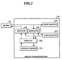
- FIG. 2 is an exemplary block diagram depicting the configuration of wireless transmitter/receiver 104.
- Wireless transmitter/receiver 104 comprises a power generator 200, a clock generator 202, a demodulator 204, a modulator 206, a controller 208, and a nonvolatile memory 210.
- Power generator 200 generates electric power to be provided to each internal part of the device 100 by both rectifying and ballasting a signal received via antenna 102.
- Clock generator 202 generates a clock pulse from a received signal and supplies the clock pulse to each internal part.
- Demodulator 204 generates information to be stored in nonvolatile memory 210 by demodulating a received signal.
- Modulator 206 generates a signal to be transmitted by modulating information stored in nonvolatile memory 210.
- Controller 208 controls reading and writing information with nonvolatile memory 210.
- Nonvolatile memory 210 stores information used for controlling wireless transmitter/receiver 104, information regarding wireless information storage device 100, such as an ID, and information regarding the location of an item.
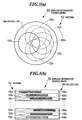
- FIG. 3(a) is an exemplary diagram depicting locations of a plurality of antennas 102 of stacked up wireless information storage devices 100, viewed from the direction perpendicular to the plane surface of molded case 106.
- FIG. 3(b) is an exemplary diagram depicting locations of a plurality of antennas 102 of stacked wireless information storage devices 100, viewed from the direction parallel to the plane surface of molded case 106.
- each antenna 102 is not located at the center of molded cases 106, e.g., 106a, 106b, 106c, ,.., and 106z, as shown in FIG. 3(a).
- the center axis of one of antennas 102 being located at the same position as the center axis of another antenna 102 is located.
- FIG. 4 is an exemplary block diagram depicting the configuration of reader/writer system 400.
- Reader/writer system 400 reads information from the above-described wireless information storage device 102 and also writes information into the above-described wireless information storage device 102 as needed, using a wireless communications.
- Reader/writer system 400 comprises an antenna box 402, a computer 404, and a cable 406 to connect antenna box 402 and computer 404.
- Reader/writer system 400 communicates with perfectly “M” stacked wireless information storage devices 102 in a line and "N” bunches of the devices 102 in a line.
- wireless information storage device 102 When wireless information storage device 102 enters into an area where reader/writer system 400 can communicate, computer 404 instructs antenna box 402 to output a radio wave signal.
- antenna 102 receives the radio wave signal, transforms the radio wave signal into electric signal, and provides the electric signal to both power generator 200 and clock generator 202.
- Power generator 200 generates electric power necessary to drive each internal part using the electric signal and supplies the electric power to each internal part.
- Clock generator 202 generates a clock pulse from the electric signal and supplies the clock to each internal part.
- Antenna 102 also provides the electric signal to demodulator 204.
- Demodulator 204 generates information by demodulating the electric signal.
- Controller 208 then stores the generated information into nonvolatile memory 210.
- controller 208 When controller 208 receives a signal used for a reading information from modulator 204, controller 208 determines the necessity of transmitting information. Controller 208 reads the information from nonvolatile memory 210 and outputs the information to modulator 206. Modulator 206 modulates the information into a signal and transmits the Signal to reader/writer system 400 via antenna 102.
- Reader/writer system 400 receives the transmitted signal via antenna box 402 and computer 404 processes the information read from nonvolatile memory 210.
- wireless information storage device 100 comprising a molded case having other shape will be hereinafter described.
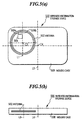
- FIG. 5(a) is an exemplary horizontal cross section of a wireless information storage device 100 according to a second embodiment of the present invention.
- FIG. 5(b) is an exemplary vertical cross section of wireless information storage device 100 sectioned at a line B-B shown in FIG. 5(a).
- Wireless information storage device 500 comprises a loop-shaped antenna 502, a wireless transmitter/receiver 504, and a rectangle-shaped molded case 506.
- Antenna 502 and wireless transmitter/receiver 504 are connected to each other via conductors 508a and 508b.
- loop-shaped coil antenna 502 is located with its center C3 off centered from the center C4 (i.e., gravitational center) of round-shaped molded case 506.
- loop-shaped coil antenna 502 is located with its central axis L3 being approximately parallel to an axis perpendicular to the plane surface of molded case 506 and also off centered from central axis L4 of molded case 506.
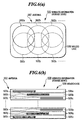
- FIG. 6(a) is an exemplary diagram depicting locations of a plurality of antennas 502 of stacked wireless information storage devices 500, viewed from the direction perpendicular to the plane surface of molded case 506.
- FIG. 6(b) is an exemplary diagram depicting locations of a plurality of antennas 502 of piled up wireless information storage devices 500, viewed from the direction parallel to the plane surface of molded case 506.
- each antenna 502 is not located at the center of molded case 506, e.g., 506a, 506b, 506c, ..., and 506z, as shown in FIG. 6(a).
- the center axis of one of antennas 502 being located at the same position as when the center axis of other antenna 502 is located.
- the item is composed of a nonmetallic material or metallic material which does not influence wireless communication.
- FIG. 7 is an exemplary horizontal cross section of wireless information storage device 700 included in or attached with an article, according to a third embodiment of the present invention.
- Wireless information storage device 700 comprises a loop-shaped antenna 702, a wireless transmitter/receiver 704, and a rectangle-shaped mold case 706. Antenna 702 and wireless transmitter/receiver 704 are connected to each other via conductors 708a and 708b.
- FIG. 8(a) is an exemplary diagram depicting locations of a plurality of wireless information storage device 700 of stacked items 800, viewed from the direction perpendicular to the plane surface of item 800.
- FIG. 6(b) is an exemplary diagram depicting locations of a plurality of wireless information storage device 700 of piled up items 800, viewed from the direction parallel to the plane surface of item 800.
- wireless information storage device 700 e.g., 700a, 700b, 700c, ..., and 700z
- a plurality of item 800 e.g., 800a, 800b, 800c, ..., and 800z
- FIG. 8(b) there is little possibility of these wireless information storage device 700 being located at the same position because each wireless information storage device 700 is not located at the center of item 800 as shown in FIG. 8(a).
- the center axis of one of antennas 702 being located at the same position as the center axis of other antenna 702 is located.
Landscapes
- Engineering & Computer Science (AREA)
- Physics & Mathematics (AREA)
- General Physics & Mathematics (AREA)
- Theoretical Computer Science (AREA)
- Microelectronics & Electronic Packaging (AREA)
- Computer Hardware Design (AREA)
- Toxicology (AREA)
- Artificial Intelligence (AREA)
- Computer Vision & Pattern Recognition (AREA)
- Health & Medical Sciences (AREA)
- Computer Networks & Wireless Communication (AREA)
- General Health & Medical Sciences (AREA)
- Electromagnetism (AREA)
- Near-Field Transmission Systems (AREA)
- Mobile Radio Communication Systems (AREA)
Applications Claiming Priority (2)
| Application Number | Priority Date | Filing Date | Title |
|---|---|---|---|
| JP5571099 | 1999-03-03 | ||
| JP11055710A JP2000251038A (ja) | 1999-03-03 | 1999-03-03 | 無線情報記憶媒体及び無線情報記憶媒体の配置方法 |
Publications (2)
| Publication Number | Publication Date |
|---|---|
| EP1033675A2 true EP1033675A2 (de) | 2000-09-06 |
| EP1033675A3 EP1033675A3 (de) | 2001-09-26 |
Family
ID=13006448
Family Applications (1)
| Application Number | Title | Priority Date | Filing Date |
|---|---|---|---|
| EP00104426A Withdrawn EP1033675A3 (de) | 1999-03-03 | 2000-03-03 | Kontaktlose Informationsspeicherungsvorrichtung |
Country Status (3)
| Country | Link |
|---|---|
| US (1) | US6842606B1 (de) |
| EP (1) | EP1033675A3 (de) |
| JP (1) | JP2000251038A (de) |
Cited By (10)
| Publication number | Priority date | Publication date | Assignee | Title |
|---|---|---|---|---|
| DE10153169A1 (de) * | 2001-10-27 | 2003-05-08 | Wolfgang Habe | Signalspeicherkörper und dessen Verwendung |
| WO2002099730A3 (en) * | 2001-06-05 | 2003-10-02 | 3 M Innovative Properties Comp | Radio frequency identification in document management |
| EP1370007A3 (de) * | 2002-06-05 | 2004-02-04 | Kabushiki Kaisha Toshiba | Funkkarte |
| EP1298578A4 (de) * | 2001-01-26 | 2005-05-11 | Sony Corp | Kontaktlose chipkarte |
| US7295120B2 (en) | 2004-12-10 | 2007-11-13 | 3M Innovative Properties Company | Device for verifying a location of a radio-frequency identification (RFID) tag on an item |
| EP1710728A3 (de) * | 2001-06-05 | 2008-06-11 | 3M Innovative Properties Company | RF-Identifikation für die Dokumentenverwaltung |
| WO2009044677A1 (ja) | 2007-10-02 | 2009-04-09 | Sharp Kabushiki Kaisha | 半導体記憶装置および記憶システム |
| US7588185B2 (en) | 2001-06-07 | 2009-09-15 | 3M Innovative Properties Company | RFID data collection and use |
| EP2224374A1 (de) * | 2009-02-26 | 2010-09-01 | Brother Kogyo Kabushiki Kaisha | Blattbündel mit Speichermarkierung, Herstellungsverfahren dafür und Blatttransportmechanismus in einer Bilderzeugungsvorrichtung |
| EP2365459A2 (de) * | 2010-03-09 | 2011-09-14 | Lewis Daniels | Datenspeichervorrichtung |
Families Citing this family (26)
| Publication number | Priority date | Publication date | Assignee | Title |
|---|---|---|---|---|
| US6615074B2 (en) * | 1998-12-22 | 2003-09-02 | University Of Pittsburgh Of The Commonwealth System Of Higher Education | Apparatus for energizing a remote station and related method |
| JP4489907B2 (ja) * | 2000-05-02 | 2010-06-23 | 日本信号株式会社 | 非接触型icカード |
| JP2002230491A (ja) * | 2001-02-07 | 2002-08-16 | Dainippon Printing Co Ltd | 非接触icタグを用いた書類または物品の検索方法と当該方法に使用する非接触icタグリーダ |
| US7373133B2 (en) * | 2002-09-18 | 2008-05-13 | University Of Pittsburgh - Of The Commonwealth System Of Higher Education | Recharging method and apparatus |
| US7440780B2 (en) * | 2002-09-18 | 2008-10-21 | University Of Pittsburgh - Of The Commonwealth System Of Higher Education | Recharging method and apparatus |
| EP1576534A1 (de) * | 2002-12-18 | 2005-09-21 | Koninklijke Philips Electronics N.V. | SPEICHEREINHEIT MIT EINEM HAUPTDATENTRûGERUND EINEM KONTAKTLOSEN CHIP |
| US7403803B2 (en) * | 2003-05-20 | 2008-07-22 | University Of Pittsburgh - Of The Commonwealth System Of Higher Education | Recharging method and associated apparatus |
| JP2005071102A (ja) * | 2003-08-25 | 2005-03-17 | Toshiba Corp | 無線通信機器及び無線通信方法 |
| CN1926721A (zh) * | 2004-03-24 | 2007-03-07 | 株式会社内田洋行 | 记录介质用ic标签粘贴片及记录介质 |
| JP2006085548A (ja) * | 2004-09-17 | 2006-03-30 | Internatl Business Mach Corp <Ibm> | 無線icチップおよびそのicモジュール |
| JP2006285594A (ja) * | 2005-03-31 | 2006-10-19 | Jr East Mechatronics Co Ltd | Icカード |
| JP4655784B2 (ja) * | 2005-07-06 | 2011-03-23 | 日本電気株式会社 | Rfタグ貼付物体およびその貼付方法 |
| US20100017189A1 (en) * | 2006-01-04 | 2010-01-21 | Andriy Naydon | Transparent Intellectual Network Storage Device |
| US20070174034A1 (en) * | 2006-01-04 | 2007-07-26 | Andriy Naydon | Transparent intellectual network storage device |
| US8176230B2 (en) * | 2006-04-07 | 2012-05-08 | Kingston Technology Corporation | Wireless flash memory card expansion system |
| JP2008040904A (ja) * | 2006-08-08 | 2008-02-21 | Hitachi Ltd | Rfidタグおよびその読み取り方法 |
| WO2008029534A1 (en) * | 2006-09-05 | 2008-03-13 | Kazunori Fujisawa | Wireless ic tag |
| US8004409B2 (en) | 2007-02-13 | 2011-08-23 | Physical Optics Corporation | Wireless personal information carrier having logic for connecting a battery only during data transfers |
| US20080290738A1 (en) * | 2007-05-23 | 2008-11-27 | Greene Charles E | Smart receiver and method |
| FI124138B (fi) * | 2008-04-21 | 2014-03-31 | Smartrac Ip Bv | Menetelmä rullattavan rainan valmistamiseksi ja rullattava raina |
| JP5031682B2 (ja) | 2008-06-25 | 2012-09-19 | キヤノン株式会社 | データ制御装置、データ制御方法およびプログラム |
| EP2617207A2 (de) * | 2010-09-17 | 2013-07-24 | Cascade Microtech, Inc. | Systeme und verfahren zur berührungslosen energie- und datenübertragung in elektronischen vorrichtungen |
| JP5563953B2 (ja) * | 2010-10-29 | 2014-07-30 | トッパン・フォームズ株式会社 | Rf機能搭載物品 |
| JP5670798B2 (ja) * | 2011-03-30 | 2015-02-18 | フェリカネットワークス株式会社 | 通信端末、通信方法、及びプログラム |
| US10571487B2 (en) | 2016-11-30 | 2020-02-25 | Formfactor Beaverton, Inc. | Contact engines, probe head assemblies, probe systems, and associated methods for on-wafer testing of the wireless operation of a device under test |
| US12306243B2 (en) | 2023-06-12 | 2025-05-20 | Formfactor, Inc. | Space transformers configured to be utilized in a probe system, probe systems that include the space transformers, and related methods |
Family Cites Families (5)
| Publication number | Priority date | Publication date | Assignee | Title |
|---|---|---|---|---|
| US5498859A (en) * | 1993-02-20 | 1996-03-12 | Farmont Technik Gmbh & Co. | Parking card for the charge-related actuation of a parking barrier |
| US6010074A (en) * | 1996-04-01 | 2000-01-04 | Cubic Corporation | Contactless proximity automated data collection system and method with collision resolution |
| US6111506A (en) * | 1996-10-15 | 2000-08-29 | Iris Corporation Berhad | Method of making an improved security identification document including contactless communication insert unit |
| US6176425B1 (en) * | 1998-09-10 | 2001-01-23 | Xerox Corporation | Information management system supporting multiple electronic tags |
| US6373447B1 (en) * | 1998-12-28 | 2002-04-16 | Kawasaki Steel Corporation | On-chip antenna, and systems utilizing same |
-
1999
- 1999-03-03 JP JP11055710A patent/JP2000251038A/ja active Pending
-
2000
- 2000-03-02 US US09/517,186 patent/US6842606B1/en not_active Expired - Fee Related
- 2000-03-03 EP EP00104426A patent/EP1033675A3/de not_active Withdrawn
Cited By (19)
| Publication number | Priority date | Publication date | Assignee | Title |
|---|---|---|---|---|
| EP1965338A1 (de) * | 2001-01-26 | 2008-09-03 | Sony Corporation | Kontaktfreie IC-Karte |
| EP1298578A4 (de) * | 2001-01-26 | 2005-05-11 | Sony Corp | Kontaktlose chipkarte |
| US6950074B2 (en) | 2001-01-26 | 2005-09-27 | Sony Corporation | Noncontact type IC card |
| SG161096A1 (en) * | 2001-06-05 | 2010-05-27 | 3M Innovative Properties Co | Radio frequency identification in document management |
| US7511601B2 (en) | 2001-06-05 | 2009-03-31 | 3M Innovative Properties Company | Radio frequency identification in document management |
| EP1710728A3 (de) * | 2001-06-05 | 2008-06-11 | 3M Innovative Properties Company | RF-Identifikation für die Dokumentenverwaltung |
| WO2002099730A3 (en) * | 2001-06-05 | 2003-10-02 | 3 M Innovative Properties Comp | Radio frequency identification in document management |
| US7588185B2 (en) | 2001-06-07 | 2009-09-15 | 3M Innovative Properties Company | RFID data collection and use |
| DE10153169A1 (de) * | 2001-10-27 | 2003-05-08 | Wolfgang Habe | Signalspeicherkörper und dessen Verwendung |
| EP1370007A3 (de) * | 2002-06-05 | 2004-02-04 | Kabushiki Kaisha Toshiba | Funkkarte |
| US6882325B2 (en) | 2002-06-05 | 2005-04-19 | Kabushiki Kaisha Toshiba | Radio card |
| US7295120B2 (en) | 2004-12-10 | 2007-11-13 | 3M Innovative Properties Company | Device for verifying a location of a radio-frequency identification (RFID) tag on an item |
| WO2009044677A1 (ja) | 2007-10-02 | 2009-04-09 | Sharp Kabushiki Kaisha | 半導体記憶装置および記憶システム |
| EP2199954A4 (de) * | 2007-10-02 | 2011-03-09 | Sharp Kk | Halbleiterspeicheranordnung und speichersystem |
| EP2397976A3 (de) * | 2007-10-02 | 2012-04-04 | Sharp Kabushiki Kaisha | Halbleiterspeicheranordnung und Speichersystem |
| US8655350B2 (en) | 2007-10-02 | 2014-02-18 | Sharp Kabushiki Kaisha | Semiconductor storage device and storage system |
| EP2224374A1 (de) * | 2009-02-26 | 2010-09-01 | Brother Kogyo Kabushiki Kaisha | Blattbündel mit Speichermarkierung, Herstellungsverfahren dafür und Blatttransportmechanismus in einer Bilderzeugungsvorrichtung |
| US8413981B2 (en) | 2009-02-26 | 2013-04-09 | Brother Kogyo Kabushiki Kaisha | Sheet bundle with storage tags, method of manufacturing the same, and sheet transport mechanism in image forming apparatus |
| EP2365459A2 (de) * | 2010-03-09 | 2011-09-14 | Lewis Daniels | Datenspeichervorrichtung |
Also Published As
| Publication number | Publication date |
|---|---|
| EP1033675A3 (de) | 2001-09-26 |
| JP2000251038A (ja) | 2000-09-14 |
| US6842606B1 (en) | 2005-01-11 |
Similar Documents
| Publication | Publication Date | Title |
|---|---|---|
| EP1033675A2 (de) | Kontaktlose Informationsspeicherungsvorrichtung | |
| JP3993187B2 (ja) | 無線周波数識別機能をもつ移動通信端末機およびその移動通信端末機における無線周波数識別プログラミング方法 | |
| EP0862133B1 (de) | Verfahren zur identifizierung von beweglichen objekten | |
| WO2000002236A3 (en) | Radio frequency identification system and method for tracking silicon wafers | |
| JP2001101369A (ja) | Rfタグ | |
| EP1689028A4 (de) | Informationsverarbeitungseinrichtung mit kontaktlosem leser und/oder schreiber und spulenantenne für magnetische verbindung | |
| JP4692807B2 (ja) | 接触式データ通信装置、送受信装置、および送受信方法 | |
| EP1732032B1 (de) | Kontaktlose IC-Vorrichtung und Steuerverfahren | |
| JP2006318078A (ja) | 無線タグ検出システムおよび無線タグの検出方法 | |
| EP1434159A2 (de) | Kontaktloser IC-Kartenleser mit integrierter Antenne | |
| US7257389B2 (en) | Wireless communication device adjusting antenna position and wireless communication method of adjusting antenna position | |
| JPH08226967A (ja) | 強フィールドプログラム可能なトランスポンダシステムおよび方法 | |
| JP2006268359A (ja) | 非接触icタグ及び非接触icタグ通信システム | |
| JP2001092942A (ja) | 無線情報記憶媒体及び無線情報記憶媒体の製造方法 | |
| JP2000174539A (ja) | アンテナ装置及びカード状記憶媒体 | |
| JP2002056361A (ja) | 非接触型情報記録媒体のリーダおよび非接触型情報記録媒体情報処理システム | |
| JP2002043827A (ja) | ループアンテナ | |
| JP2000331136A (ja) | 無線情報記憶媒体及び無線情報記憶媒体の取付方法 | |
| CN217770092U (zh) | 一种包含rfid tag电路的ate测试板卡 | |
| JPH0818325A (ja) | 近距離通信用アンテナ | |
| JP2002246830A (ja) | アンテナ装置及び非接触icカードリーダライタ装置 | |
| JP2006252253A (ja) | Rfidシステム | |
| JP2001109852A (ja) | 無線情報処理装置 | |
| JP4693783B2 (ja) | ディスク読み取り/書き込み装置 | |
| JP2007214926A (ja) | 無指向性アンテナ及び情報読み取り装置 |
Legal Events
| Date | Code | Title | Description |
|---|---|---|---|
| PUAI | Public reference made under article 153(3) epc to a published international application that has entered the european phase |
Free format text: ORIGINAL CODE: 0009012 |
|
| 17P | Request for examination filed |
Effective date: 20000303 |
|
| AK | Designated contracting states |
Kind code of ref document: A2 Designated state(s): AT DE FR Kind code of ref document: A2 Designated state(s): AT BE CH CY DE DK ES FI FR GB GR IE IT LI LU MC NL PT SE |
|
| AX | Request for extension of the european patent |
Free format text: AL;LT;LV;MK;RO;SI |
|
| PUAL | Search report despatched |
Free format text: ORIGINAL CODE: 0009013 |
|
| AK | Designated contracting states |
Kind code of ref document: A3 Designated state(s): AT BE CH CY DE DK ES FI FR GB GR IE IT LI LU MC NL PT SE |
|
| AX | Request for extension of the european patent |
Free format text: AL;LT;LV;MK;RO;SI |
|
| AKX | Designation fees paid |
Free format text: AT DE FR |
|
| 17Q | First examination report despatched |
Effective date: 20061122 |
|
| STAA | Information on the status of an ep patent application or granted ep patent |
Free format text: STATUS: THE APPLICATION IS DEEMED TO BE WITHDRAWN |
|
| 18D | Application deemed to be withdrawn |
Effective date: 20080729 |