EP1034568B1 - Transistor a effet de champ - Google Patents
Transistor a effet de champ Download PDFInfo
- Publication number
- EP1034568B1 EP1034568B1 EP98928446A EP98928446A EP1034568B1 EP 1034568 B1 EP1034568 B1 EP 1034568B1 EP 98928446 A EP98928446 A EP 98928446A EP 98928446 A EP98928446 A EP 98928446A EP 1034568 B1 EP1034568 B1 EP 1034568B1
- Authority
- EP
- European Patent Office
- Prior art keywords
- region
- intrinsic
- channel
- source
- fet
- Prior art date
- Legal status (The legal status is an assumption and is not a legal conclusion. Google has not performed a legal analysis and makes no representation as to the accuracy of the status listed.)
- Expired - Lifetime
Links
Images






Classifications
-
- H—ELECTRICITY
- H10—SEMICONDUCTOR DEVICES; ELECTRIC SOLID-STATE DEVICES NOT OTHERWISE PROVIDED FOR
- H10D—INORGANIC ELECTRIC SEMICONDUCTOR DEVICES
- H10D30/00—Field-effect transistors [FET]
- H10D30/60—Insulated-gate field-effect transistors [IGFET]
-
- H—ELECTRICITY
- H10—SEMICONDUCTOR DEVICES; ELECTRIC SOLID-STATE DEVICES NOT OTHERWISE PROVIDED FOR
- H10D—INORGANIC ELECTRIC SEMICONDUCTOR DEVICES
- H10D30/00—Field-effect transistors [FET]
- H10D30/01—Manufacture or treatment
- H10D30/021—Manufacture or treatment of FETs having insulated gates [IGFET]
-
- H—ELECTRICITY
- H10—SEMICONDUCTOR DEVICES; ELECTRIC SOLID-STATE DEVICES NOT OTHERWISE PROVIDED FOR
- H10D—INORGANIC ELECTRIC SEMICONDUCTOR DEVICES
- H10D62/00—Semiconductor bodies, or regions thereof, of devices having potential barriers
- H10D62/10—Shapes, relative sizes or dispositions of the regions of the semiconductor bodies; Shapes of the semiconductor bodies
- H10D62/17—Semiconductor regions connected to electrodes not carrying current to be rectified, amplified or switched, e.g. channel regions
- H10D62/213—Channel regions of field-effect devices
- H10D62/221—Channel regions of field-effect devices of FETs
- H10D62/235—Channel regions of field-effect devices of FETs of IGFETs
-
- H—ELECTRICITY
- H10—SEMICONDUCTOR DEVICES; ELECTRIC SOLID-STATE DEVICES NOT OTHERWISE PROVIDED FOR
- H10D—INORGANIC ELECTRIC SEMICONDUCTOR DEVICES
- H10D62/00—Semiconductor bodies, or regions thereof, of devices having potential barriers
- H10D62/10—Shapes, relative sizes or dispositions of the regions of the semiconductor bodies; Shapes of the semiconductor bodies
- H10D62/17—Semiconductor regions connected to electrodes not carrying current to be rectified, amplified or switched, e.g. channel regions
- H10D62/213—Channel regions of field-effect devices
- H10D62/221—Channel regions of field-effect devices of FETs
- H10D62/235—Channel regions of field-effect devices of FETs of IGFETs
- H10D62/314—Channel regions of field-effect devices of FETs of IGFETs having vertical doping variations
-
- H—ELECTRICITY
- H10—SEMICONDUCTOR DEVICES; ELECTRIC SOLID-STATE DEVICES NOT OTHERWISE PROVIDED FOR
- H10D—INORGANIC ELECTRIC SEMICONDUCTOR DEVICES
- H10D62/00—Semiconductor bodies, or regions thereof, of devices having potential barriers
- H10D62/10—Shapes, relative sizes or dispositions of the regions of the semiconductor bodies; Shapes of the semiconductor bodies
- H10D62/17—Semiconductor regions connected to electrodes not carrying current to be rectified, amplified or switched, e.g. channel regions
- H10D62/351—Substrate regions of field-effect devices
- H10D62/357—Substrate regions of field-effect devices of FETs
- H10D62/364—Substrate regions of field-effect devices of FETs of IGFETs
-
- H—ELECTRICITY
- H10—SEMICONDUCTOR DEVICES; ELECTRIC SOLID-STATE DEVICES NOT OTHERWISE PROVIDED FOR
- H10D—INORGANIC ELECTRIC SEMICONDUCTOR DEVICES
- H10D62/00—Semiconductor bodies, or regions thereof, of devices having potential barriers
- H10D62/80—Semiconductor bodies, or regions thereof, of devices having potential barriers characterised by the materials
- H10D62/82—Heterojunctions
- H10D62/824—Heterojunctions comprising only Group III-V materials heterojunctions, e.g. GaN/AlGaN heterojunctions
Definitions
- This invention relates to a field effect transistor (FET). More particularly, although not exclusively, it relates to FETs such as MISFETs made from narrow bandgap semiconductor materials, ie bandgap E G in the region of or less than 0.5 eV. It is also relevant to FETs made from wider bandgap materials for use at elevated operating temperatures above ambient temperature.
- FET field effect transistor
- Narrow bandgap semiconductors such as indium antimonide (InSb) have useful properties such as very low electron effective mass, very high electron mobility and high saturation velocity. These are potentially of great interest for ultra high speed applications.
- InSb in particular is a promising material for fast, very low power dissipation transistors, because its electron mobility ⁇ e at low electric fields is nine times higher than that of GaAs and its saturation velocity v sat is more than five times higher, despite GaAs having good properties in these respects.
- InSb is also predicted to have a large ballistic mean free path of over 0.5 ⁇ m. This suggests that InSb has potential for high speed operation at very low voltages, allowing low power consumption, which would make it ideal for portable and high-density applications.
- Table 1 Some of the properties of Silicon, GaAs and InSb at 295 K (ambient temperature) are compared in Table 1 as follows: Table 1: Properties of InSb at 295 K Parameter Silicon GaAs InSb Units E G Bandgap 1.12 1.43 0.175 eV m* e Electron Effective Mass 0.19 0.072 0.013 m 0 ⁇ e Electron Mobility 1,500 8,500 78,000 cm 2 V -1 s -1 v sat Saturation Velocity 1 ⁇ 10 7 1 ⁇ 10 7 >5 ⁇ 10 7 cm s -1 ⁇ e Electron Mean Free Path 0.04 0.15 0.58 ⁇ m n i Intrinsic Carrier Concentration 1.6 ⁇ 10 10 1.1 ⁇ 10 7 1.9 ⁇ 10 16 cm -3
- MISFET non-equilibrium metal-insulator-semiconductor field effect transistor
- This prior art MISFET is a reverse-biased p + p + ⁇ n + structure, where p denotes an InSb layer, p is a strained In 1-x Al x Sb layer (underlined p indicates wider band-gap than p), ⁇ indicates a weakly doped p-type region that is intrinsic at ambient operating temperature, and the + superscript indicates a heavy dopant concentration; these four layers define three junctions between respective adjacent layer pairs, ie p + p + , p + ⁇ and ⁇ n + junctions respectively.
- the active region of the device is the ⁇ region, and minority carriers are removed from it at the ⁇ n + junction acting as an extracting contact.
- the p + ⁇ junction is an excluding contact inhibiting re-introduction of these carriers.
- the minority carrier concentration falls, and the majority carrier concentration falls with it to preserve charge neutrality. This produces carrier concentrations below intrinsic levels.
- a similar effect is produced by cooling.
- Intrinsic is used with its normal construction to mean that carriers arise largely from activation of valence states, and approximately equal numbers of minority and majority carriers are present in the semiconductor material.
- extrinsic material eg Si
- extrinsic material carriers arise largely from activation of either donor or acceptor states and one type of carrier (electrons or holes) predominates.
- the device disclosed in US Pat. No. 5,382,814 was a 1 ⁇ m recessed-gate enhancement-mode MISFET structure.
- a variety of devices of this kind were produced. It was predicted theoretically that the frequency f T at which the current gain would fall to unity in a device of this kind would be 55 GHz, but measured values were obtained which were only in the region of 10 GHz.
- the value of f T is treated as a figure of merit by those skilled in the art of high frequency transistors.
- the best value of f T obtained for any of these devices was 17 GHz, despite attempts to limit device capacitance associated with overlap of gate contact metal on to source and drain regions. This indicates that it is difficult to realise the full high frequency potential of InSb MISFETs.
- the present invention provides a field effect transistor (FET) of the kind including a region having intrinsic conductivity when unbiased at an operating temperature of the FET and biasing means for depressing the intrinsic contribution to the charge carrier concentration in the intrinsic region, the FET being an enhancement mode metal-insulator-semiconductor FET, wherein the FET also includes means for defining a channel extending between a source region and a drain region with any intervening departure from channel straightness being not more than 50 nm in extent, as appropriate to enable a high value of current gain cut-off frequency to be obtained, and wherein the intrinsic region has an interface with a barrier region itself having an interface with a base region, and wherein the intrinsic, barrier and base regions are of like conductivity type and the barrier region is of wider bandgap than the intrinsic and base regions and provides an excluding contact to the intrinsic region, and wherein the base, barrier and intrinsic regions are successively disposed in a layer structure, and the intrinsic region has a flat surface portion supporting a gate insulation layer and a gate contact, and
- any departure from channel straightness is preferably not more than 5 nm in extent; the expression "extent” means the maximum height differential between any two regions of the channel, eg its central region and a region adjacent to the source or drain.
- the invention provides the advantage that it is capable of providing greatly enhanced values of current gain cut-off frequency compared to the prior art, indicating greatly improved high frequency performance.
- MISFETs in particular in accordance with the prior art were found to have disappointing performance at high frequency much below theoretical expectations. The reason for this was originally not understood.
- a number of hypotheses were investigated in an attempt to resolve the problem.
- One of these hypotheses was that over-etching a MISFET gate recess might degrade high frequency performance.
- Devices of the invention produced without an intervening gate groove intrusion have exhibited much better performance at high frequency, and it is inferred that the hypothesis of the deleterious effect of gate grooving on performance is confirmed.
- the FET of the invention may incorporate source and drain regions which are produced by introduction of heavy doping into a layer incorporating the intrinsic region.
- the source and drain regions may be produced by implantation, diffusion doping, alloying or introduction of damage.
- the intrinsic region may be residually p-type doped and the channel formed in the intrinsic region in response to bias being n-type.
- the base, barrier and intrinsic regions arc successively disposed in a layer structure, the source and drain regions preferably being produced by implantation, diffusion alloying or damage in the intrinsic region, and the intrinsic region has a substantially flat surface portion supporting a gate insulation layer and a gate contact.
- the invention provides a field effect transistor (FET) of the kind including a region having intrinsic conductivity when unbiased at an operating temperature of the FET and biasing means for depressing the intrinsic contribution to the charge carrier concentration in the intrinsic region, the FET being a depletion mode metal-insulator-semiconductor FET having an associated channel region, wherein the FET also includes means for defining a channel extending between a source region and a drain region with any intervening departure from channel straightness being not more than 50 nm in extent, as appropriate to enable a high value of current gain cut-off frequency to be obtained, and wherein the intrinsic region has an interface with a barrier region itself having an interface with a base region, and wherein the intrinsic, barrier and base regions are of like conductivity type and the barrier region is of wider bandgap than the intrinsic and base regions and provides an excluding contact to the intrinsic region, and wherein the intrinsic region supports the channel region, the base, barrier, intrinsic and channel regions are successively disposed in a layer structure, the source and
- the FET may incorporate source and drain regions which are heavily doped outgrowths formed upon either the intrinsic region or the channel region; these regions may alternatively be produced by implantation, diffusion, alloying or introduction of damage. They may define therebetween a gate recess accommodating a gate contact.
- the source and drain regions may define therebetween a gate recess, the channel region having a surface portion at an end of the recess supporting the gate insulation layer and gate contact.
- the channel region may lie between parts of the intrinsic region, the latter forming extracting contact means in combination with the source and drain regions.
- the base, barrier, intrinsic and channel regions are successively disposed in a layer structure, the intrinsic region preferably containing the channel region and supporting the source and drain regions.
- the biasing means for depressing the intrinsic contribution to the carrier concentration in the intrinsic region is preferably arranged to bias the FET at a point of infinite differential impedance where the variation of gate threshold voltage due to substrate bias voltage variations is minimised.
- the MISFET 10 consists of layers of indium antimonide (InSb) and indium aluminium antimonide (In 1-x Al x Sb). It has a substrate (not shown) supporting four layers of semiconductor material as follows: a heavily doped narrow bandgap p-type (p + ) base layer 12, a relatively wide bandgap heavily doped p-type ( p + ) barrier layer 14, a lightly doped p-type ( ⁇ ) active layer 16 and a heavily doped narrow bandgap n-type (n + ) source/drain layer 18.
- InSb indium antimonide
- In 1-x Al x Sb indium aluminium antimonide
- Layers 12, 16 and 18 are InSb and layer 14 is In 1-x Al x Sb.
- the ⁇ active layer 16 has predominantly intrinsic conductivity at 295K ambient temperature, whereas other layers 12, 14 and 18 have predominantly extrinsic conductivity at this temperature.
- Interfaces between pairs of adjacent layers 12/14, 14/16 and 16/18 are p + p + , p + ⁇ and ⁇ n + junctions respectively, the first two of these being heterojunctions and the last a homojunction.
- the p 2 + ⁇ and ⁇ n + junctions 14/16 and 16/18 are an excluding contact and an extracting contact respectively.
- the MISFET 10 has source and drain regions 20 and 22 with contacts 24 and 26 respectively, the regions having an intervening gate recess or groove 28 formed by etching through the n + layer 18.
- the bottom and sides of the gate depression are covered by a silicon oxide gate insulator 30 and a metal gate contact 32. It is necessary for operation of the MISFET 10 that the recess 28 extend completely (or almost completely) through the n + layer 18 to avoid a short circuit between the source 20 and drain 22.
- Carrier extraction and exclusion take place in the MISFET 10 when bias is applied in normal operation.
- the layers 12 to 18 form a p + p + ⁇ n + diode which is reverse biased in operation, ie the base layer 12 is biased negative with respect to the source region 20.
- the ⁇ n + junction 16/18 acts as an extracting contact removing electrons (minority carriers) from the ⁇ layer 16.
- Such electrons cannot be replenished from the p + barrier layer 14, because it acts in combination with the p + base layer 12 as an excluding contact and provides a potential barrier to electron flow to the ⁇ layer 16.
- the electron concentration in the ⁇ layer 16 therefore falls when the MISFET 10 is biased, and with it the hole concentration in that layer for charge neutrality reasons. This greatly reduces the conductivity in the layer 16, which therefore reduces the leakage current between the source 20 and drain 22.
- the gate recess 28 must extend through most of - preferably entirely through - the n + region 18 to avoid a short circuit between source and drain; if this recess were to be over-etched it would continue down into the ⁇ region 16, and it is postulated that an inverted step 34 was formed in the trial devices of the order of 100 nm in depth. If so, the MISFET channel (not shown) between source 20 and drain 22 would be U-shaped instead of straight as intended (in an enhancement mode MISFET the channel is formed under the gate electrode only in operation in response to application of bias).
- the source-drain electric field should be directed longitudinally of the channel, which is only possible in that part of a U-shaped channel extending parallel to this field.
- the longitudinal field component would be weaker than would be the case if the field were parallel to this direction, which increases the transit time of charge carriers between source and drain as compared to the case where the field is entirely longitudinal. It is therefore deduced that a U-shaped channel would degrade f T because the latter is related to this transit time. If correct, this theoretical analysis implies that an etched gate recess should be avoided. This hypothesis was tested by the production of examples of the invention hereinafter set out.
- an enhancement mode MISFET of the invention is indicated generally by 100. It comprises a weakly doped p-type InSb substrate (not shown) upon which are grown in succession first, second, third and fourth layers 102, 104, 106 and 108 having the following thicknesses and compositions:-
- compositions for InSb/InAlSb FETs of the invention are as follows:-
- the MISFET 100 may optionally include a buried p-type layer 109 (indicated by chain lines) within the intrinsic layer 106 to improve confinement of charge carriers near the insulating layer 108. It has n + source and drain regions 110 and 112 each approximately 0.2 ⁇ m thick with a neutral acceptor concentration of at least 5x10 17 cm -3 . It has source, gate and drain contacts 114, 116 and 118 consisting of successive Cr and Au layers (not shown).
- the mesa length of the MISFET 100 is 12 ⁇ m, this being its full width in the plane of the drawing. It has a mesa (and gate) width of 50 ⁇ m, this being the dimension extending perpendicular to the plane of the drawing.
- the length of the gate contact 116 (horizontal dimension in the plane of the drawing) was nominally 0.7 ⁇ m; here "nominally" means that lithographic masks were used of appropriate dimensions to produce the required length, but the length was not measured. Other devices of similar construction and type were also produced with nominal gate lengths in the range 0.7 to 2 ⁇ m and mesa width of 100 ⁇ m.
- the layers 102 to 108 were grown by molecular beam epitaxy.
- the source and drain regions 110 and 112 were produced by ion implantation using 70 keV S 32 ions with a dose per unit area of 5x10 13 cm -2 .
- the ions were implanted through a native anodic oxide mask at an angle of 10° from the normal to the ⁇ 110> direction in the crystal with a substrate temperature of 100°C. This was followed by a rapid thermal anneal at 420°C for 10 seconds with an Si 3 N 4 cap to activate the dopant and remove damage. Samples were then anodised and the oxide was stripped off to remove damaged material before applying contacts.
- the process of producing the MISFET 100 can result in a minor degree of convexity of the layers 106 and 108, but it does not result in a height differential of more than 50 nm between the central region of the channel (when formed in response to gate bias voltage) and outer regions of the channel adjacent the source and drain.
- the implantation established conducting paths permitting contact to the source and drain regions 110 and 112.
- the fourth layer 108 consisted of 40 nm of sputtered SiO 2 deposited on top of 30 nm of anodic oxide. Photolytic SiO 2 would have been preferable for the entire layer 108 but this was unavailable.
- the gate contact 116 extends over the whole of that part of the third or ⁇ layer 106 which is between the source and drain regions 110 and 112, and overlaps these regions a little. Ideally, to minimise device capacitance the overlap would be zero, but in an enhancement mode device it is important for the gate contact to extend fully between these regions so that in operation the channel region can be established as required.
- the direct line between source and drain regions 110 and 112 is not significantly obscured by the geometry of the gate 116, certainly not to the extent of 100 nm experienced in the prior art device 10.
- Figure 3 is an idealised illustration, in that in practice an FET of the invention may have non-planar layers because of departures from ideal geometry caused by inaccuracies in the production process; ie the intrinsic region may be concave, convex or undulating so long as this does not result in too severe a distortion of the channel.
- Concavity is illustrated in Figure 4 , in which parts equivalent to those described with reference to Figure 3 are like-referenced with a suffix R.
- Figure 4 shows a central region 120 of an FET equivalent to the MISFET 100, except that it approximates more closely to a practical device. It includes an intrinsic layer 106R, a gate insulation layer 108R and gate contact 116R all of which are concave defining a V-shaped recess 122.
- the bottom of the recess 122 is defined by a vertex 124 at the centre of the insulation layer 108R.
- the recess 122 has a depth indicated by H which is not more than 50 nm.
- the recess 122 does not result in a differential of more than 50 nm existing in the vertical direction in the drawing between the central region of the channel (not shown) under the vertex 124 and outer regions of the channel adjacent the source 110R and drain 112R; in other words any departure from channel straightness arising from gate region non-planarity will be less that 50 nm.
- the gate region is the upper part of the intrinsic layer 106R adjacent the gate insulation layer 108R in which the channel is formed and which determines the channel shape. In other embodiments of the invention it is the active region of the device accommodating the central region of the channel.
- the recess depth H and any consequent departure from channel straightness are preferably not more than 5 nm.
- the channel when established can extend substantially as determined by the source, gate and drain voltages. As will be described later, this gives rise to greatly improved performance as compared to the prior art device 10.
- Figure 5 provides a band structure diagram and associated charge carrier densities in the MISFET 100 and as a function of vertical distance x in ⁇ m measured from the lower edge of the first layer 102.
- the data given in this drawing are for a reverse-biased p + p + ⁇ n + structure; they relate to a vertical section through the MISFET 100 on lines V - V in Figure 3 extending through the first (p + ), second (p + ) and third ( ⁇ ) layers 102, 104 and 106 and the (n + ) source region 110.
- the right hand ordinate is graduated in 1E+12 to 1E+19, which indicates 10 12 to 10 19 cm -3 .
- the drawing shows the following variations, conduction and valence band energies in graphs 140 and 142, net dopant concentration in graph 144, and hole and electron concentrations in graphs 146 and 148 respectively.
- the intrinsic carrier concentration at 295K (ambient) in InSb is 2x10 16 cm -3 .
- Graphs 146 and 148 show that in operation the actual carrier concentrations are up to two orders of magnitude less than this throughout most of the active ⁇ region of the third layer 106, which corresponds to the approximately flat portion of graph 144. This demonstrates that the carrier concentrations in the ⁇ region of the layer 106 are being depressed by carrier exclusion and extraction arising respectively from the p + ⁇ and ⁇ n + junctions 104/106 and 106/112.
- the MISFET 100 was tested in a common-source configuration with the base layer 102 biased to about -0.35 V relative to the source 114 to perform the carrier extraction; this voltage is defined as V bs and corresponds to the position of maximum dynamic resistance of the diode structure provided by the base layer 102 and the source 110 or drain 112. Drain and gate voltages of normal polarity were then applied, ie they were both biased positive relative to the source 110 apart from one case where a small negative gate-source voltage was used.
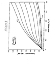
- the output characteristic of the MISFET 100 is shown in Figure 6 . It comprises nine graphs such as 160 and 162 indicating the variation of drain current I d with drain voltage V ds at constant gate voltage V gs from -0.2 V to 1.4 V in steps of 0.2 V between adjacent graphs. It can be seen that the drain current starts to saturate at a drain voltage of about 0.15 V, as indicated by a slight knee in each graph; this is a very low voltage for saturation to initiate, and it is due broadly speaking to the electron mobility in InSb being very high. It is advantageous because it implies that the MISFET 100 will have low power requirements.
- the output characteristic is generally of the classical form for MISFETs, which is evidence that a viable MISFET has been produced. At a drain voltage V ds of 0.3 V the drain current is switchable between about 10 and 110 mAmm -1 by changing the gate voltage V gs from -0.2 to 1.2 V.
- the transfer characteristic of the MISFET 100 is shown in Figure 7 . It comprises five graphs such as 170 and 172 indicating the variation of transconductance g m with gate voltage V gs at constant drain voltage. The drain voltage changes between adjacent graphs from 0.1 V to 0.5 V in steps of 0.1 V. It can be seen that the maximum DC transconductance of the MISFET 100 is about 120 mS mm -1 , and the threshold gate voltage is about 0.4 V.
- the leakage pedestal of the MISFET 100 is about 8 mA mm -1 , as shown by the intercept on the current axis in Figure 6 .
- the maximum drain currents are about 120 mA mm -1 , determined by the drain current ceasing to increase with gate voltage.
- the device starts to break down slowly at a drain voltage of around 0.5 V as indicated by the upward curvature of the current/voltage graphs at high drain voltage; this is due to band-to-band tunnelling and surface leakage (probably surface tunnelling generation), both of which it is possible to reduce.
- the MISFET 100 had a significant resistance in series with the channel, of about 2.5 Ohm on each side, measured by forward biasing the base-source/drain diodes. This is believed mainly to be due to the contacting process, and will reduce the transconductances (and hence f T ) below ideal values.
- the AC parameters of the MISFET 100 are shown in Figure 9 .
- the measured current gain cut-off frequency, f T is 74 GHz - as far as is known at present this is the highest f T measured for any FET with 0.7 ⁇ m gate length irrespective of transistor type or material. It is more than a factor of four greater than the best value (17 GHz) obtained for any of prior art devices 10 produced for investigation purposes, and more than a factor of seven greater than the typical value (10 GHz) for these devices. It should be possible to increase f T further by reducing the resistance in series with the channel.
- the frequency f max at which the unilateral power gain falls to unity is 89 GHz; this is limited by the channel series resistance, and by the output conductance which is relatively low at present.
- Modelled results for an implanted enhancement-mode MISFET structures similar to that shown in Figure 3 but with gate lengths of 1 ⁇ m and 0.25 ⁇ m are shown in the following Table 3, which provides theoretically attainable values for maximum g m , f T and f max .
- the values for 0.25 ⁇ m gate length assume the gate insulator oxide thickness to be scaled by the same factor as the gate length.
- Table 2 Modelled Parameters for Enhancement-mode MISFETs of the Invention Gate Length 1.0 ⁇ m 0.25 ⁇ m Maximum g m 188 mS mm -1 500 mS mm -1 Current Gain Cut-off Frequency f T 68 GHz 185 GHz Unity Unilateral Power Gain Frequency f max 202 GHz 264 GHz
- Combinations of materials that may be used to produce FETs of the invention include PbSe/PbS, In l-y Al y Sb/In l-x Al x Sb, InAs/InAs l-x P x , InAs l-x Sb x /In l-y AlySb, InAs l-x Sb x /InAs l-y P y , GaAs/Ga l-x Al x As, In l-x Ga x sb/In l-y mAl y Sb and Hg l-x Cd x Te/Hg l-y Cd y Te.
- Values of the composition parameters x, or x and y must be suitably chosen.
- the MISFET consisted of InSb/In l-x Al x Sb, which is a special case of the second of these with the parameter y equal to zero.
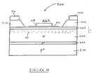
- a depletion mode MISFET of the invention is indicated generally by 200. It comprises a weakly doped p-type InSb substrate (not shown) upon which are grown five successive layers 202, 204, 206, 208 and 210 having the following thicknesses and compositions:-
- the MISFET 200 may optionally include a buried p-type layer 211 (indicated by chain lines) within the intrinsic layer 206 to improve confinement of charge carriers near the gate insulation layer 210. It has n + source and drain regions 212 and 214 each approximately 0.2 ⁇ m thick with an Si dopant concentration of 2x10 18 cm -3 and forming extracting contacts to the channel layer 208. These regions provide carrier extraction in the intrinsic layer 206 via the channel layer 208.
- the MISFET 200 has source, gate and drain contacts 216, 218 and 220 consisting of successive Cr and Au layers (not shown). Except where indicated above, the MISFET 200 has dimensions similar to the enhancement mode device described earlier.
- the layers 202 to 208 were grown by molecular beam epitaxy (MBE).
- MBE molecular beam epitaxy
- the source and drain regions 212 and 214 were produced by MBE growth on the channel layer 208, the central region of the latter being masked to avoid growth upon it. After removal of this mask, the gate insulation layer 210 and electrode 218 are deposited.
- the source and drain regions 212 and 214 define between them a gate recess 222 within which the gate insulation layer 210 and gate contact 218 are located supported by the channel layer 208.
- the recess may be more or less deep than the height of the gate electrode 218.
- the gate recess 222 is not a groove produced by etching as in the prior art, but instead a recess defined by growth of upstanding sides. In consequence the formation of the recess 222 does not imply problems associated with too deep a groove affecting channel shape.
- the fifth layer 210 consisted of 40 nm of sputtered SiO 2 deposited on top of 30 nm of anodic oxide.
- the gate contact 218 extends over most of that part of the channel layer 208 which is between the source and drain regions 212 and 214; the degree to which it does this is not very critical because it is merely required for modulation/depletion of an existing device channel, as opposed to establishment of a complete channel between source and drain which is required in an enhancement mode device.
- the MISFET 200 employs a channel layer 208 to provide an accessible source of electrons; the latter in turn provides a conducting path from source 212 to drain 214 depletable of charge carriers by the gate electrode potential.
- This path may be entirely within the channel layer 208 or the intrinsic layer 206 or may be partly in one of these and partly in the other.
- the threshold voltage of the MISFET 200 is determined by the doping per unit area of the channel layer 208, ie the product of the layer thickness and depletable of charge carriers by the gate electrode potential. This path may be entirely within the channel layer 208 or the intrinsic layer 206 or may be partly in one of these and partly in the other.
- the threshold voltage of the MISFET 200 is determined by the doping per unit area of the channel layer 208, ie the product of the layer thickness and its doping per unit volume.
- the channel layer 208 extends substantially along the direction of the electric field produced by the source-drain voltage in the absence of a gate voltage. This layer is not U-shaped to any unacceptable degree; ie any concavity or convexity in this layer is less than 50 nm in extent.
- Modelled - ie theoretical - performance figures were obtained for the depletion-mode MISFET 200 assuming that the gate insulation oxide thickness was equal to that in the device 100. These figures are shown in Table 3 as follows: Table 3: Modelled Parameters for Depletion-mode MISFETs of the Invention Gate Length 1.0 ⁇ m 0.25 ⁇ m Maximum g m 190 mS mm -1 590 mS mm -1 Current Gain Cut-off Frequency f T 68 GHz 220 GHz Unity Unilateral Power Gain Frequency f max 164 GHz 377 GHz
- current gain cut-off frequency f T (GHz) is shown as a function of gate length ( ⁇ m) for a variety of device technologies, actual or modelled, as follows: InSb ideal - (calculated from gate length and carrier velocity only), modelled InSb enhancement and depletion mode MISFETs, the InSb enhancement mode MISFET 100, InP- and GaAs-based HEMTs and silicon NMOS.
- the MISFET 200 may have a different form of channel.
- the 20 nm thick channel layer 208 may be replaced by a 3 nm thick InSb channel layer with a Si dopant concentration of 2x10 18 cm -3 separated from the gate oxide layer 210 by a ⁇ InSb layer 20 nm thick with a dopant concentration of 1x10 15 cm -3 .
- This is equivalent to the channel layer being reduced in thickness and buried in the intrinsic ⁇ layer 206, and is estimated to give a 30% operating speed enhancement.
- the source and drain regions 212 and 214 form extracting contacts with the intrinsic layer 206.
- the characteristic 250 corresponds to a device containing a lower Shockley/Read trap density than is currently attainable.
- the device is a p + p + ⁇ n + diode structure which is reverse biased in operation, ie it has a base layer which is biased negative with respect to its source region. Under this bias, carrier extraction and exclusion take place in the intrinsic layer, from which electrons (minority carriers) are removed by an associated ⁇ n + junction acting as an extracting contact.
- the slope of the I B V BS characteristic 250 is zero, indicating infinite differential impedance.
- the variation of gate threshold voltage with base bias voltage V BS - referred to as "back gating" - is minimised, and so this is the preferred operating point for base bias.
- the modelled results referred to above come from drift-diffusion simulation and neglect ballistic effects, which are expected to become significant at gate lengths of around 0.5 ⁇ m.
- the effect of this will be to increase the average saturation velocity, and hence the g m and f T leading to potential for greater improvements in performance.
- Transistors of the invention are potentially applicable to high-speed analogue device applications. If grown on a semi-insulating substrate or virtual substrate, they could be used in microwave integrated circuits.
- An InSb device is operative at low voltage, less than 0.5 V, and is therefore characterised by low power consumption which is extremely useful for hand-held applications, providing longer battery lifetimes. Also, it has high electron velocity which allows higher ultimate frequencies to be reached, or alternatively provides the required operating speed at a longer gate length, making it more robust.
- Transistors of the invention may also be used as digital devices, especially for low-complexity circuits. They are very attractive for high-speed low-power applications because they potentially have a very low P ⁇ product, where P is energy dissipated in a switching operation and ⁇ is the time to switch.
- the invention provides FETs which are fast, have low power dissipation and exploit the inherent high electron mobility and saturation velocity of InSb/In 1-x Al x Sb. These FETs give high-speed, low-power performance and demonstrate off-state leakage currents which are well below levels normally associated with InSb/In 1-x Al x Sb, due to the incorporation of carrier exclusion and extraction techniques. MISFETs of the invention with 0.7 ⁇ m gate length have the highest f T value yet reported for this gate length, and further improvements in both speed and off-state leakage are expected to be obtainable.
Landscapes
- Insulated Gate Type Field-Effect Transistor (AREA)
- Junction Field-Effect Transistors (AREA)
Claims (11)
- Transistor à effet de champ (FET) du type comprenant une zone (106) présentant une conductivité intrinsèque lorsque non polarisée à une température d'exploitation du transistor FET et un moyen de polarisation pour réduire la contribution intrinsèque à la concentration en porteurs de charge dans la zone intrinsèque (106), le transistor FET étant un transistor FET à métal insolant semi-conducteur à mode d'enrichissement ;
dans lequel le transistor FET (100) inclut en outre un moyen pour définir un canal s'étendant entre une zone source (110) et une zone de drain (112), avec un écart intermédiaire par rapport à la rectitude de canal qui n'est pas supérieur à 50 nm en étendue, tel qu'approprié pour permettre l'obtention d'une valeur élevée de fréquence de coupure de gain en courant ; et
dans lequel la zone intrinsèque (106) présente une interface avec une zone de barrière (104) présentant elle-même une interface avec une zone de base (102), et dans lequel les zones de base, de barrière et intrinsèque (106, 104, 102) sont d'un même type de conductivité, et la zone de barrière (104) est d'une largeur de bande interdite plus élevée que les zones de base et intrinsèque (106, 102) et fournit un contact d'exclusion à la zone intrinsèque (106); et
dans lequel les zones de base, de barrière et intrinsèque (102, 104, 106) sont agencées successivement dans une structure en couches, et la zone intrinsèque (106) présente une partie de surface plane prenant en charge une couche d'isolation de grille (108) et un contact de grille (116) ; et
dans lequel la zone intrinsèque (106) est de type p et forme un moyen de contact d'extraction en combinaison avec les zones de drain et source (110, 112) ; et
dans lequel :a) la zone de base (102) est constituée de p+ InSb et présente une concentration en accepteurs d'au moins 5 x 1017 cm-3 :b) la zone de barrière (104) est constituée de p+ In1-xAlxSb, où x est dans la plage de 0,05 à 0,25 et présente une concentration en accepteurs d'au moins 5 x 1017 cm-3;c) la zone intrinsèque (106) est constituée de π InSb avec une concentration en accepteurs intérieure à 5 x 1017 cm-3; etd) les zones de drain et source (110, 112) sont constituées de n+InSb avec une concentration en dopants d'au moins 5 x 1017 cm-3. - Transistor FET selon la revendication 1, caractérisé en ce qu'un écart quelconque par rapport à la rectitude de canal n'est pas supérieur à 5 nm en étendue.
- Transistor FET selon la revendication 1 ou 2, caractérisé en ce qu'il intègre des zones de drain et source (110, 112) qui sont de type n fortement dopé.
- Transistor FET selon l'une quelconque des revendications 1 à 3, caractérisé en ce qu'il inclut un contact de grille (116) isolé de, et s'étendant sur la partie de la zone intrinsèque (106) entre les zones de drain et source (110, 112), en vue de définir entre elles un canal d'enrichissement en fonctionnement.
- Transistor à effet de champ (FET) du type comprenant une zone (206) présentant une conductivité intrinsèque lorsque polarisée à une température d'exploitation du transistor FET et un moyen de polarisation pour réduire la contribution intrinsèque à la concentration en porteurs de charge dans la zone intrinsèque (206), le transistor FET étant un transistor FET à métal isolant semi-conducteur à mode d'appauvrissement (200) présentant une zone de canal associée (208) ;
dans lequel le transistor FET (200) inclut en outre un moyen pour définir un canal s'étendant entre une zone source (212) et une zone de drain (214), avec un écart intermédiaire par rapport à la rectitude de canal qui n'est pas supérieur à 50 nm en étendue, tel qu'approprié pour permettre l'obtention d'une valeur élevée de fréquence de coupure de gain en courant ; et
dans lequel la zone intrinsèque (206) présente une interface avec une zone de barrière (204) présentant elle-même une interface avec une zone de base (202), et dans lequel les zones de base, de barrière et intrinsèque (206, 204, 202) sont d'un même type de conductivité, et la zone de barrière (204) est d'une largeur de bande interdite plus élevée que les zones de base et intrinsèque (206, 202) et fournit un contact d'exclusion à la zone intrinsèque (206) ; et
dans lequel la zone intrinsèque (206) prend en charge la zone de canal (208), les zones de base, de barrière, de canal et intrinsèque (202, 204, 206, 208) sont agencées successivement dans une structure en couches, les zones de drain et source (212, 214) sont en appui sur la zone de canal (208), et la zone de canal (208) présente une partie de surface sensiblement plane prenant en charge une couche d'isolation de grille (210) et un contact de grille (218) ; et dans lequel la zone intrinsèque (206) est de type p et forme, ou la zone de canal (208) forme, un moyen de contact d'extraction avec les zones de drain et source (212, 214) ; et
dans lequel :a) la zone de base (202) est constituée de p+ InSb et présente une concentration en accepteurs d'au moins 5 x 1017 cm-3:b) la zone de barrière (204) est constituée de p+ In1-xAlxSb , où x est dans la plage de 0,05 à 0,25 et présente une concentration en accepteurs d'au moins 5 x 1017 cm-3;c) la zone intrinsèque (206) est constituée de π InSb avec une concentration en accepteurs inférieure à 5 x 1017 cm-3; etd) les zones de drain et source (212, 214) sont constituées de n+InSb avec une concentration en dopants d'au moins 5 x 1017 cm-3. - Transistor FET selon la revendication 5, caractérisé en ce qu'un écart quelconque par rapport à la rectitude de canal n'est pas supérieur à 5 nm en étendue.
- Transistor FET selon la revendication 5 ou 6, caractérisé en ce qu'il intègre des zones de drain et source (212, 214) qui représentent des excroissances fortement dopées formées sur la zone intrinsèque (206) ou sur la zone de canal (208), les excroissances définissant entre elles un évidemment de grille (222) recevant un contact de grille (218).
- Transistor FET selon l'une quelconque des revendications 5 à 7, caractérisé en ce que les zones de drain et source (212, 214) définissent entre elles un évidemment de grille (222), la zone de canal (208) présente une partie de surface au niveau d'une extrémité de l'evidemment (222) prenant en charge une couche d'isolation de grille (208) et un contact de grille (210).
- Transistor FET selon l'une quelconque des revendications 5 à 8, caractérisé en ce que la zone de canal se situe entre des partiels de la zone intrinsèque et en ce que cette dernière forme un moyen de contact d'extraction en combinaison avec les zones de drain et source (212, 214).
- Transistor FET selon la revendication 9, caractérise en ce que la zone intrinsèque (206) contient la zone de canal (208), les zones de drain et source (212, 214) sont prises en charge par la zone intrinsèque (206) et définissent entre elles un évidemment de grille (222), et la zone intrinsèque (206) présente une partie de surface au niveau d'une extrémité de l'évidemment (222) prenant en charge une couche d'isolation de grille (208) et un contact de grille (210).
- Transistor FET selon l'une quelconque des revendications précédentes, caractérisé en ce que le moyen de polarisation destiné à réduire la contribution intrinsèque à la concentration en porteurs de charge dans la zone intrinsèque (106, 206) est agencé de manière à polariser le transistor FET (100, 200) au niveau d'un point d'impédance différentielle infinie où la variation de tension seuil de grille avec les variations de tension de polarisation du substrat est minimisée.
Applications Claiming Priority (3)
| Application Number | Priority Date | Filing Date | Title |
|---|---|---|---|
| GB9725189 | 1997-11-28 | ||
| GB9725189A GB2331841A (en) | 1997-11-28 | 1997-11-28 | Field effect transistor |
| PCT/GB1998/001695 WO1999028975A1 (fr) | 1997-11-28 | 1998-06-10 | Transistor a effet de champ |
Publications (2)
| Publication Number | Publication Date |
|---|---|
| EP1034568A1 EP1034568A1 (fr) | 2000-09-13 |
| EP1034568B1 true EP1034568B1 (fr) | 2013-03-13 |
Family
ID=10822789
Family Applications (1)
| Application Number | Title | Priority Date | Filing Date |
|---|---|---|---|
| EP98928446A Expired - Lifetime EP1034568B1 (fr) | 1997-11-28 | 1998-06-10 | Transistor a effet de champ |
Country Status (8)
| Country | Link |
|---|---|
| US (1) | US6624451B2 (fr) |
| EP (1) | EP1034568B1 (fr) |
| JP (3) | JP2001525615A (fr) |
| KR (1) | KR100542963B1 (fr) |
| CN (1) | CN1284204A (fr) |
| CA (1) | CA2311778C (fr) |
| GB (2) | GB2331841A (fr) |
| WO (1) | WO1999028975A1 (fr) |
Families Citing this family (20)
| Publication number | Priority date | Publication date | Assignee | Title |
|---|---|---|---|---|
| GB2362506A (en) * | 2000-05-19 | 2001-11-21 | Secr Defence | Field effect transistor with an InSb quantum well and minority carrier extraction |
| US7226843B2 (en) * | 2002-09-30 | 2007-06-05 | Intel Corporation | Indium-boron dual halo MOSFET |
| US6995473B2 (en) * | 2002-12-19 | 2006-02-07 | Matsushita Electric Industrial Co., Ltd. | Stacked semiconductor transistors |
| US7288821B2 (en) * | 2005-04-08 | 2007-10-30 | International Business Machines Corporation | Structure and method of three dimensional hybrid orientation technology |
| JP2007115971A (ja) * | 2005-10-21 | 2007-05-10 | Fujitsu Ltd | 半導体装置とその製造方法 |
| DE102006030631B4 (de) * | 2006-07-03 | 2011-01-05 | Infineon Technologies Austria Ag | Halbleiterbauelementanordnung mit einem Leistungsbauelement und einem Logikbauelement |
| KR100847827B1 (ko) * | 2006-12-29 | 2008-07-23 | 동부일렉트로닉스 주식회사 | 고전압 트랜지스터의 제조 방법 |
| US8017915B2 (en) | 2008-03-14 | 2011-09-13 | Reflexion Medical, Inc. | Method and apparatus for emission guided radiation therapy |
| US8735903B2 (en) * | 2010-02-10 | 2014-05-27 | Taiwan Semiconductor Manufacturing Company, Ltd. | Density of states engineered field effect transistor |
| US20140217470A1 (en) * | 2011-09-08 | 2014-08-07 | Tamura Corporation | Ga2O3 SEMICONDUCTOR ELEMENT |
| US8803242B2 (en) * | 2011-09-19 | 2014-08-12 | Eta Semiconductor Inc. | High mobility enhancement mode FET |
| US8891573B2 (en) | 2012-05-14 | 2014-11-18 | Arizona Board Of Regents | 6.1 angstrom III-V and II-VI semiconductor platform |
| EP3221050B1 (fr) * | 2014-11-18 | 2021-05-19 | Avidien Technologies, Inc. | Pipette à déplacement d'air à canaux multiples |
| CN110234275B (zh) | 2016-11-15 | 2023-08-22 | 反射医疗公司 | 用于发射引导式高能光子传输的系统 |
| WO2018183748A1 (fr) | 2017-03-30 | 2018-10-04 | Reflexion Medical, Inc. | Systèmes et procédés de radiothérapie avec suivi de tumeur |
| WO2019014387A1 (fr) | 2017-07-11 | 2019-01-17 | Reflexion Medical, Inc. | Procédés de gestion de rémanence pour détecteur tep |
| WO2019032911A1 (fr) | 2017-08-09 | 2019-02-14 | Reflexion Medical, Inc. | Systèmes et procédés de détection de défaut dans une radiothérapie guidée par émission |
| US11369806B2 (en) | 2017-11-14 | 2022-06-28 | Reflexion Medical, Inc. | Systems and methods for patient monitoring for radiotherapy |
| US11239802B2 (en) | 2019-10-02 | 2022-02-01 | Wolfspeed, Inc. | Radio frequency transistor amplifiers having engineered instrinsic capacitances for improved performance |
| US11798983B2 (en) | 2021-07-19 | 2023-10-24 | United Semiconductor Japan Co., Ltd. | Semiconductor device with deeply depleted channel and manufacturing method thereof |
Citations (2)
| Publication number | Priority date | Publication date | Assignee | Title |
|---|---|---|---|---|
| US4452646A (en) * | 1981-09-28 | 1984-06-05 | Mcdonnell Douglas Corporation | Method of making planar III-V compound device by ion implantation |
| WO1990006595A1 (fr) * | 1988-12-09 | 1990-06-14 | Hughes Aircraft Company | Transistor a effet de champ mos de grandeur inferieure au micron et a couche ultrafine avec canal intrinseque |
Family Cites Families (10)
| Publication number | Priority date | Publication date | Assignee | Title |
|---|---|---|---|---|
| US4080721A (en) * | 1975-06-30 | 1978-03-28 | International Business Machines Corporation | Fabrication of semiconductor device |
| DE3018988A1 (de) * | 1980-05-17 | 1981-11-26 | Deutsche Itt Industries Gmbh, 7800 Freiburg | Isolierschicht-feldeffekttransistor |
| JPS5710269A (en) * | 1980-12-22 | 1982-01-19 | Itt | Insulated gate type field effect transistor |
| JP2515751B2 (ja) * | 1986-08-13 | 1996-07-10 | 株式会社日立製作所 | 超伝導トランジスタ |
| US4927782A (en) * | 1989-06-27 | 1990-05-22 | The United States Of America As Represented By The Secretary Of The Navy | Method of making self-aligned GaAs/AlGaAs FET's |
| GB9100351D0 (en) * | 1991-01-08 | 1991-02-20 | Secr Defence | Semiconductor heterostructure device |
| US5329137A (en) * | 1991-07-17 | 1994-07-12 | The United States Of America As Represented By The Secretary Of The Air Force | Integrated total internal reflection optical switch utilizing charge storage in a quantum well |
| TW215967B (en) * | 1992-01-17 | 1993-11-11 | Seiko Electron Co Ltd | MOS Poly-Si thin film transistor with a flattened channel interface and method of producing same |
| JPH06267991A (ja) * | 1993-03-12 | 1994-09-22 | Hitachi Ltd | 半導体装置およびその製造方法 |
| KR970000538B1 (ko) * | 1993-04-27 | 1997-01-13 | 엘지전자 주식회사 | 게이트 리세스 구조를 갖는 전계효과트랜지스터의 제조방법 |
-
1997
- 1997-11-28 GB GB9725189A patent/GB2331841A/en not_active Withdrawn
-
1998
- 1998-06-10 JP JP2000523711A patent/JP2001525615A/ja active Pending
- 1998-06-10 CN CN98813383A patent/CN1284204A/zh active Pending
- 1998-06-10 WO PCT/GB1998/001695 patent/WO1999028975A1/fr not_active Ceased
- 1998-06-10 EP EP98928446A patent/EP1034568B1/fr not_active Expired - Lifetime
- 1998-06-10 GB GB0011379A patent/GB2346481B/en not_active Expired - Fee Related
- 1998-06-10 CA CA002311778A patent/CA2311778C/fr not_active Expired - Fee Related
- 1998-06-10 KR KR1020007005781A patent/KR100542963B1/ko not_active Expired - Fee Related
-
2001
- 2001-05-21 US US09/860,770 patent/US6624451B2/en not_active Expired - Lifetime
-
2009
- 2009-04-14 JP JP2009097671A patent/JP2009194392A/ja active Pending
-
2010
- 2010-12-03 JP JP2010269978A patent/JP5325198B2/ja not_active Expired - Lifetime
Patent Citations (2)
| Publication number | Priority date | Publication date | Assignee | Title |
|---|---|---|---|---|
| US4452646A (en) * | 1981-09-28 | 1984-06-05 | Mcdonnell Douglas Corporation | Method of making planar III-V compound device by ion implantation |
| WO1990006595A1 (fr) * | 1988-12-09 | 1990-06-14 | Hughes Aircraft Company | Transistor a effet de champ mos de grandeur inferieure au micron et a couche ultrafine avec canal intrinseque |
Non-Patent Citations (1)
| Title |
|---|
| Retrieved from the Internet <URL:http://www.electropedia.org/iev/iev.nsf/display?openform&ievref=521-02-07> [retrieved on 20080811] * |
Also Published As
| Publication number | Publication date |
|---|---|
| GB2331841A (en) | 1999-06-02 |
| CN1284204A (zh) | 2001-02-14 |
| GB2331841A9 (en) | |
| GB2346481A (en) | 2000-08-09 |
| JP2011049599A (ja) | 2011-03-10 |
| JP5325198B2 (ja) | 2013-10-23 |
| JP2001525615A (ja) | 2001-12-11 |
| US6624451B2 (en) | 2003-09-23 |
| GB2346481B (en) | 2002-11-20 |
| US20020014633A1 (en) | 2002-02-07 |
| GB0011379D0 (en) | 2000-06-28 |
| CA2311778A1 (fr) | 1999-06-10 |
| CA2311778C (fr) | 2006-05-30 |
| EP1034568A1 (fr) | 2000-09-13 |
| KR20010032538A (ko) | 2001-04-25 |
| JP2009194392A (ja) | 2009-08-27 |
| GB9725189D0 (en) | 1998-01-28 |
| WO1999028975A1 (fr) | 1999-06-10 |
| KR100542963B1 (ko) | 2006-01-20 |
Similar Documents
| Publication | Publication Date | Title |
|---|---|---|
| EP1034568B1 (fr) | Transistor a effet de champ | |
| Hill et al. | Enhancement-mode GaAs MOSFETs with an In0. 3 Ga0. 7As channel, a mobility of over 5000 cm2/V· s, and transconductance of over 475 μS/μm | |
| US4830980A (en) | Making complementary integrated p-MODFET and n-MODFET | |
| US4471366A (en) | Field effect transistor with high cut-off frequency and process for forming same | |
| EP2362422A2 (fr) | Dispositif semi-conducteur vertical de puissance et sa méthode de fabrication | |
| US10483360B2 (en) | Semiconductor device comprising a gradually increasing field dielectric layer and method of manufacturing a semiconductor device | |
| GB2285175A (en) | High electron mobility transistor | |
| Passlack et al. | Implant-free high-mobility flatband MOSFET: Principles of operation | |
| Ashley et al. | High-speed, low-power InSb transistors | |
| US20080157117A1 (en) | Insulated gate bipolar transistor with enhanced conductivity modulation | |
| EP0717448A1 (fr) | Dispositif MOS à faible puissance asymétrique | |
| Lour et al. | Comparisons between mesa-and airbridge-gate AlGaAs/InGaAs doped-channel field-effect transistors | |
| EP0317345B1 (fr) | Transistor à effet de champ | |
| Daniels et al. | Doped channel pseudomorphic GaAs/InGaAs/AlGaAs hetero-structure FETs | |
| JPH08255898A (ja) | 半導体装置 | |
| EP0283878A1 (fr) | Transistor à effet de champ | |
| JPS61116875A (ja) | 半導体装置 | |
| Abid et al. | Direct-Schottky-contact InP MESFET | |
| Rieh | Semiconductor Technologies for THz Applications | |
| Hill et al. | Enhancement-Mode GaAs MOSFETs With an $\hbox {In} _ {0.3}\hbox {Ga} _ {0.7}\hbox {As} $ Channel, a Mobility of Over 5000$\hbox {cm}^{2}/\hbox {V}\cdot\hbox {s} $, and Transconductance of Over 475$\mu\hbox {S}/\mu\hbox {m} $ | |
| Ho et al. | Fabrication of $\hbox {Si} _ {1-x}\hbox {Ge} _ {x}/\hbox {Si} $ pMOSFETs Using Corrugated Substrates for Improved $ I_ {\rm ON} $ and Reduced Layout-Width Dependence | |
| Girard et al. | Evaluation of currents in the fA range | |
| Chan et al. | In0. 52Al0. 48As/In0. 53Ga0. 47As higfets using novel 0.2 μm self-aligned T-gate technology | |
| JPH05102190A (ja) | 化合物半導体ヘテロ接合ゲート電界効果トランジスタ | |
| Zhang et al. | InGaN/GaN/AlGaN RTD with Inherent Extreme Low Leakage Current & High Current Rising Rate |
Legal Events
| Date | Code | Title | Description |
|---|---|---|---|
| PUAI | Public reference made under article 153(3) epc to a published international application that has entered the european phase |
Free format text: ORIGINAL CODE: 0009012 |
|
| 17P | Request for examination filed |
Effective date: 20000513 |
|
| AK | Designated contracting states |
Kind code of ref document: A1 Designated state(s): DE FI FR GB IE IT NL SE |
|
| RAP1 | Party data changed (applicant data changed or rights of an application transferred) |
Owner name: QINETIQ LIMITED |
|
| 17Q | First examination report despatched |
Effective date: 20060406 |
|
| RBV | Designated contracting states (corrected) |
Designated state(s): DE FI FR IE IT NL SE |
|
| RAP1 | Party data changed (applicant data changed or rights of an application transferred) |
Owner name: QINETIQ LIMITED |
|
| REG | Reference to a national code |
Ref country code: DE Ref legal event code: R079 Ref document number: 69842976 Country of ref document: DE Free format text: PREVIOUS MAIN CLASS: H01L0029780000 Ipc: H01L0029100000 |
|
| RIC1 | Information provided on ipc code assigned before grant |
Ipc: H01L 29/205 20060101ALI20121002BHEP Ipc: H01L 29/78 20060101ALI20121002BHEP Ipc: H01L 29/10 20060101AFI20121002BHEP Ipc: H01L 29/66 20060101ALI20121002BHEP |
|
| GRAP | Despatch of communication of intention to grant a patent |
Free format text: ORIGINAL CODE: EPIDOSNIGR1 |
|
| GRAS | Grant fee paid |
Free format text: ORIGINAL CODE: EPIDOSNIGR3 |
|
| GRAA | (expected) grant |
Free format text: ORIGINAL CODE: 0009210 |
|
| AK | Designated contracting states |
Kind code of ref document: B1 Designated state(s): DE FI FR IE IT NL SE |
|
| REG | Reference to a national code |
Ref country code: IE Ref legal event code: FG4D |
|
| REG | Reference to a national code |
Ref country code: DE Ref legal event code: R096 Ref document number: 69842976 Country of ref document: DE Effective date: 20130508 |
|
| REG | Reference to a national code |
Ref country code: NL Ref legal event code: T3 |
|
| PG25 | Lapsed in a contracting state [announced via postgrant information from national office to epo] |
Ref country code: SE Free format text: LAPSE BECAUSE OF FAILURE TO SUBMIT A TRANSLATION OF THE DESCRIPTION OR TO PAY THE FEE WITHIN THE PRESCRIBED TIME-LIMIT Effective date: 20130313 |
|
| PG25 | Lapsed in a contracting state [announced via postgrant information from national office to epo] |
Ref country code: FI Free format text: LAPSE BECAUSE OF FAILURE TO SUBMIT A TRANSLATION OF THE DESCRIPTION OR TO PAY THE FEE WITHIN THE PRESCRIBED TIME-LIMIT Effective date: 20130313 |
|
| REG | Reference to a national code |
Ref country code: NL Ref legal event code: V1 Effective date: 20140101 |
|
| PLBE | No opposition filed within time limit |
Free format text: ORIGINAL CODE: 0009261 |
|
| STAA | Information on the status of an ep patent application or granted ep patent |
Free format text: STATUS: NO OPPOSITION FILED WITHIN TIME LIMIT |
|
| 26N | No opposition filed |
Effective date: 20131216 |
|
| REG | Reference to a national code |
Ref country code: IE Ref legal event code: MM4A |
|
| REG | Reference to a national code |
Ref country code: DE Ref legal event code: R119 Ref document number: 69842976 Country of ref document: DE Effective date: 20140101 Ref country code: DE Ref legal event code: R097 Ref document number: 69842976 Country of ref document: DE Effective date: 20131216 |
|
| REG | Reference to a national code |
Ref country code: FR Ref legal event code: ST Effective date: 20140228 |
|
| PG25 | Lapsed in a contracting state [announced via postgrant information from national office to epo] |
Ref country code: NL Free format text: LAPSE BECAUSE OF NON-PAYMENT OF DUE FEES Effective date: 20140101 Ref country code: DE Free format text: LAPSE BECAUSE OF NON-PAYMENT OF DUE FEES Effective date: 20140101 Ref country code: IE Free format text: LAPSE BECAUSE OF NON-PAYMENT OF DUE FEES Effective date: 20130610 |
|
| PG25 | Lapsed in a contracting state [announced via postgrant information from national office to epo] |
Ref country code: FR Free format text: LAPSE BECAUSE OF NON-PAYMENT OF DUE FEES Effective date: 20130701 Ref country code: IT Free format text: LAPSE BECAUSE OF NON-PAYMENT OF DUE FEES Effective date: 20130610 |