EP1037280A2 - Configuration de cellules "mémoires" pour une intéraction réduite entre les noeuds de stockage et les transistors - Google Patents
Configuration de cellules "mémoires" pour une intéraction réduite entre les noeuds de stockage et les transistors Download PDFInfo
- Publication number
- EP1037280A2 EP1037280A2 EP00103617A EP00103617A EP1037280A2 EP 1037280 A2 EP1037280 A2 EP 1037280A2 EP 00103617 A EP00103617 A EP 00103617A EP 00103617 A EP00103617 A EP 00103617A EP 1037280 A2 EP1037280 A2 EP 1037280A2
- Authority
- EP
- European Patent Office
- Prior art keywords
- wordlines
- trench
- recited
- trenches
- gate
- Prior art date
- Legal status (The legal status is an assumption and is not a legal conclusion. Google has not performed a legal analysis and makes no representation as to the accuracy of the status listed.)
- Withdrawn
Links
- 230000015654 memory Effects 0.000 title claims abstract description 32
- 230000003993 interaction Effects 0.000 title description 6
- 238000009792 diffusion process Methods 0.000 claims abstract description 19
- 239000000758 substrate Substances 0.000 claims abstract description 17
- 239000004065 semiconductor Substances 0.000 description 9
- 239000002019 doping agent Substances 0.000 description 8
- 230000000694 effects Effects 0.000 description 8
- 239000003990 capacitor Substances 0.000 description 6
- 230000006870 function Effects 0.000 description 3
- 238000002955 isolation Methods 0.000 description 2
- 230000009471 action Effects 0.000 description 1
- 230000004048 modification Effects 0.000 description 1
- 238000012986 modification Methods 0.000 description 1
Images


Classifications
-
- G—PHYSICS
- G11—INFORMATION STORAGE
- G11C—STATIC STORES
- G11C11/00—Digital stores characterised by the use of particular electric or magnetic storage elements; Storage elements therefor
- G11C11/21—Digital stores characterised by the use of particular electric or magnetic storage elements; Storage elements therefor using electric elements
- G11C11/34—Digital stores characterised by the use of particular electric or magnetic storage elements; Storage elements therefor using electric elements using semiconductor devices
- G11C11/40—Digital stores characterised by the use of particular electric or magnetic storage elements; Storage elements therefor using electric elements using semiconductor devices using transistors
- G11C11/401—Digital stores characterised by the use of particular electric or magnetic storage elements; Storage elements therefor using electric elements using semiconductor devices using transistors forming cells needing refreshing or charge regeneration, i.e. dynamic cells
-
- H—ELECTRICITY
- H10—SEMICONDUCTOR DEVICES; ELECTRIC SOLID-STATE DEVICES NOT OTHERWISE PROVIDED FOR
- H10B—ELECTRONIC MEMORY DEVICES
- H10B12/00—Dynamic random access memory [DRAM] devices
- H10B12/30—DRAM devices comprising one-transistor - one-capacitor [1T-1C] memory cells
- H10B12/37—DRAM devices comprising one-transistor - one-capacitor [1T-1C] memory cells the capacitor being at least partially in a trench in the substrate
-
- H—ELECTRICITY
- H10—SEMICONDUCTOR DEVICES; ELECTRIC SOLID-STATE DEVICES NOT OTHERWISE PROVIDED FOR
- H10B—ELECTRONIC MEMORY DEVICES
- H10B12/00—Dynamic random access memory [DRAM] devices
- H10B12/30—DRAM devices comprising one-transistor - one-capacitor [1T-1C] memory cells
- H10B12/48—Data lines or contacts therefor
-
- H—ELECTRICITY
- H10—SEMICONDUCTOR DEVICES; ELECTRIC SOLID-STATE DEVICES NOT OTHERWISE PROVIDED FOR
- H10D—INORGANIC ELECTRIC SEMICONDUCTOR DEVICES
- H10D89/00—Aspects of integrated devices not covered by groups H10D84/00 - H10D88/00
- H10D89/10—Integrated device layouts
-
- Y—GENERAL TAGGING OF NEW TECHNOLOGICAL DEVELOPMENTS; GENERAL TAGGING OF CROSS-SECTIONAL TECHNOLOGIES SPANNING OVER SEVERAL SECTIONS OF THE IPC; TECHNICAL SUBJECTS COVERED BY FORMER USPC CROSS-REFERENCE ART COLLECTIONS [XRACs] AND DIGESTS
- Y10—TECHNICAL SUBJECTS COVERED BY FORMER USPC
- Y10S—TECHNICAL SUBJECTS COVERED BY FORMER USPC CROSS-REFERENCE ART COLLECTIONS [XRACs] AND DIGESTS
- Y10S257/00—Active solid-state devices, e.g. transistors, solid-state diodes
- Y10S257/906—Dram with capacitor electrodes used for accessing, e.g. bit line is capacitor plate
-
- Y—GENERAL TAGGING OF NEW TECHNOLOGICAL DEVELOPMENTS; GENERAL TAGGING OF CROSS-SECTIONAL TECHNOLOGIES SPANNING OVER SEVERAL SECTIONS OF THE IPC; TECHNICAL SUBJECTS COVERED BY FORMER USPC CROSS-REFERENCE ART COLLECTIONS [XRACs] AND DIGESTS
- Y10—TECHNICAL SUBJECTS COVERED BY FORMER USPC
- Y10S—TECHNICAL SUBJECTS COVERED BY FORMER USPC CROSS-REFERENCE ART COLLECTIONS [XRACs] AND DIGESTS
- Y10S257/00—Active solid-state devices, e.g. transistors, solid-state diodes
- Y10S257/907—Folded bit line dram configuration
-
- Y—GENERAL TAGGING OF NEW TECHNOLOGICAL DEVELOPMENTS; GENERAL TAGGING OF CROSS-SECTIONAL TECHNOLOGIES SPANNING OVER SEVERAL SECTIONS OF THE IPC; TECHNICAL SUBJECTS COVERED BY FORMER USPC CROSS-REFERENCE ART COLLECTIONS [XRACs] AND DIGESTS
- Y10—TECHNICAL SUBJECTS COVERED BY FORMER USPC
- Y10S—TECHNICAL SUBJECTS COVERED BY FORMER USPC CROSS-REFERENCE ART COLLECTIONS [XRACs] AND DIGESTS
- Y10S257/00—Active solid-state devices, e.g. transistors, solid-state diodes
- Y10S257/908—Dram configuration with transistors and capacitors of pairs of cells along a straight line between adjacent bit lines
Definitions
- This disclosure relates to semiconductor layouts and more particularly, to a layout for reducing interaction between storage nodes and transistors in semiconductor memory cells.
- DRAM dynamic random access memories
- Semiconductor memories such as dynamic random access memories (DRAM) typically include memory cells with storage nodes. Generally these storage nodes are formed within deep trenches etched into substrates of the semiconductor memory chip. The storage nodes are accessed using an access transistor which allows charge to be stored in the storage node or retrieves charge from the storage depending on whether the desired action is a read or write function.
- dopant outdiffusion close to a wordline can cause problems such as short channel effects in the access transistor channel.
- Deep trench capacitors 10 are disposed under passing wordlines 12.
- Access transistors 14 are electrically coupled to storage nodes 16 of trench capacitors 10 through diffusion regions 18 which may be either a source or a drain of access transistors 14.
- Diffusion regions 20 are also included which are electrically connected to contacts 22.
- Contacts 22 connect to bitline (not shown) to read and write to storage nodes 16 through access transistors 14.
- Access transistors 14 are activated by wordlines 12. When voltage is applied to wordlines 12 a channel below wordline 12 conducts allowing current to flow between diffusion regions 18 and 20 and into or out of storage node 16.
- Wordlines 12 are preferably spaced across the smallest possible distance d to conserve layout area.
- the smallest possible distance is typically a minimum feature size F which is achievable by the technology.
- FIG. 2 a cross-sectional view of the layout of FIG. 1 is shown. Elements of FIG. 2 are labeled as described in FIG. 1.
- Storage nodes 16 are isolated from a doped well 24 by a dielectric collar 26. Shallow trench isolation 28 is provided over storage nodes 16 to electrically isolate the passing wordlines 12 formed above storage nodes 16.
- Diffusion regions 18 of access transistors 14 are connected to storage node 16 by a node diffusion region 30 to a buried strap 32. Node diffusion 30 and buried strap 32 are typically connected by outdiffusing dopants which mix to create a conductive region (node region 30) therebetween.
- the distance between wordlines 12 and buried strap 32 is usually 1F. But, if the overlay tolerance is considered, the dopant outdiffusion from buried strap 32 can potentially outdiffuse far enough to interact with a channel 34 below a gate 36 (wordline 12) causing short channel effects in access transistor 14.
- an overlay tolerance is F/2, i.e., a worst case distance is F/2.
- a length of channel 34 is a function of diffusion regions 18 and 20 and buried strap 32 outdiffusion. Also, it is a function of the overlay tolerance between wordlines 12 and deep trenches 10. If the dopant outdiffusion length form buried strap 32 is larger than F/2, the length of channel 34 becomes less than 1F. However, outdiffusion form buried strap 32 must generally be far enough (about F/2) to form a connection between diffusion region 18 and buried strap 32.
- a memory cell in accordance with the invention, includes a trench formed in a substrate, and an active area formed in the substrate below a gate and extending to the trench.
- the active area includes diffusion regions for forming a transistor for accessing a storage node in the trench, the transistor being activated by the gate.
- the gate defines a first axis wherein a portion of the active area extends transversely therefrom, the portion of the active area extending to the trench.
- the trench has a side closest to the portion of the active area, the side of the trench being angularly disposed relative to the gate such that a distance between the gate and the side of the trench is greater than a minimum feature size.
- a memory chip layout in accordance with the invention, includes trenches formed in a substrate, and active areas formed in the substrate.
- the active areas include diffusion regions for forming transistors for accessing storage nodes in the trenches.
- a plurality of wordlines is disposed substantially parallel to each other, the wordlines having a width and being spaced apart by a substantially same distance.
- the transistors each include a gate formed by the word lines, the word lines defining a first axis wherein a first portion of each active area extends transversely from below the wordline to a trench disposed below an adjacent wordline.
- the trenches have a side closest to the first portions of the active areas, the side closest of the trench being angularly disposed relative to the wordlines such that a distance between a wordline and a side closest to the first portion of a trench, disposed below an adjacent wordline, is greater than the substantially same distance between the wordlines.
- Another memory chip layout includes trenches, and active areas formed in a substrate, the active areas including diffusion regions for forming transistors for accessing storage nodes in the trenches.
- a plurality of wordlines are disposed substantially parallel to each other, the wordlines having a width and being spaced apart by a substantially same distance.
- the transistors each include a gate formed by the wordlines, the wordlines defining a first axis wherein a first portion of each active area extends transversely from below the wordline to a trench disposed below an adjacent wordline.
- the trenches have a side closest to the first portions of the active areas, the side closest to the first portions being angularly disposed relative to the word lines such that a distance between the wordline and the side closest to the first portions, disposed below an adjacent wordline, is greater than the substantially same distance between the wordlines.
- the active areas define a second axis which forms an angle with the wordlines and extends below two adjacent wordlines to connect to trenches at ends of the active areas.
- the trenches disposed below the two adjacent wordlines have at least on side aligned in a substantially parallel orientation relative to the second axis.
- the active areas may form an angle with the first axis such that a channel length of a channel of the access transistor disposed below the gate is greater than a width of the gate or wordlines.
- the trenches may have a shape including one of a rectangle, a trapezoid, a parallelogram and/or a bent rectangle.
- the portion (or first portion) of the active area may include a bend to further extend the distance between the gate and the side of the trench.
- the gate and/or the wordlines may include a width of greater than the minimum feature size to provide a longer channel length.
- the gate may include the width of greater than the minimum feature size only over the channels of the access transistors.
- the gate includes a width of the minimum feature size.
- the trenches below adjacent wordlines may be at least a minimum feature size apart. Pairs of wordlines adjacent on each side of the two wordlines may have active areas forming an angle opposite the rotation of the angles formed by active areas on the two wordlines, the trenches below the adjacent pairs having at least one side substantially parallel to the active areas of the adjacent pairs of wordlines and forming an angle opposite the rotation of the angles formed by active areas on the two wordlines.
- the present invention relates to semiconductor layouts and more particularly, to a layout for reducing interaction between storage nodes and transistors in semiconductor memory cells.
- the invention includes layouts for deep trench capacitors and active regions such that a greater distance between the storage node and the wordline below which exists a transistor channel is realized. By providing the additional distance between the buried strap and the wordline, outdiffusion from a buried strap into the channel may be prevented and short channel effects avoided.
- the invention further includes additional embodiments which provide increased distance between the buried strap and the wordline.
- the present invention is applicable to memory cells and in particular to dynamic random access memory (DRAM) cells. Other memory devices are also contemplated by the invention.
- DRAM dynamic random access memory
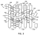
- Memory 100 includes deep trenches 102 and wordlines (gates) 104.
- Wordlines 104 are preferably spaced apart by a distance d, for example, the minimum feature size F. Further, wordlines preferably have a thickness of about F as well.
- Active areas 106 include a source region and a drain region on opposite side of each wordline 104. It is to be understood that the FIGS. include depictions of layouts with overlapping elements. These elements are provided on a plurality of different levels. For example, trenches are formed in a semiconductor substrate, active areas are diffused into the substrate and contacts and gate/wordlines are formed on the substrate.
- trenches 102 are disposed such that an angle A is formed between trenches 102 and wordlines 104. This angular orientation provides additional length between trenches 102 and wordline 104.
- FIG. 3 shows a dimension d 2 which represents a distance between wordline 104 and a closest side of a trench capacitor 102.
- d 2 is greater than d.
- d 2 is greater than F.
- Active areas 106 are likewise disposed in an angular relationship with wordlines 104.
- active regions 106 have an angled portion 108 and a portion 110 substantially perpendicular to wordlines 104. According to this layout a minimum distance between trenches 102 and the same width for trenches 102 are maintained as shown by d 1 .
- d 1 is preferably substantially equal to F.
- the layout achieves spatial efficiency by repeating the angled pattern for angled portions 108 of active areas 104 on a given pair 112 of wordlines.
- Adjacent pairs 114 provide a similar pattern. However, the pattern is rotated in a direction opposite that of angled portions 108 of active areas 104 on wordline pair 112.
- Trenches 102 associated with each wordline pair (112 and 114) are aligned along angled portions 108 of the associated wordline pair (112 and 114).
- trenches 102 form an angle A of greater than 0 degrees to about 45 degrees with wordlines 104.
- Angled portions 108 of active areas 106 form a herringbone-type pattern to efficiently layout components such as trenches 102 and contacts 116
- Portion 110 of active area 106 is extended to a value greater than F. This reduces dopant interaction between buried strap (32 of FIG. 2) of trenches 102 and wordlines 104 by permitting a longer average distance therebetween.
- a greater distance greater than F is realized between trenches 102 and bitline contacts 116.
- the present invention still provides an adequate distance between buried strap (32 of FIG. 2) of trenches 102 and wordlines 104.
- a channel region 107 below wordlines 104 is also increased by angled portions 108 thereby reducing short channel effects in access transistors.
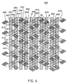
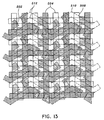
- Trenches 202 are shaped in the form of a parallelogram. This is to maintain the substantially parallel alignment of trenches 202 with angled portions 208 of active areas 206.
- Wordlines 204 are oriented in a substantially parallel manner as before.
- the parallelogram shapes of trenches 202 permit increased memory cell density across memory chip 200.
- angled portions 208 form an angle B between wordlines 204. Angle B may be greater than 0 degrees to about 60 degrees.
- the angles of the parallelogram formed by trenches 202 will shift appropriately in accordance to the active region 206 orientation. Angled portions 208 of active areas 206 connect to portions 210 which are substantially perpendicular to wordlines 204.
- Portions 210 connect to trenches 202 (through the buried strap).
- a distance d 3 between a wordline 204 and trench 202 is greater than or equal to F, the minimum feature size in accordance with the invention.
- the average distance across portion 210 is greater than F.
- a distance d 4 between a wordline 204 and trench 202 is greater than F, the minimum feature size in accordance with the invention.
- the average distance across portion 210 is greater than F, and the distance between all points of trench 202 and wordline 204 is greater than F. This is achieved by maintaining cornered bends 220 of active areas 206 which force the distance of all points between trenches 202 and wordlines 204 in active areas 206 to be greater than F.
- trenches 202 are spaced apart by about F on sides opposite active areas 206.
- Bitline contacts 122 are shown in FIGS. 4 and 5.
- a channel region 207 below wordlines 204 is also increased by angled portions 208 thereby reducing short channel effects in access transistors.
- FIGS. 6 and 7 another embodiment of the present invention employs trenches 302 with bent or arcuate shaped sides 301, and straight sides 303 which are substantially parallel to angled portions 308 of active areas 306.
- a distance d 5 is maintained greater than F for all points of portions 310 between wordlines 304 and trenches 302.
- the trenches 302 having the shape shown in FIGS. 6 and 7 more distance is gained between wordline 304 and trenches 302 thereby permitting increased overlay margin (tolerance).
- a channel region 307 below wordlines 304 is also increased by angled portions 308 thereby reducing short channel effects in access transistors.
- trenches 302 are spaced apart by about F on sides opposite active areas 306. Bitline contacts 322 are also shown.
- FIG. 7 includes the advantages of corners 320 of portions 310 of active areas 306.
- trenches 402 may be angled to optimize or increase the trench area, i.e., to provide larger trenches.
- trenches 403 may slanted to provide a more efficient and larger layout area.
- wordlines 404 may be thicker to increase the area of the trench and provide a larger channel length of a transistor channel 406 below wordlines 404.
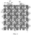
- wordlines 407 may be widened in appropriate places as shown in FIGS. 10 and 11.
- Wordlines 407 have a wiggle or "toothed" appearance to provide expanded portions 409 over channels 406 to increase channel length.
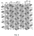
- trapezoids may be employed for trenches 502 along with angled portions 508 of active areas 506.
- Portions 510 may include corners 512 as described above.
- Wordlines are labeled as 504.
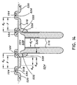
- FIG. 14 a cross-sectional view of the layout of FIG. 3 is shown.
- Storage nodes 516 are isolated from a doped well 524 by a dielectric collar 526. Shallow trench isolation 528 is provided over storage nodes 516 to electrically isolate the passing wordlines 104 formed above storage nodes 516.
- Diffusion regions 518 (portions 110 of active areas 106) of access transistors 514 are connected to storage node 516 by a node diffusion region 530 to a buried strap 532. Node diffusion 530 and buried strap 532 are connected by outdiffusing dopants which mix to create a conductive region (node region 530) therebetween.
- the distance between wordlines 104 and buried strap 532 is greater than F.
- the dopant outdiffusion from buried strap 532 cannot outdiffuse far enough to interact with a channel 534 below a gate 536 (wordline 104) thereby preventing short channel effects in access transistor 514.
- wordline 10 a gate 536
- the present invention advantageously leaves margin between wordline 104 and diffusion regions 518 and 520 and buried strap 532 outdiffusion. d 1 may be maintained at F.
- channel 534 still has margin due to the fact that the distance d 2 is increased according to the invention.
- d 2 can be larger as described in accordance with the various embodiments and combinations thereof
Landscapes
- Engineering & Computer Science (AREA)
- Microelectronics & Electronic Packaging (AREA)
- Computer Hardware Design (AREA)
- Semiconductor Memories (AREA)
Applications Claiming Priority (2)
| Application Number | Priority Date | Filing Date | Title |
|---|---|---|---|
| US09/272,215 US6211544B1 (en) | 1999-03-18 | 1999-03-18 | Memory cell layout for reduced interaction between storage nodes and transistors |
| US272215 | 2008-11-17 |
Publications (2)
| Publication Number | Publication Date |
|---|---|
| EP1037280A2 true EP1037280A2 (fr) | 2000-09-20 |
| EP1037280A3 EP1037280A3 (fr) | 2001-04-11 |
Family
ID=23038881
Family Applications (1)
| Application Number | Title | Priority Date | Filing Date |
|---|---|---|---|
| EP00103617A Withdrawn EP1037280A3 (fr) | 1999-03-18 | 2000-02-21 | Configuration de cellules "mémoires" pour une intéraction réduite entre les noeuds de stockage et les transistors |
Country Status (6)
| Country | Link |
|---|---|
| US (1) | US6211544B1 (fr) |
| EP (1) | EP1037280A3 (fr) |
| JP (1) | JP2000269464A (fr) |
| KR (1) | KR100424820B1 (fr) |
| CN (1) | CN1153294C (fr) |
| TW (1) | TW448480B (fr) |
Cited By (2)
| Publication number | Priority date | Publication date | Assignee | Title |
|---|---|---|---|---|
| US7372095B2 (en) | 2003-02-28 | 2008-05-13 | Infineon Technologies Ag | Integrated semiconductor circuit comprising a transistor and a strip conductor |
| WO2014184299A1 (fr) * | 2013-05-16 | 2014-11-20 | Ps4 Luxco S.A.R.L. | Dispositif de mémoire à semi-conducteurs doté d'une disposition améliorée de zones actives/lignes de mots |
Families Citing this family (15)
| Publication number | Priority date | Publication date | Assignee | Title |
|---|---|---|---|---|
| DE19813169A1 (de) * | 1998-03-25 | 1999-10-07 | Siemens Ag | Halbleiterspeicher mit streifenförmiger Zellplatte |
| DE10027912A1 (de) * | 2000-05-31 | 2001-12-13 | Infineon Technologies Ag | Speicherzellenanordnung |
| US6727540B2 (en) * | 2002-08-23 | 2004-04-27 | International Business Machines Corporation | Structure and method of fabricating embedded DRAM having a vertical device array and a bordered bitline contact |
| KR100663402B1 (ko) * | 2004-01-20 | 2007-01-02 | 엘지전자 주식회사 | 휴대용 단말기에서의 전력라인 통신장치 |
| US20060151845A1 (en) * | 2005-01-07 | 2006-07-13 | Shrinivas Govindarajan | Method to control interfacial properties for capacitors using a metal flash layer |
| US7316962B2 (en) * | 2005-01-07 | 2008-01-08 | Infineon Technologies Ag | High dielectric constant materials |
| US20060151822A1 (en) * | 2005-01-07 | 2006-07-13 | Shrinivas Govindarajan | DRAM with high K dielectric storage capacitor and method of making the same |
| JP2007035957A (ja) * | 2005-07-27 | 2007-02-08 | Toshiba Corp | 半導体装置とその製造方法 |
| JP5694625B2 (ja) * | 2006-04-13 | 2015-04-01 | ピーエスフォー ルクスコ エスエイアールエルPS4 Luxco S.a.r.l. | 半導体記憶装置 |
| KR101353343B1 (ko) * | 2007-09-18 | 2014-01-17 | 삼성전자주식회사 | 활성 영역 상에서 비트라인 패턴의 일 측부로부터 서로다른 거리들로 각각 이격되는 스토리지 노드들을 가지는반도체 장치들 및 그 형성방법들 |
| JP2011134981A (ja) * | 2009-12-25 | 2011-07-07 | Sanyo Electric Co Ltd | 不揮発性半導体記憶装置及びその製造方法 |
| US10026740B1 (en) | 2017-10-30 | 2018-07-17 | Globalfoundries Inc. | DRAM structure with a single diffusion break |
| CN110707082B (zh) * | 2018-10-09 | 2022-04-12 | 联华电子股份有限公司 | 形成半导体装置布局的方法 |
| TWI811517B (zh) | 2020-01-16 | 2023-08-11 | 聯華電子股份有限公司 | 磁阻式隨機存取記憶體之佈局圖案 |
| CN116113237B (zh) | 2020-08-18 | 2024-11-15 | 长鑫存储技术有限公司 | 存储器及其制作方法 |
Citations (2)
| Publication number | Priority date | Publication date | Assignee | Title |
|---|---|---|---|---|
| US4859615A (en) * | 1985-09-19 | 1989-08-22 | Mitsubishi Denki Kabushiki Kaisha | Semiconductor memory cell capacitor and method for making the same |
| EP0858109A2 (fr) * | 1997-02-07 | 1998-08-12 | Nec Corporation | Dispositif semi-conducteur à mémoire et son procédé de fabrication |
Family Cites Families (12)
| Publication number | Priority date | Publication date | Assignee | Title |
|---|---|---|---|---|
| JPH01199465A (ja) * | 1988-02-04 | 1989-08-10 | Fujitsu Ltd | 半導体記憶装置 |
| JPH02106958A (ja) * | 1988-10-17 | 1990-04-19 | Hitachi Ltd | 半導体装置 |
| JPH0821690B2 (ja) * | 1990-03-19 | 1996-03-04 | 富士通株式会社 | 半導体記憶装置 |
| JPH04134857A (ja) * | 1990-09-27 | 1992-05-08 | Toshiba Corp | 半導体記憶装置 |
| JP3128834B2 (ja) * | 1991-01-28 | 2001-01-29 | 日本電気株式会社 | 半導体装置 |
| JPH04326572A (ja) * | 1991-04-25 | 1992-11-16 | Texas Instr Japan Ltd | トレンチ型半導体装置 |
| JPH04328860A (ja) * | 1991-04-30 | 1992-11-17 | Hitachi Ltd | 半導体集積回路装置及びその製造方法 |
| JP2819958B2 (ja) * | 1991-09-13 | 1998-11-05 | 日本電気株式会社 | 半導体記憶装置 |
| KR970001894B1 (en) * | 1991-09-13 | 1997-02-18 | Nippon Electric Kk | Semiconductor memory device |
| US5576566A (en) * | 1995-04-13 | 1996-11-19 | International Business Machines Corporation | Semiconductor trench capacitor cell having a buried strap |
| US5998821A (en) * | 1997-05-21 | 1999-12-07 | Kabushiki Kaisha Toshiba | Dynamic ram structure having a trench capacitor |
| TW393731B (en) * | 1997-12-01 | 2000-06-11 | Nanya Plastics Corp | DRAM sharing a bit line contact window with multi-memory cells and its manufacturing method |
-
1999
- 1999-03-18 US US09/272,215 patent/US6211544B1/en not_active Expired - Lifetime
-
2000
- 2000-02-21 EP EP00103617A patent/EP1037280A3/fr not_active Withdrawn
- 2000-03-08 TW TW089104144A patent/TW448480B/zh not_active IP Right Cessation
- 2000-03-17 KR KR10-2000-0013584A patent/KR100424820B1/ko not_active Expired - Fee Related
- 2000-03-17 JP JP2000077068A patent/JP2000269464A/ja not_active Withdrawn
- 2000-03-20 CN CNB001043641A patent/CN1153294C/zh not_active Expired - Fee Related
Patent Citations (2)
| Publication number | Priority date | Publication date | Assignee | Title |
|---|---|---|---|---|
| US4859615A (en) * | 1985-09-19 | 1989-08-22 | Mitsubishi Denki Kabushiki Kaisha | Semiconductor memory cell capacitor and method for making the same |
| EP0858109A2 (fr) * | 1997-02-07 | 1998-08-12 | Nec Corporation | Dispositif semi-conducteur à mémoire et son procédé de fabrication |
Cited By (2)
| Publication number | Priority date | Publication date | Assignee | Title |
|---|---|---|---|---|
| US7372095B2 (en) | 2003-02-28 | 2008-05-13 | Infineon Technologies Ag | Integrated semiconductor circuit comprising a transistor and a strip conductor |
| WO2014184299A1 (fr) * | 2013-05-16 | 2014-11-20 | Ps4 Luxco S.A.R.L. | Dispositif de mémoire à semi-conducteurs doté d'une disposition améliorée de zones actives/lignes de mots |
Also Published As
| Publication number | Publication date |
|---|---|
| TW448480B (en) | 2001-08-01 |
| EP1037280A3 (fr) | 2001-04-11 |
| US6211544B1 (en) | 2001-04-03 |
| CN1267914A (zh) | 2000-09-27 |
| KR20000062935A (ko) | 2000-10-25 |
| KR100424820B1 (ko) | 2004-03-27 |
| JP2000269464A (ja) | 2000-09-29 |
| CN1153294C (zh) | 2004-06-09 |
Similar Documents
| Publication | Publication Date | Title |
|---|---|---|
| US6211544B1 (en) | Memory cell layout for reduced interaction between storage nodes and transistors | |
| US6355954B1 (en) | Device with asymmetrical channel dopant profile | |
| US6906372B2 (en) | Semiconductor device with vertical transistor formed in a silicon-on-insulator substrate | |
| US5378906A (en) | Dynamic random access memory having improved layout | |
| US5014103A (en) | Dynamic random access memory having improved layout and method of arranging memory cell pattern of the dynamic random access memory | |
| KR100403066B1 (ko) | 반도체 메모리 셀 어레이 구조물 형성 방법 | |
| US6396096B1 (en) | Design layout for a dense memory cell structure | |
| US20070152263A1 (en) | Dynamic random access memory cell layout and fabrication method thereof | |
| US7183595B2 (en) | Ferroelectric memory | |
| WO2024060365A1 (fr) | Pilote de ligne de mots, et appareil de stockage | |
| US5838036A (en) | Semiconductor memory device capable of realizing a minimum memory cell area approximate to a theoretical value | |
| US6291846B1 (en) | DRAM semiconductor device including oblique area in active regions and its manufacture | |
| US6903414B2 (en) | Semiconductor memory having channel regions at sides of a trench | |
| US5671175A (en) | Capacitor over bitline DRAM cell | |
| JP3238066B2 (ja) | 半導体記憶装置およびその製造方法 | |
| US20050176193A1 (en) | Method of forming a gate of a semiconductor device | |
| US6781181B2 (en) | Layout of a folded bitline DRAM with a borderless bitline | |
| US5234853A (en) | Method of producing a high voltage MOS transistor | |
| KR940008222B1 (ko) | 고전압 mos 트랜지스터 및 그 제조방법과 고전압 mos 트랜지스터를 갖는 반도체 장치 및 그 제조방법 | |
| US7332390B2 (en) | Semiconductor memory device and fabrication thereof | |
| US4958212A (en) | Trench memory cell | |
| US5241205A (en) | Semiconductor memory device | |
| US6875653B2 (en) | DRAM cell structure with buried surrounding capacitor and process for manufacturing the same | |
| US6600195B1 (en) | Semiconductor device | |
| HK1031463A (en) | Memory cell layout for reduced interaction between storage nodes and transistors |
Legal Events
| Date | Code | Title | Description |
|---|---|---|---|
| PUAI | Public reference made under article 153(3) epc to a published international application that has entered the european phase |
Free format text: ORIGINAL CODE: 0009012 |
|
| AK | Designated contracting states |
Kind code of ref document: A2 Designated state(s): DE FR GB IE IT NL |
|
| AX | Request for extension of the european patent |
Free format text: AL;LT;LV;MK;RO;SI |
|
| PUAL | Search report despatched |
Free format text: ORIGINAL CODE: 0009013 |
|
| AK | Designated contracting states |
Kind code of ref document: A3 Designated state(s): AT BE CH CY DE DK ES FI FR GB GR IE IT LI LU MC NL PT SE |
|
| AX | Request for extension of the european patent |
Free format text: AL;LT;LV;MK;RO;SI |
|
| 17P | Request for examination filed |
Effective date: 20010707 |
|
| AKX | Designation fees paid |
Free format text: DE FR GB IE IT NL |
|
| 17Q | First examination report despatched |
Effective date: 20060915 |
|
| STAA | Information on the status of an ep patent application or granted ep patent |
Free format text: STATUS: THE APPLICATION IS DEEMED TO BE WITHDRAWN |
|
| 18D | Application deemed to be withdrawn |
Effective date: 20110830 |