EP1047261A2 - Bildpuffer mit mehreren Zugriffsmoden - Google Patents
Bildpuffer mit mehreren Zugriffsmoden Download PDFInfo
- Publication number
- EP1047261A2 EP1047261A2 EP00302469A EP00302469A EP1047261A2 EP 1047261 A2 EP1047261 A2 EP 1047261A2 EP 00302469 A EP00302469 A EP 00302469A EP 00302469 A EP00302469 A EP 00302469A EP 1047261 A2 EP1047261 A2 EP 1047261A2
- Authority
- EP
- European Patent Office
- Prior art keywords
- data
- memory
- image
- burst
- processor
- Prior art date
- Legal status (The legal status is an assumption and is not a legal conclusion. Google has not performed a legal analysis and makes no representation as to the accuracy of the status listed.)
- Granted
Links
Images


Classifications
-
- G—PHYSICS
- G06—COMPUTING OR CALCULATING; COUNTING
- G06T—IMAGE DATA PROCESSING OR GENERATION, IN GENERAL
- G06T1/00—General purpose image data processing
-
- H—ELECTRICITY
- H04—ELECTRIC COMMUNICATION TECHNIQUE
- H04N—PICTORIAL COMMUNICATION, e.g. TELEVISION
- H04N1/00—Scanning, transmission or reproduction of documents or the like, e.g. facsimile transmission; Details thereof
- H04N1/21—Intermediate information storage
- H04N1/2104—Intermediate information storage for one or a few pictures
- H04N1/2112—Intermediate information storage for one or a few pictures using still video cameras
- H04N1/2137—Intermediate information storage for one or a few pictures using still video cameras with temporary storage before final recording, e.g. in a frame buffer
-
- G—PHYSICS
- G06—COMPUTING OR CALCULATING; COUNTING
- G06T—IMAGE DATA PROCESSING OR GENERATION, IN GENERAL
- G06T1/00—General purpose image data processing
- G06T1/60—Memory management
-
- H—ELECTRICITY
- H04—ELECTRIC COMMUNICATION TECHNIQUE
- H04N—PICTORIAL COMMUNICATION, e.g. TELEVISION
- H04N1/00—Scanning, transmission or reproduction of documents or the like, e.g. facsimile transmission; Details thereof
- H04N1/21—Intermediate information storage
- H04N1/2104—Intermediate information storage for one or a few pictures
- H04N1/2112—Intermediate information storage for one or a few pictures using still video cameras
Definitions
- the invention relates to image processing, and more particularly to a method and system for allowing a data processor to efficiently access image data from a memory in multiple formats.
- an image sensor within an image gathering device such as a charge-coupled device (CCD) or a CMOS sensor, converts a picture frame of image light information to electronic analog signals.
- the resultant analog image signals are converted by an analog-to-digital converter (ADC) to digital image data.
- ADC analog-to-digital converter
- the digital image data is then transferred to a memory storage device.
- Burst access memories such as synchronous dynamic random access memory (SDRAM) or conventional burst DRAMs are popular in camera designs for their ability to output large amounts of data quickly.
- a data processor such as a digital signal processor (digital signal processor) typically accesses data a bit at a time by referring to a specific bit address in the DRAM.
- a burst access memory is designed to output multiple data bits based on a single address reference. Therefore, in conventional imaging systems that use a DSP and a burst access memory, the data burst is not fully used.
- the DSP addresses the memory for each bit of data it requires.
- it is particularly advantageous to access stored data block by block which a burst access memory is well suited for, rather than line by line or bit by bit.
- DSPs are not particularly suited for retrieving block data from memory, however. For example, in performing a seven-tap filtering function, the processor will request seven bursts of data from the memory and the read/write overhead will be 21 clock cycles, assuming once again that three clock cycles are necessary for each burst.
- the brightness of the photographed image is controlled by means of a diaphragm mechanism by driving the lens control device in accordance with brightness data of the photographed object detected by an auto exposure sensor and an auto-exposure calculating device.
- color adjustment (white balance adjustment) of the photographed image input by the charge-coupled device is executed by obtaining a color temperature of the photographed object in accordance with color data of the object detected by a white balance sensor and a white balance calculating device.
- the present invention provides an image buffer which can execute auto exposure and white balance by sub-sampling (down-sampling) the photographed image data stored in the memory and then transferring the sampled image data to the processor for exposure calculation and white balance calculation when the photographed image data are retrieved either in line access mode or in block access mode in response to a request from the processor.
- the sampling rate can be controlled by the processor in a programmable manner and the auto exposure and auto white balance of the photographed image data can be executed efficiently while still providing satisfactory results.
- One embodiment of the invention is an image processing system comprising a memory capable of storing a picture frame of image data and outputting the data in a format comprising one or more bursts of data, a data processor capable of processing at a given time an amount of data less than the one or more bursts of data and a data buffer coupled between the memory and the data processor.
- the data buffer has a size sufficient to store the one or more bursts of data and capable of outputting an amount of data within the processing capability of the data processor.
- the format can comprise a block of data, a line of data, or data sampled from spatially diverse locations within the picture frame of data.
- Another embodiment of the invention is an image processing system comprising a burst memory, a data processor and a data buffer coupled between the burst memory and the data processor.
- the data buffer comprises a block memory coupled to the burst memory and to the data processor and an access controller coupled to the block memory, to the data processor and to the burst memory.
- the access controller transfers data from the burst memory to the block memory in a format specified to the access controller by the data processor.
- the access controller also transfers the formatted data from the block memory to the data processor.
- the format can comprise a block of data, a line of data, or data sampled from spatially diverse locations within the picture frame of data.
- a method of processing image data in a camera comprises the steps of storing the image data in a memory, selecting a portion of the image data in a format determined by a data processor coupled to the memory, storing the formatted data in a second memory and transferring the formatted data to the data processor.
- One advantage of the invention is that it provides an efficient interface between a processor and a memory like a burst access DRAM by, for example, increasing the processing bandwidth of the processor by reducing the overhead for data access.
- Another advantage of the invention is that it allows for sampling of data within an image that can be used in image enhancement calculations performed by the data processor.
- One embodiment of the invention provides a highly efficient block type single port image buffer as an interface between a data processor (e.g. a digital signal processor) and an SDRAM controller such that the image data within the SDRAM can be retrieved in a block access mode, a line access mode or a sub-sampling mode in response to the control signals from the digital signal processor.
- the image buffer comprises a block buffer, an access controller and a switch wherein the block buffer is a shared memory of the data processor and the SDRAM controller.
- the access controller can be set in a block access mode, a line access mode or a sub-sampling mode by the data processor via the internal control bus therebetween.
- the selection of the block access mode, line access mode and sub-sampling mode is based on the type of data to be processed by the data processor.
- the block access mode is suitable for flexibly processing the image taken by the CCD sensors
- the line access mode is suitable for storing normal format data, such as operating system instructions, voice data received from a microphone built into the camera, or an external voice source.
- the sub-sampling mode is selected, for example, when the focusing, exposure control, and white balance of the photographed image data are to be performed.
- the functions of focusing, exposure control, and white balance of the photographed image data are done by computing image statistics based on image data in the data processor.
- the computed values are then used by a program implemented in the data processor that decides how to adjust the focus motor, aperture, auto gain control, and auto white balance control.
- the switch is configured to selectively connect the block buffer either to the data processor or to the SDRAM controller in response to a control signal from the access controller.
- the block buffer is a shared memory of the data processor and the SDRAM controller.
- the data processor first sends some basic information concerning the data to be processed to the access controller.
- the data to be processed may be block(s), line(s), or interleaved bursts within a picture frame of data.
- the access controller then generates the address of the data to be processed and provides it to the SDRAM controller based on the received basic information.
- the data to be processed by the processor will be temporarily moved by the SDRAM controller to the block buffer in a block access mode, a line access mode or a sub-sampling mode.
- the data processor halts the currently processing job in order to receive the data from the block buffer in response to an interrupt signal from the image buffer.
- an access controller and a block buffer within the image buffer access the image data to be processed by the data processor from the SDRAM in different access modes.
- the image buffer can access the SDRAM in a block access mode in which image data within a picture frame is accessed with an address offset being equal to one line width.
- the image buffer can access the SDRAM in a line access mode in which contiguous data within a picture frame are accessed with the address offset being equal to one burst size of data which can be accessed from the SDRAM per clock cycle.
- the size of a block or the number of bursts for one access operation can be set by the data processor.
- the image buffer can perform sub-sampling of the image data to be processed by the data processor by setting the address offset to be the sub-sampling interval (e.g. an integral multiple of the burst size of data that can be accessed from the SDRAM per clock cycle).
- the different address offsets can be set by the data processor and are sent to the access controller within the image buffer to achieve the different access modes.
- embodiments of the invention provide a data interface between the data processor and the memory for processing data more efficiently.
- the invention is illustrated and explained hereinbelow with reference to a digital still camera, but one skilled in the art will appreciate that the scope of the invention is not limited thereto.
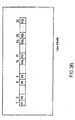
- Fig. 1 depicts a simplified schematic block diagram of a digital signal processing system.
- Reference numeral 1 denotes a photographing lens optical system receiving the image light of a photographed object.
- CCD charge-coupled device
- An A/D converter 3 transforms the analog image signal into digital image data.
- a CCD controller 4 then transfers the digital image data via an SDRAM controller 5 to a semiconductor memory such as a synchronous dynamic random access memory (SDRAM) 6 for temporary storage.
- SDRAM synchronous dynamic random access memory
- the image data from the SDRAM 6 is further processed by an encoder controller 9 and an NTSC/PAL encoder 10.
- this embodiment of the invention provides an image buffer 8 as an image data interface between the SDRAM controller 5 and the digital signal processor 7.
- the image buffer 8 comprises a block buffer 81, which is a shared memory of the digital signal processor 7 and the SDRAM controller 5, an access controller 82 and a switch 83.
- the block buffer 81 has a size of 16x22 pixels, which is suitable enough for a frame of image data in JPEG format (the size for JPEG image data is 8x8 bits).
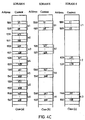
- the access controller 82 can be set in a block access mode (Fig. 3A), a line access mode (Fig. 3B) or a sub-sampling mode (Fig. 3C) by the digital signal processor 7 via the internal control bus 84 therebetween.
- the switch 83 is configured to selectively connect the block buffer 81 either to the digital signal processor 7 or to the SDRAM controller 5 in response to a control signal from the access controller 82.
- the switch may be implemented as a multiplexer or similar circuit.
- data at a certain location within the SDRAM 6 to be processed by the digital signal processor 7 will be temporarily moved through image bus 85 and bus 86 to the block buffer 81 in a block access mode, a line access mode or a sub-sampling mode in response to a request from the digital signal processor 7 via bus 84.
- the data Once the data is in block buffer 81, it can be accessed by the digital signal processor 7.
- the block access mode, line access mode or sub-sampling mode is selectable based on the type of data within the SDRAM 6 that the digital signal processor 7 is to access.
- the block access mode is especially suitable for the digital signal processor 7 to process any portion(s) of block type image data located in a picture frame of data captured by the CCD 2.
- the line access mode can be used for the digital signal processor 7 to process any portion(s) of strip type image data located in a picture frame of data, or when line mode is the normal data storage format, such as with voice data received from a microphone (not shown) built into the camera or from external voice equipment.
- the digital signal processor 7 can also retrieve the image data from the SDRAM 6 in a sub-sampling mode (Fig. 3C) by sending a sub-sampling rate to the access controller 82 via the bus 84.
- the digital signal processor 7 can also retrieve the image data from the SDRAM 6 in a sub-sampling, block access mode or a sub-sampling, line access mode by setting the sub-sampling rate, the block starting address, and the offset of the image data in the access controller 82.
- the access controller 82 comprises a termination signal generator 90 and an address generator 91.
- the termination signal generator 90 configured to generate an enabling signal indicating that the burst access of image data within the SDRAM 6 is finished, comprises a burst counter 901, a burst number register 902, and a comparator 903.
- the burst counter 901 is an up counter, which has an integral increment counter at the output thereof per clock cycle synchronous with the SDRAM controller 5.
- the burst number register 902 is programmed by the digital signal processor 7 to store the burst number of the image data to be processed by the digital signal processor 7.
- the digital signal processor 7 retrieves image data from the SDRAM 6 via the image buffer 8
- the digital signal processor 7 sends a control signal through bus 84 to the access controller 82 within the image buffer 8.
- the access controller 82 then accordingly controls the switch 83 via control line 88 to receive the address information of the image data to be retrieved via bus 89.
- the address information of the image data to be retrieved such as the burst number, or whether the retrieved data will be in block mode, line mode or sub-sampling mode having a certain sub-sampling rate, is then fed into the termination signal generator 90 and address generator 91.
- the comparator 903 When the burst number set by the digital signal processor 7 within the burst number register 902 equals the progressively counting value output by the burst counter 901, the comparator 903 will generate an enabling signal to the SDRAM controller 5, indicating that the burst access of the image data within the SDRAM 6 is finished.
- the termination signal generator 90 can be implemented with a down counter in which the starting count value is equal to the burst number set by the digital signal processor 7. When down-counting to zero, the down counter will send an enabling signal to the SDRAM controller 5, indicating termination of the block access of the image data.
- the address generator 91 configured to generate the starting address of each burst of image data located in different memory locations, comprises a starting address register 911 for storing the starting address of the first burst of the image data being retrieved by the digital signal processor 7, an offset register 912 programmed by the digital signal processor 7 for storing the jumping distance between two discontinuous bursts of image data, and an address refreshing register 913 for storing the starting address of the burst of image data being currently retrieved and corresponding to the burst number generated by the burst counter 901.
- the address generator 91 After receiving the address information regarding the image data to be retrieved by the digital signal processor 7, the address generator 91 generates various addresses of memory locations of the image data to be retrieved within a picture frame of data.
- the address generator 91 can also be modified by utilizing a single register for storing both the starting address value stored in register 911 and the offset address value stored in register 913.
- a circuit for iteratively summing one variable value with one fixed value is suitable for replacing the address refreshing register 913 and the offset register 912.
- the access controller 82 is operated in a block access mode if the offset register 912 is set to have a value equal to a line width of a picture frame (e.g. 640x480 pixels) of data.
- this block of image data (P11...P18, P21...P28, and P31...P38) can be located in three different memory locations ranging from addresses denoted 100 to 107, 740 to 747, and 940 to 947, for example (see Fig. 4A).
- the data my be accessed in three separate bursts of image data separated from one another as shown in Fig. 4A.
- the burst number register 902 and the starting address register 911 are programmed by the digital signal processor 7 to have values of 3 and 100, respectively, and the offset register 912 is programmed by the digital signal processor 7 to have a value equal to a line width of a picture frame, for example 640 pixels (which corresponds to 640 memory address differences if one pixel corresponds to one word).
- the switch 83 is then prompted by the access controller 82 to connect to SDRAM controller 5 through the bus 85.
- the address refreshing register 913 first loads the starting address value (100) stored in the starting address register 911 to the SDRAM controller 5 for locating the first burst of image data via the switch 83 and the bus 85.
- the burst counter 901 counts one.
- the starting address value is fed via a feedback loop 914 to an adder 915 for addition with the offset value (640) from the offset register 912.
- the sum (740) of the starting address value and the offset value is sent to the address refreshing register 913 and then transferred to the SDRAM controller 5 for locating the second burst of image data via the switch 83 and the bus 85.
- the burst counter 901 up-counts to two.
- the address value in the address refreshing register 913 is iteratively summed with the offset value in the offset register 912 until the burst counter 901 up-counts to the burst number (which is 3 in this case) stored in the burst number register 902.
- the access controller 82 prompts the switch 83 to interconnect the block buffer 81 and the digital signal processor 7 through bus 89 and bus 86, thus allowing the block buffer 81 to act as an internal memory buffer of the digital signal processor 7.
- the access controller 82 then sends an interrupt via the line 87 to the digital signal processor 7 to interrupt the current processing of the digital signal processor 7 and inform the digital signal processor 7 to sequentially access the image data (P11...P18, P21...P28, and P31...P38) within the block buffer 81.
- the digital signal processor 7 In the case of retrieving a block of image data within a picture frame of data, unlike the conventional digital signal processing architecture that accesses the bursts of image data separately located in the SDRAM 6 for plural clock cycles including three clock cycles, for initialization for accessing each burst of data, the digital signal processor 7 only needs to set in the image buffer 81 the burst size and the starting address of the image data to be retrieved within a single clock cycle. The digital signal processor 7 then executes other processing routines, and finally receives the retrieved image data, thereby significantly reducing processing time of the digital signal processor 7 on retrieving a block of image data within a picture frame of data.
- the digital signal processor 7 can therefore access the image data in a block access mode, which corresponds to several image blocks within a picture frame, whether the several blocks are adjacent to one another or not. These blocks of image data can be stored together in the block buffer 81 as long as the block buffer 81 is large enough, or can be stored sequentially in the block buffer 81 within several clock cycles.
- the image buffer 8 undertakes the time-consuming burden of accessing block(s) of image data, thus significantly reducing the read/write overhead of the digital signal processor 7 with increasing block size.
- the access controller 82 is operated in a line access mode when the offset register 912 is set to have the size of a burst which is the minimum unit of data that can be accessed from the SDRAM 6 at a time. As shown in Fig.
- this line of image data (P1, P2...P8, P9...P16, P17...P24, and P25...P32) is located in four adjacent memory locations ranging from addresses denoted 1000 to 1007, 1008 to 1015, 1016 to 1023, and 1024 to 1031 in Fig. 4B, thus forming four adjacent bursts of image data.
- the burst number register 902 and the starting address register 911 are programmed by the digital signal processor 7 through the bus 84 to have a value of 4 and 1000, respectively, and the offset register 912 is programmed by the digital signal processor 7 to have a value of the burst size of a picture frame (which is for example 8 memory locations in this case).
- the switch 83 is then prompted by the access controller 82 to connect to SDRAM controller 5 through the bus 85.
- the line access mode referring to Fig.
- the address refreshing register 913 first loads via bus 85 the starting address value stored in the starting address register 911 to the SDRAM controller 5 for locating the first burst of image data.
- the burst counter 901 counts one.
- the starting address value (1000) is fed via a feedback loop 914 to an adder 915 for addition with the offset value (8) from the offset register 912.
- the sum (1008) of the starting address value and the offset value is sent to the address refreshing register 913 and then transferred via bus 85 to the SDRAM controller 5 for locating the second burst of image data.
- the burst counter 901 up-counts to two.
- the address value in the address refreshing register 913 is iteratively summed with the offset value in the offset register 912 until the burst counter 901 up-counts to the burst number (which is 4 in this case) stored in the burst number register 902.
- the access controller 82 prompts the switch 83 to interconnect the block buffer 81 and the digital signal processor 7 through bus 86 and bus 89, thus allowing the block buffer 81 to be used as an internal memory buffer of the digital signal processor 7.
- the access controller 82 then sends an interrupt via the line 87 to the digital signal processor 7 to interrupt the current processing of the digital signal processor 7 and prompt the digital signal processor 7 to access image data within the block buffer 81.
- the digital signal processor 7 In the case of retrieving a line of image data within a picture frame of data (in which the offset value is given as the burst size of data that can be accessed from the SDRAM per clock cycle), the digital signal processor 7 only has to set the burst number and the starting address of the image data to be retrieved. This significantly reduces processing time of the digital signal processor 7 upon retrieving a line of image data within a picture frame of data.
- the digital signal processor 7 can therefore access the image data in a line access mode, which can correspond to several image lines within a picture frame of data whether those several lines are adjacent to one another or not.
- the aspects of the invention mentioned above can apply to the analysis of image parameters such as chroma, brightness, and so on.
- the access controller 82 can be operated in a sub-sampling mode to capture data from spatially diverse locations within a picture frame of data when the offset value stored in the offset register 912 is the sub-sampling distance between two adjacent sampled bursts.
- this spatially diverse image data (a1, a2...a7; b1, b2, b3; c1, c2) within a picture frame for cases (a)-(c) are located in several separate memory locations as shown in Fig. 4C.
- the burst number register 902 and the starting address register 911 are programmed by the digital signal processor 7 to have a value of 7 and 1500, respectively, and the offset register 912 is programmed by the digital signal processor 7 to have a value equal to the sub-sampling distance of a picture frame of data (for example, 10 pixels for case (a), 20 pixels for case (b), and 30 pixels for case (c)).
- the address refreshing register 913 first loads the starting address value stored in the starting address register 911 to the SDRAM controller 5 for locating the first burst of image data.
- the burst counter 901 counts one.
- the starting address value (1500) is fed via the feedback loop 914 to the adder 915 for addition with the offset value (10 for case (a), 20 for case (b), and 30 for case (c) from the offset register 912).
- the sum (1510, 1520 or 1530) of the starting address value and the offset value is sent to the address refreshing register 913 and then transferred to the SDRAM controller 5 for locating the second burst of image data.
- the burst counter 901 up-counts to two. In this way, the address value in the address refreshing register 913 is iteratively summed with the offset value in the offset register 912 until the burst counter 901 up-counts to the burst number (which is 7 in this case) stored in the burst number register 902.
- the access controller 82 prompts the switch 83 to interconnect the block buffer 81 and the digital signal processor 7, thus allowing the block buffer 81 to be used as an internal memory buffer of the digital signal processor 7.
- Access controller 82 then sends an interrupt to the digital signal processor 7 to interrupt the current processing of the digital signal processor 7 and prompts the digital signal processor 7 to access the sub-sampled image data within the block buffer 81.
- the digital signal processor 7 can process the sub-sampled image data to effectively obtain the color attributes of the picture frame such as chroma, brightness, and so on.
- the digital signal processor 7 In the case of retrieving in a sub-sampled image data within a picture frame of data, the digital signal processor 7 only has to set the burst number, the sub-sampling rate and the starting address of the sub-sampled image data to be retrieved.
- the digital signal processor 7 can therefore access the image data in a sub-sampling mode, which corresponds to several image bursts within a picture frame of data whether these several bursts are adjacent to one another or not.
- This function can be used to provide sampled data for the calculation of parameters such as white balance, exposure (AE) and focus without the need for sensors dedicated to those purposes. The results of these calculations can then be used in the standard manner to adjust the image quality of the system.
- the digital signal processor 7 can also retrieve the image data from the SDRAM 6 in a sub-sampled, block access mode or a sub-sampled, line access mode by providing the sub-sampling rate, the block starting address, the offset of the image data to the access controller 82.
- the digital signal processor 7 can process a flexible amount of the image data within a picture frame of data by merely setting the parameters regarding the processing mode and the locations of the image data in the image buffer 8, thus significantly reducing the read/write overhead and interrupt latency of the digital signal processor 7.
Landscapes
- Engineering & Computer Science (AREA)
- Multimedia (AREA)
- Signal Processing (AREA)
- Physics & Mathematics (AREA)
- General Physics & Mathematics (AREA)
- Theoretical Computer Science (AREA)
- Image Input (AREA)
- Studio Devices (AREA)
- Information Transfer Systems (AREA)
- Processing Of Color Television Signals (AREA)
Applications Claiming Priority (2)
| Application Number | Priority Date | Filing Date | Title |
|---|---|---|---|
| US12658499P | 1999-03-26 | 1999-03-26 | |
| US126584P | 1999-03-26 |
Publications (3)
| Publication Number | Publication Date |
|---|---|
| EP1047261A2 true EP1047261A2 (de) | 2000-10-25 |
| EP1047261A3 EP1047261A3 (de) | 2001-12-19 |
| EP1047261B1 EP1047261B1 (de) | 2006-06-28 |
Family
ID=22425635
Family Applications (1)
| Application Number | Title | Priority Date | Filing Date |
|---|---|---|---|
| EP00302469A Expired - Lifetime EP1047261B1 (de) | 1999-03-26 | 2000-03-27 | Bildpuffer mit mehreren Zugriffsmoden |
Country Status (6)
| Country | Link |
|---|---|
| EP (1) | EP1047261B1 (de) |
| JP (1) | JP2000316121A (de) |
| KR (1) | KR20010020682A (de) |
| AT (1) | ATE332059T1 (de) |
| DE (1) | DE60029046T2 (de) |
| TW (1) | TW529300B (de) |
Cited By (1)
| Publication number | Priority date | Publication date | Assignee | Title |
|---|---|---|---|---|
| EP2159750A1 (de) * | 2008-08-29 | 2010-03-03 | NEC Electronics Corporation | Vorrichtung und Verfahren zur Verarbeitung von Bilddaten |
Families Citing this family (4)
| Publication number | Priority date | Publication date | Assignee | Title |
|---|---|---|---|---|
| KR100612414B1 (ko) * | 2003-04-28 | 2006-08-16 | 삼성전자주식회사 | 영상 데이터 처리 시스템 및 영상 데이터 독출/기입 방법 |
| JP4978818B2 (ja) * | 2008-06-10 | 2012-07-18 | 国立大学法人東北大学 | 固体撮像素子及びその駆動方法 |
| CN103475819B (zh) * | 2013-09-04 | 2017-01-18 | 青岛海信网络科技股份有限公司 | 超高清智能摄像机及其图像数据拼接方法 |
| CN103517066A (zh) * | 2013-09-24 | 2014-01-15 | 北京环境特性研究所 | 基于SoC的高清嵌入式视频编解码系统 |
Family Cites Families (6)
| Publication number | Priority date | Publication date | Assignee | Title |
|---|---|---|---|---|
| JPH02274158A (ja) * | 1989-04-17 | 1990-11-08 | Omron Corp | イメージ・スキャナ |
| US5239387A (en) * | 1989-11-30 | 1993-08-24 | Hewlett-Packard Company | Buffering control for accommodating variable data exchange rates |
| US5164831A (en) * | 1990-03-15 | 1992-11-17 | Eastman Kodak Company | Electronic still camera providing multi-format storage of full and reduced resolution images |
| DE69322316T2 (de) * | 1992-06-22 | 1999-04-29 | Fujitsu Ltd., Kawasaki, Kanagawa | Verfahren und Vorrichtung zum Lesen von Bildern eines Bildabtasters |
| JP2817107B2 (ja) * | 1992-12-28 | 1998-10-27 | キヤノン株式会社 | 画像入力装置 |
| JP3626514B2 (ja) * | 1994-01-21 | 2005-03-09 | 株式会社ルネサステクノロジ | 画像処理回路 |
-
2000
- 2000-03-24 JP JP2000083182A patent/JP2000316121A/ja active Pending
- 2000-03-25 KR KR1020000015307A patent/KR20010020682A/ko not_active Withdrawn
- 2000-03-27 DE DE60029046T patent/DE60029046T2/de not_active Expired - Lifetime
- 2000-03-27 AT AT00302469T patent/ATE332059T1/de not_active IP Right Cessation
- 2000-03-27 EP EP00302469A patent/EP1047261B1/de not_active Expired - Lifetime
- 2000-04-06 TW TW089105486A patent/TW529300B/zh not_active IP Right Cessation
Cited By (1)
| Publication number | Priority date | Publication date | Assignee | Title |
|---|---|---|---|---|
| EP2159750A1 (de) * | 2008-08-29 | 2010-03-03 | NEC Electronics Corporation | Vorrichtung und Verfahren zur Verarbeitung von Bilddaten |
Also Published As
| Publication number | Publication date |
|---|---|
| EP1047261B1 (de) | 2006-06-28 |
| EP1047261A3 (de) | 2001-12-19 |
| DE60029046D1 (de) | 2006-08-10 |
| TW529300B (en) | 2003-04-21 |
| DE60029046T2 (de) | 2006-11-30 |
| JP2000316121A (ja) | 2000-11-14 |
| KR20010020682A (ko) | 2001-03-15 |
| ATE332059T1 (de) | 2006-07-15 |
Similar Documents
| Publication | Publication Date | Title |
|---|---|---|
| JP4131052B2 (ja) | 撮像装置 | |
| US5493335A (en) | Single sensor color camera with user selectable image record size | |
| US20050078197A1 (en) | System and method for capturing image data | |
| JP4253881B2 (ja) | 撮像装置 | |
| CN101753820B (zh) | 信息处理装置、缓冲器控制方法和计算机程序 | |
| US6750909B1 (en) | Image buffer between burst memory and data processor with multiple access modes set by the data processor | |
| JP2000092375A (ja) | 信号処理装置及びその制御方法 | |
| EP1047261B1 (de) | Bildpuffer mit mehreren Zugriffsmoden | |
| CN111093006B (zh) | 摄像装置、信息处理装置、补偿量设定方法 | |
| JP2000224604A (ja) | 画像処理装置 | |
| JP4328906B2 (ja) | バス制御方法及び装置並びにデジタルカメラ | |
| US20050168623A1 (en) | Digital image production method and apparatus | |
| JP3696895B2 (ja) | ビデオカメラ及び映像信号処理方法 | |
| JP4284458B2 (ja) | デジタルカメラ | |
| US20070196100A1 (en) | Lens unit and digital camera | |
| JP4158245B2 (ja) | 信号処理装置 | |
| JPH08140025A (ja) | デジタルスチルカメラ | |
| JP4264602B2 (ja) | 画像処理装置 | |
| US20050078194A1 (en) | System and method for capturing image data | |
| JP4282202B2 (ja) | 電子カメラ | |
| WO2021152974A1 (ja) | 撮像素子、撮像装置、撮像素子の作動方法、及びプログラム | |
| JPH1175106A (ja) | 静止画カメラ | |
| JPH07131748A (ja) | 電子スチルビデオカメラ | |
| JP2009147885A (ja) | 撮像装置及び撮像方法 | |
| JPH11313230A (ja) | カメラ及び画像処理方法並びに記憶媒体 |
Legal Events
| Date | Code | Title | Description |
|---|---|---|---|
| PUAI | Public reference made under article 153(3) epc to a published international application that has entered the european phase |
Free format text: ORIGINAL CODE: 0009012 |
|
| AK | Designated contracting states |
Kind code of ref document: A2 Designated state(s): AT BE CH CY DE DK ES FI FR GB GR IE IT LI LU MC NL PT SE |
|
| AX | Request for extension of the european patent |
Free format text: AL;LT;LV;MK;RO;SI |
|
| PUAL | Search report despatched |
Free format text: ORIGINAL CODE: 0009013 |
|
| AK | Designated contracting states |
Kind code of ref document: A3 Designated state(s): AT BE CH CY DE DK ES FI FR GB GR IE IT LI LU MC NL PT SE |
|
| AX | Request for extension of the european patent |
Free format text: AL;LT;LV;MK;RO;SI |
|
| RIC1 | Information provided on ipc code assigned before grant |
Free format text: 7H 04N 1/21 A, 7G 06T 1/60 B |
|
| 17P | Request for examination filed |
Effective date: 20020521 |
|
| AKX | Designation fees paid |
Free format text: DE FR GB IT NL |
|
| RBV | Designated contracting states (corrected) |
Designated state(s): AT BE CH CY DE DK ES FI FR GB GR IE IT LI LU MC NL PT SE |
|
| 17Q | First examination report despatched |
Effective date: 20040304 |
|
| GRAP | Despatch of communication of intention to grant a patent |
Free format text: ORIGINAL CODE: EPIDOSNIGR1 |
|
| GRAS | Grant fee paid |
Free format text: ORIGINAL CODE: EPIDOSNIGR3 |
|
| GRAA | (expected) grant |
Free format text: ORIGINAL CODE: 0009210 |
|
| AK | Designated contracting states |
Kind code of ref document: B1 Designated state(s): AT BE CH CY DE DK ES FI FR GB GR IE IT LI LU MC NL PT SE |
|
| PG25 | Lapsed in a contracting state [announced via postgrant information from national office to epo] |
Ref country code: CH Free format text: LAPSE BECAUSE OF FAILURE TO SUBMIT A TRANSLATION OF THE DESCRIPTION OR TO PAY THE FEE WITHIN THE PRESCRIBED TIME-LIMIT Effective date: 20060628 Ref country code: IT Free format text: LAPSE BECAUSE OF FAILURE TO SUBMIT A TRANSLATION OF THE DESCRIPTION OR TO PAY THE FEE WITHIN THE PRE;WARNING: LAPSES OF ITALIAN PATENTS WITH EFFECTIVE DATE BEFORE 2007 MAY HAVE OCCURRED AT ANY TIME BEFORE 2007. THE CORRECT EFFECTIVE DATE MAY BE DIFFERENT FROM THE ONE RECORDED.SCRIBED TIME-LIMIT Effective date: 20060628 Ref country code: LI Free format text: LAPSE BECAUSE OF FAILURE TO SUBMIT A TRANSLATION OF THE DESCRIPTION OR TO PAY THE FEE WITHIN THE PRESCRIBED TIME-LIMIT Effective date: 20060628 Ref country code: BE Free format text: LAPSE BECAUSE OF FAILURE TO SUBMIT A TRANSLATION OF THE DESCRIPTION OR TO PAY THE FEE WITHIN THE PRESCRIBED TIME-LIMIT Effective date: 20060628 Ref country code: AT Free format text: LAPSE BECAUSE OF FAILURE TO SUBMIT A TRANSLATION OF THE DESCRIPTION OR TO PAY THE FEE WITHIN THE PRESCRIBED TIME-LIMIT Effective date: 20060628 Ref country code: FI Free format text: LAPSE BECAUSE OF FAILURE TO SUBMIT A TRANSLATION OF THE DESCRIPTION OR TO PAY THE FEE WITHIN THE PRESCRIBED TIME-LIMIT Effective date: 20060628 Ref country code: NL Free format text: LAPSE BECAUSE OF FAILURE TO SUBMIT A TRANSLATION OF THE DESCRIPTION OR TO PAY THE FEE WITHIN THE PRESCRIBED TIME-LIMIT Effective date: 20060628 |
|
| REG | Reference to a national code |
Ref country code: GB Ref legal event code: FG4D |
|
| REG | Reference to a national code |
Ref country code: CH Ref legal event code: EP |
|
| REG | Reference to a national code |
Ref country code: IE Ref legal event code: FG4D |
|
| REF | Corresponds to: |
Ref document number: 60029046 Country of ref document: DE Date of ref document: 20060810 Kind code of ref document: P |
|
| PG25 | Lapsed in a contracting state [announced via postgrant information from national office to epo] |
Ref country code: DK Free format text: LAPSE BECAUSE OF FAILURE TO SUBMIT A TRANSLATION OF THE DESCRIPTION OR TO PAY THE FEE WITHIN THE PRESCRIBED TIME-LIMIT Effective date: 20060928 Ref country code: SE Free format text: LAPSE BECAUSE OF FAILURE TO SUBMIT A TRANSLATION OF THE DESCRIPTION OR TO PAY THE FEE WITHIN THE PRESCRIBED TIME-LIMIT Effective date: 20060928 |
|
| PG25 | Lapsed in a contracting state [announced via postgrant information from national office to epo] |
Ref country code: ES Free format text: LAPSE BECAUSE OF FAILURE TO SUBMIT A TRANSLATION OF THE DESCRIPTION OR TO PAY THE FEE WITHIN THE PRESCRIBED TIME-LIMIT Effective date: 20061009 |
|
| PG25 | Lapsed in a contracting state [announced via postgrant information from national office to epo] |
Ref country code: PT Free format text: LAPSE BECAUSE OF FAILURE TO SUBMIT A TRANSLATION OF THE DESCRIPTION OR TO PAY THE FEE WITHIN THE PRESCRIBED TIME-LIMIT Effective date: 20061128 |
|
| NLV1 | Nl: lapsed or annulled due to failure to fulfill the requirements of art. 29p and 29m of the patents act | ||
| ET | Fr: translation filed | ||
| REG | Reference to a national code |
Ref country code: CH Ref legal event code: PL |
|
| PLBE | No opposition filed within time limit |
Free format text: ORIGINAL CODE: 0009261 |
|
| STAA | Information on the status of an ep patent application or granted ep patent |
Free format text: STATUS: NO OPPOSITION FILED WITHIN TIME LIMIT |
|
| 26N | No opposition filed |
Effective date: 20070329 |
|
| PG25 | Lapsed in a contracting state [announced via postgrant information from national office to epo] |
Ref country code: MC Free format text: LAPSE BECAUSE OF NON-PAYMENT OF DUE FEES Effective date: 20070331 Ref country code: IE Free format text: LAPSE BECAUSE OF NON-PAYMENT OF DUE FEES Effective date: 20070327 |
|
| PG25 | Lapsed in a contracting state [announced via postgrant information from national office to epo] |
Ref country code: GR Free format text: LAPSE BECAUSE OF FAILURE TO SUBMIT A TRANSLATION OF THE DESCRIPTION OR TO PAY THE FEE WITHIN THE PRESCRIBED TIME-LIMIT Effective date: 20060929 |
|
| PG25 | Lapsed in a contracting state [announced via postgrant information from national office to epo] |
Ref country code: LU Free format text: LAPSE BECAUSE OF NON-PAYMENT OF DUE FEES Effective date: 20070327 Ref country code: CY Free format text: LAPSE BECAUSE OF FAILURE TO SUBMIT A TRANSLATION OF THE DESCRIPTION OR TO PAY THE FEE WITHIN THE PRESCRIBED TIME-LIMIT Effective date: 20060628 |
|
| REG | Reference to a national code |
Ref country code: FR Ref legal event code: PLFP Year of fee payment: 17 |
|
| REG | Reference to a national code |
Ref country code: FR Ref legal event code: PLFP Year of fee payment: 18 |
|
| PGFP | Annual fee paid to national office [announced via postgrant information from national office to epo] |
Ref country code: FR Payment date: 20170222 Year of fee payment: 18 |
|
| PGFP | Annual fee paid to national office [announced via postgrant information from national office to epo] |
Ref country code: GB Payment date: 20170223 Year of fee payment: 18 |
|
| PGFP | Annual fee paid to national office [announced via postgrant information from national office to epo] |
Ref country code: DE Payment date: 20170331 Year of fee payment: 18 |
|
| REG | Reference to a national code |
Ref country code: DE Ref legal event code: R119 Ref document number: 60029046 Country of ref document: DE |
|
| GBPC | Gb: european patent ceased through non-payment of renewal fee |
Effective date: 20180327 |
|
| PG25 | Lapsed in a contracting state [announced via postgrant information from national office to epo] |
Ref country code: DE Free format text: LAPSE BECAUSE OF NON-PAYMENT OF DUE FEES Effective date: 20181002 |
|
| PG25 | Lapsed in a contracting state [announced via postgrant information from national office to epo] |
Ref country code: GB Free format text: LAPSE BECAUSE OF NON-PAYMENT OF DUE FEES Effective date: 20180327 |
|
| PG25 | Lapsed in a contracting state [announced via postgrant information from national office to epo] |
Ref country code: FR Free format text: LAPSE BECAUSE OF NON-PAYMENT OF DUE FEES Effective date: 20180331 |