EP1047295A2 - Structure de blindage haute fréquence et méthode - Google Patents
Structure de blindage haute fréquence et méthode Download PDFInfo
- Publication number
- EP1047295A2 EP1047295A2 EP00108005A EP00108005A EP1047295A2 EP 1047295 A2 EP1047295 A2 EP 1047295A2 EP 00108005 A EP00108005 A EP 00108005A EP 00108005 A EP00108005 A EP 00108005A EP 1047295 A2 EP1047295 A2 EP 1047295A2
- Authority
- EP
- European Patent Office
- Prior art keywords
- adhesive
- high frequency
- shielding
- metal
- complex
- Prior art date
- Legal status (The legal status is an assumption and is not a legal conclusion. Google has not performed a legal analysis and makes no representation as to the accuracy of the status listed.)
- Withdrawn
Links
Images




Classifications
-
- H—ELECTRICITY
- H05—ELECTRIC TECHNIQUES NOT OTHERWISE PROVIDED FOR
- H05K—PRINTED CIRCUITS; CASINGS OR CONSTRUCTIONAL DETAILS OF ELECTRIC APPARATUS; MANUFACTURE OF ASSEMBLAGES OF ELECTRICAL COMPONENTS
- H05K9/00—Screening of apparatus or components against electric or magnetic fields
- H05K9/0007—Casings
- H05K9/0015—Gaskets or seals
-
- Y—GENERAL TAGGING OF NEW TECHNOLOGICAL DEVELOPMENTS; GENERAL TAGGING OF CROSS-SECTIONAL TECHNOLOGIES SPANNING OVER SEVERAL SECTIONS OF THE IPC; TECHNICAL SUBJECTS COVERED BY FORMER USPC CROSS-REFERENCE ART COLLECTIONS [XRACs] AND DIGESTS
- Y10—TECHNICAL SUBJECTS COVERED BY FORMER USPC
- Y10T—TECHNICAL SUBJECTS COVERED BY FORMER US CLASSIFICATION
- Y10T428/00—Stock material or miscellaneous articles
- Y10T428/23—Sheet including cover or casing
-
- Y—GENERAL TAGGING OF NEW TECHNOLOGICAL DEVELOPMENTS; GENERAL TAGGING OF CROSS-SECTIONAL TECHNOLOGIES SPANNING OVER SEVERAL SECTIONS OF THE IPC; TECHNICAL SUBJECTS COVERED BY FORMER USPC CROSS-REFERENCE ART COLLECTIONS [XRACs] AND DIGESTS
- Y10—TECHNICAL SUBJECTS COVERED BY FORMER USPC
- Y10T—TECHNICAL SUBJECTS COVERED BY FORMER US CLASSIFICATION
- Y10T428/00—Stock material or miscellaneous articles
- Y10T428/23—Sheet including cover or casing
- Y10T428/239—Complete cover or casing
Definitions
- the present invention relates to shielding structures for a high frequency circuit for microwave or millimeter wave band, particularly to shielding structures and methods for a high frequency circuit to obtain both functions of electromagnetic shielding and hermetic seal by using a complex adhesive.
- FIG. 7A and 7B illustrate a shielding structure in case of using a microwave integrated circuit (to be referred to as MIC hereinafter) as an example of high frequency circuit.
- MIC microwave integrated circuit
- Fig. 7A shows a plan view of the MIC 10 and Fig. 7B shows a sectional view of the MIC 10 along the line A-A.
- the reference numeral 1 denotes a metal base plate (to be referred to as metal stem hereinafter).
- the reference numeral 2 denotes a dielectric substrate which is mounted on the metal stem 1 and on which a high frequency circuit (e.g., a semiconductor chip for a high frequency amplifier, micro-strip lines, etc.) is formed.
- the reference numeral 3 denotes a metal cap covering the whole of the dielectric substrate 2 to serve for high frequency shielding.
- the reference numeral 4 denotes a conductive adhesive such as silver paste filling in the joint between the metal cap 3 and the metal stem 1 to bond them and to serve for electric shielding for the high frequency circuit.
- the reference numeral 5 denotes a hermetically sealing adhesive or welding applied to the whole outer periphery of the joint between the metal cap 3 and the metal stem 1 to serve for hermetic seal for the MIC.
- the reference numeral 6 denotes interface connection terminals for an external circuit, which terminals are hermetically sealed with the metal stem 1 and connected to the high frequency circuit of the dielectric substrate 2.
- the conventional shielding structure for the high frequency circuit as described above has need of sufficient electric shielding because the high frequency circuit for microwave band is placed within the metal cap 3. Besides, it has need of sufficient hermetic shielding for preventing external moisture or the like from entering the interior of the MIC.
- the conductive adhesive 4 is applied to the joint between the metal cap 3 and the metal stem 1 to ensure electric shielding.
- the hermetically sealing adhesive or welding 5 covers the whole periphery to obtain hermetic seal.
- the conventional shielding structure for the high frequency circuit as described above has need of the hermetically sealing adhesive or welding 5 for hermetic shielding after applying the conductive adhesive 4 for electric shielding. So, shielding must be made through two stages of manufacturing processes, i.e., an electric shielding process and a hermetic shielding process.
- the conventional shielding structure for the high frequency circuit requires a complex working process and much time for manufacture.
- a shielding structure for a high frequency circuit according to the present invention comprises:
- Figs. 1A and 1B illustrate a shielding structure for a high frequency circuit according to the present invention, wherein a microwave integrated circuit (to be referred to as MIC hereinafter) is used like Figs. 7A and 7B.
- MIC microwave integrated circuit
- Fig. 1A shows a plan view of the MIC 10 for explaining the shielding structure of the present invention
- Fig. 7B shows a sectional view of the MIC 10 along the line A-A.
- the same parts as in the conventional MIC 10 are respectively denoted by the same reference numerals as in the conventional MIC 10 and their description will be omitted.
- the most characteristic feature of the present invention is in the point that a complex adhesive sheet (film-shaped) 20 is provided at the joint between a metal cap 3 and a metal stem 1 to serve for both functions of hermetic seal and electromagnetic shielding, without using the hermetically sealing adhesive or welding 5 as described in the prior art for hermetic shielding.
- Figs. 2A and 2B are plan and sectional views illustrating the structure of the complex adhesive sheet 20.
- the complex adhesive sheet 20 is made into an adhesive sheet of a double ring structure in which two ring-shaped adhesive sheets different in material are bonded to each other. More specifically, the complex adhesive sheet 20 comprises an electromagnetic shielding adhesive sheet 21 as the inner ring and a hermetically sealing adhesive sheet 22 as the outer ring, both of which are joined by thermo-compression bonding.
- This complex adhesive sheet 20 is stuck on the whole surface of the joint between the metal cap 3 and the metal stem 1.
- the ring contour is rectangular because the joint between the metal cap 3 and the metal stem 1 has a rectangular contour.
- the contour of the complex adhesive sheet 20 may vary in accordance with that of the joint.
- thermoplastic conductive adhesive is used for the electromagnetic shielding adhesive sheet 21 to make up the complex adhesive sheet 20.
- a conductive substance such as silver or gold is suitably used in the material of the adhesive.
- thermoplastic insulating adhesive is used for the hermetically sealing adhesive sheet 22.
- an epoxy adhesive can be used.
- the complex adhesive sheet 20 used is a method of joining the electromagnetic shielding adhesive sheet 21 and the hermetically sealing adhesive sheet 22 by thermo-compression bonding.
- the materials of both sheets should have substantially the same glass transition temperature.
- the glass transition temperature Tg is defined as follows. When the thermal expansion of a chain high polymer is measured, the specific capacity does not linearly change over the whole temperature range. Its gradient becomes smaller on the lower temperature side. There appears a turning point. When straight lines are extrapolated respectively from the higher and lower temperature sides, their intersecting point indicates the glass transition temperature Tg. At a lower temperature than Tg, the polymer becomes a glassy solid that is rigid and brittle. At a higher temperature than Tg, the thermal motion of molecular chains becomes active and rubber-like elasticity, viscosity, and the like, appear, and so deformation in response to an external force becomes easy.
- materials for combination of a conductive adhesive and an insulating adhesive having substantially the same glass transition temperature Tg are selected out of high polymer materials. Both are deformed at substantially the same temperature and joined by thermo-compression bonding.
- X about 30 mm
- Y about 40 mm
- the width H about 2 mm
- the thickness D about 0.1 mm, as shown in Fig. 2A.
- each width of the electromagnetic shielding adhesive sheet 21 and the hermetically sealing adhesive sheet 22 is about 1 mm.
- Each width of the electromagnetic shielding adhesive sheet 21 and the hermetically sealing adhesive sheet 22 is desirably determined into a proper value in accordance with high frequency shielding conditions. For example, in case of a MIC used under severe environmental conditions such as a ship or outer space, the width of the electromagnetic shielding adhesive sheet 21 is larger than 1 mm so as to enhance the hermetic shielding condition.
- the electromagnetic shielding adhesive sheet 21 and the hermetically sealing adhesive sheet 22 have the same thickness. But, the present invention is not limited to this feature.
- Fig. 3 is a flowchart for explaining a method of attaching the complex adhesive sheet 20 to the MIC 10 in the shielding structure for the high frequency circuit according to the present invention.
- the complex adhesive sheet is made by a thermo-compression bonding process (step 1).
- the above complex adhesive sheet 20 is mounted on the metal stem 1 (step 2).
- the metal stem 1 is then heated to about 230 to 250°C (step 3).
- the metal cap 3 is put on the complex adhesive sheet 20 (step 4).
- weighting is performed from both the upper side of the metal cap 3 and the lower side of the metal stem 1 (step 5). Weighting in this case is desirably performed by about 20 to 30 kg.
- Fig. 4 shows a sectional view of a vicinity of the bonding surfaces of the complex adhesive sheet 20, which has been attached to the MIC 10 in the above-described manner, to the metal stem 1 and the metal cap 3.
- each surface of the metal stem 1 and the metal cap 3 has fine roughness even in case of having been polished.
- the complex adhesive sheet 20 of the present invention can fully fill up gaps of such roughness.
- the electromagnetic shielding adhesive sheet 21 can shield the MIC 10 from high frequency signals and the hermetically sealing adhesive sheet 22 can serve as hermetic shielding.
- the electromagnetic shielding adhesive sheet 21 is provided on the side on which the high frequency circuit is placed, and the hermetically sealing adhesive sheet 22 is provided outside thereof. But, also in the inverse arrangement that the hermetically sealing adhesive sheet 22 is provided on the side on which the high frequency circuit is placed, and the electromagnetic shielding adhesive sheet 21 is provided outside thereof, the same effect can be obtained.
- the present invention can apply also to shielding structures for high frequency circuits other than the MIC 10, e.g., high frequency quartz oscillators, high frequency voltage control oscillators (VCOs), microwave multi-chip modules (MCMs).
- high frequency quartz oscillators e.g., high frequency voltage control oscillators (VCOs), microwave multi-chip modules (MCMs).
- VCOs voltage control oscillators
- MCMs microwave multi-chip modules
- the complex adhesive sheet 20 of the above embodiment is made up by combining two sheets of the electromagnetic shielding adhesive sheet 21 and the hermetically sealing adhesive sheet 22. But, a larger number of sheets may be combined.
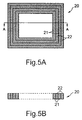
- Figs. 5A and 5B illustrate a complex adhesive sheet 20 made up from two electromagnetic shielding adhesive sheets 21 and two hermetically sealing adhesive sheets 22 that are alternately disposed. Such an alternate repetition of electromagnetic shielding and hermetic shielding according to this embodiment brings about an enhanced shielding effect.
- Fig. 6 is a flowchart for explaining a method of providing a complex adhesive paste to the MIC 10 as a shielding structure for a high frequency circuit according to the present invention.
- a conductive adhesive paste for electromagnetic shielding is printed on the joint surface of the metal stem 1 into a ring shape (step 1).
- an insulating adhesive paste is printed on the joint surface of the metal stem 1 into a ring shape outside the conductive adhesive (step 3).
- the metal stem 1 is heated to about 230 to 250°C (step 5).
- the metal cap 3 is put on the complex adhesive paste (step 6).
- weighting is performed from both the upper side of the metal cap 3 and the lower side of the metal stem 1 (step 7). Weighting in this case is desirably performed by about 20 to 30 kg.
- materials for combination of a conductive adhesive and an insulating adhesive having substantially the same glass transition temperature Tg are selected out of high polymer materials. Both are deformed at substantially the same temperature and joined by thermo-compression bonding.
- Each of the above-described shielding structures for a high frequency circuit according to the present invention does not have such a complicated shielding structure as includes application of a conductive adhesive to the joint between the metal stem and the metal cap, and welding of the whole periphery of the joint, which are performed conventionally. It affords the same electromagnetic shielding effect and hermetic seal effect as those of the conventional structure by only one joining operation with a complex adhesive. Therefore, the whole of the high frequency circuit can be easily manufactured.
- the sheet width or applied quantity of the hermetically sealing adhesive of the complex adhesive can be varied in accordance with hermetic seal condition. If the sheet width of the hermetically sealing adhesive is decreased for a high frequency circuit under an easy hermetic seal condition, a smaller size can be achieved.
Landscapes
- Engineering & Computer Science (AREA)
- Microelectronics & Electronic Packaging (AREA)
- Shielding Devices Or Components To Electric Or Magnetic Fields (AREA)
- Adhesives Or Adhesive Processes (AREA)
Applications Claiming Priority (2)
| Application Number | Priority Date | Filing Date | Title |
|---|---|---|---|
| JP11450099 | 1999-04-22 | ||
| JP11450099A JP3287330B2 (ja) | 1999-04-22 | 1999-04-22 | 高周波回路のシールド構造 |
Publications (2)
| Publication Number | Publication Date |
|---|---|
| EP1047295A2 true EP1047295A2 (fr) | 2000-10-25 |
| EP1047295A3 EP1047295A3 (fr) | 2002-01-02 |
Family
ID=14639317
Family Applications (1)
| Application Number | Title | Priority Date | Filing Date |
|---|---|---|---|
| EP00108005A Withdrawn EP1047295A3 (fr) | 1999-04-22 | 2000-04-19 | Structure de blindage haute fréquence et méthode |
Country Status (3)
| Country | Link |
|---|---|
| US (1) | US6462960B1 (fr) |
| EP (1) | EP1047295A3 (fr) |
| JP (1) | JP3287330B2 (fr) |
Cited By (2)
| Publication number | Priority date | Publication date | Assignee | Title |
|---|---|---|---|---|
| US7940944B2 (en) | 2006-05-09 | 2011-05-10 | Bse Co., Ltd. | Directional silicon condenser microphone having additional back chamber |
| US7949142B2 (en) | 2006-05-09 | 2011-05-24 | Bse Co., Ltd. | Silicon condenser microphone having additional back chamber and sound hole in PCB |
Families Citing this family (11)
| Publication number | Priority date | Publication date | Assignee | Title |
|---|---|---|---|---|
| AU3168601A (en) * | 2000-01-22 | 2001-07-31 | Helmut Kahl | Method for producing an electromagnetic shield |
| US6777613B2 (en) * | 2001-08-28 | 2004-08-17 | Nihon Dempa Kogyo Co., Ltd | Multifunctional crystal unit and method of manufacturing the same |
| US20040057198A1 (en) * | 2002-03-11 | 2004-03-25 | Helmut Kahl | Device housing comprising an electromagnetically shielded region |
| JP4024103B2 (ja) * | 2002-05-29 | 2007-12-19 | アルプス電気株式会社 | 高周波回路の接続構造 |
| US20040079549A1 (en) * | 2002-10-29 | 2004-04-29 | Yu Yuan Liang | Conductive substrate structure |
| WO2004044982A1 (fr) * | 2002-11-12 | 2004-05-27 | Fujitsu Limited | Structure d'emballage |
| US7070434B2 (en) * | 2004-07-27 | 2006-07-04 | Lockheed Martin Corporation | Rocket-launcher docking system |
| US7022911B1 (en) * | 2004-09-30 | 2006-04-04 | L3 Communications Corporation | Apparatus and method for providing electrostatic discharge protection |
| JP4555119B2 (ja) * | 2005-02-22 | 2010-09-29 | アルプス電気株式会社 | 面実装型電子回路ユニット |
| KR101664804B1 (ko) * | 2014-05-09 | 2016-10-11 | 이수호 | 방수용 기판스위치 및 방수용 기판스위치 제조방법 |
| US9900976B1 (en) * | 2016-12-12 | 2018-02-20 | Intel Corporation | Integrated circuit package including floating package stiffener |
Family Cites Families (14)
| Publication number | Priority date | Publication date | Assignee | Title |
|---|---|---|---|---|
| US3140342A (en) * | 1963-07-05 | 1964-07-07 | Chomerics Inc | Electrical shielding and sealing gasket |
| AT380410B (de) | 1984-10-15 | 1986-05-26 | Voest Alpine Ag | Kugelmuehle |
| JP2927010B2 (ja) * | 1991-03-01 | 1999-07-28 | 株式会社日立製作所 | 半導体パッケージ |
| CA2089435C (fr) * | 1992-02-14 | 1997-12-09 | Kenzi Kobayashi | Composant a semiconducteur |
| JP3362881B2 (ja) | 1992-11-17 | 2003-01-07 | 株式会社東芝 | 半導体パッケージ |
| JP2734424B2 (ja) | 1995-08-16 | 1998-03-30 | 日本電気株式会社 | 半導体装置 |
| US5761053A (en) * | 1996-05-08 | 1998-06-02 | W. L. Gore & Associates, Inc. | Faraday cage |
| TW486238U (en) * | 1996-08-18 | 2002-05-01 | Helmut Kahl | Shielding cap |
| EP0965255B2 (fr) * | 1997-03-05 | 2010-10-20 | Bernd Tiburtius | Procede pour fabriquer un boitier de blindage |
| US5982038A (en) * | 1997-05-01 | 1999-11-09 | International Business Machines Corporation | Cast metal seal for semiconductor substrates |
| US5821161A (en) * | 1997-05-01 | 1998-10-13 | International Business Machines Corporation | Cast metal seal for semiconductor substrates and process thereof |
| JP2845239B1 (ja) * | 1997-12-17 | 1999-01-13 | 日本電気株式会社 | 有機薄膜elデバイスおよびその製造方法 |
| JP3097644B2 (ja) * | 1998-01-06 | 2000-10-10 | 日本電気株式会社 | 半導体装置接続構造及び接続方法 |
| US6114761A (en) * | 1998-01-20 | 2000-09-05 | Lsi Logic Corporation | Thermally-enhanced flip chip IC package with extruded heatspreader |
-
1999
- 1999-04-22 JP JP11450099A patent/JP3287330B2/ja not_active Expired - Fee Related
-
2000
- 2000-04-19 EP EP00108005A patent/EP1047295A3/fr not_active Withdrawn
- 2000-04-20 US US09/552,883 patent/US6462960B1/en not_active Expired - Fee Related
Cited By (3)
| Publication number | Priority date | Publication date | Assignee | Title |
|---|---|---|---|---|
| US7940944B2 (en) | 2006-05-09 | 2011-05-10 | Bse Co., Ltd. | Directional silicon condenser microphone having additional back chamber |
| US7949142B2 (en) | 2006-05-09 | 2011-05-24 | Bse Co., Ltd. | Silicon condenser microphone having additional back chamber and sound hole in PCB |
| US7953235B2 (en) | 2006-05-09 | 2011-05-31 | Bse Co., Ltd. | Directional silicon condenser microphone having additional back chamber |
Also Published As
| Publication number | Publication date |
|---|---|
| JP3287330B2 (ja) | 2002-06-04 |
| US6462960B1 (en) | 2002-10-08 |
| EP1047295A3 (fr) | 2002-01-02 |
| JP2000307022A (ja) | 2000-11-02 |
Similar Documents
| Publication | Publication Date | Title |
|---|---|---|
| US5448106A (en) | Thin semiconductor integrated circuit device assembly | |
| US5252882A (en) | Surface acoustic wave device and its manufacturing method | |
| US6828663B2 (en) | Method of packaging a device with a lead frame, and an apparatus formed therefrom | |
| KR100256293B1 (ko) | 반도체장치 및 그 제조방법 | |
| US6462960B1 (en) | High frequency shielding structure and method | |
| US5619070A (en) | Semiconductor device which radiates heat and applies substrate potential from rear surface of semiconductor chip | |
| KR100397539B1 (ko) | 수지밀봉형 반도체 장치 및 그 제조방법 | |
| US7084723B2 (en) | Waveguide coupler | |
| KR970067892A (ko) | 고주파 집적회로장치 및 그 제조방법 | |
| US6770970B2 (en) | High-frequency module, method of manufacturing thereof and method of molding resin | |
| US5031022A (en) | Film carrier for mounting IC chips | |
| US7109583B2 (en) | Mounting with auxiliary bumps | |
| JP2970723B2 (ja) | 半導体パッケージおよびその製造方法 | |
| US6528347B2 (en) | Manufacturing method for making a microwave semiconductor device with improved heat discharge and electric properties | |
| KR100387451B1 (ko) | 반도체 장치 및 그 제조방법 | |
| US5767569A (en) | Tab tape and semiconductor chip mounted on tab tape | |
| US5541451A (en) | Packaged semiconductor device with external leads having anchor holes provided at polyamide/glass sealed regions | |
| USH1153H (en) | Non-metallized chip carrier | |
| KR100919985B1 (ko) | 반도체 팩키지용 필름 기판 및 이를 이용한 반도체 팩키지 | |
| KR950010733A (ko) | 멀티 칩 모듈 및 그 제조방법 | |
| JPS60200544A (ja) | 混成集積回路素子 | |
| JPH1174400A (ja) | Bga型半導体装置及びその製造方法 | |
| JPH04363901A (ja) | 高周波、マイクロ波用混成集積回路及びその製造方法 | |
| GB2300068A (en) | Semiconductor device | |
| JP2004319729A (ja) | 電子部品用パッケージ |
Legal Events
| Date | Code | Title | Description |
|---|---|---|---|
| PUAI | Public reference made under article 153(3) epc to a published international application that has entered the european phase |
Free format text: ORIGINAL CODE: 0009012 |
|
| AK | Designated contracting states |
Kind code of ref document: A2 Designated state(s): AT BE CH CY DE DK ES FI FR GB GR IE IT LI LU MC NL PT SE Kind code of ref document: A2 Designated state(s): DE FR GB |
|
| AX | Request for extension of the european patent |
Free format text: AL;LT;LV;MK;RO;SI |
|
| PUAL | Search report despatched |
Free format text: ORIGINAL CODE: 0009013 |
|
| AK | Designated contracting states |
Kind code of ref document: A3 Designated state(s): AT BE CH CY DE DK ES FI FR GB GR IE IT LI LU MC NL PT SE |
|
| AX | Request for extension of the european patent |
Free format text: AL;LT;LV;MK;RO;SI |
|
| 17P | Request for examination filed |
Effective date: 20011120 |
|
| AKX | Designation fees paid |
Free format text: DE FR GB |
|
| 17Q | First examination report despatched |
Effective date: 20021119 |
|
| STAA | Information on the status of an ep patent application or granted ep patent |
Free format text: STATUS: THE APPLICATION IS DEEMED TO BE WITHDRAWN |
|
| 18D | Application deemed to be withdrawn |
Effective date: 20030401 |