EP1049820B9 - Verfahren zur kristallzüchtung auf einem substrat - Google Patents
Verfahren zur kristallzüchtung auf einem substrat Download PDFInfo
- Publication number
- EP1049820B9 EP1049820B9 EP99956144A EP99956144A EP1049820B9 EP 1049820 B9 EP1049820 B9 EP 1049820B9 EP 99956144 A EP99956144 A EP 99956144A EP 99956144 A EP99956144 A EP 99956144A EP 1049820 B9 EP1049820 B9 EP 1049820B9
- Authority
- EP
- European Patent Office
- Prior art keywords
- conduit
- substrate
- process according
- growth
- reactor
- Prior art date
- Legal status (The legal status is an assumption and is not a legal conclusion. Google has not performed a legal analysis and makes no representation as to the accuracy of the status listed.)
- Expired - Lifetime
Links
- 239000000758 substrate Substances 0.000 title claims abstract description 65
- 238000000034 method Methods 0.000 title claims abstract description 39
- 230000012010 growth Effects 0.000 title claims abstract description 33
- 239000000463 material Substances 0.000 claims abstract description 95
- 239000013078 crystal Substances 0.000 claims abstract description 26
- 230000008018 melting Effects 0.000 claims abstract description 6
- 238000002844 melting Methods 0.000 claims abstract description 6
- 239000012768 molten material Substances 0.000 claims description 29
- 230000008569 process Effects 0.000 claims description 20
- HBMJWWWQQXIZIP-UHFFFAOYSA-N silicon carbide Chemical compound [Si+]#[C-] HBMJWWWQQXIZIP-UHFFFAOYSA-N 0.000 claims description 20
- 229910010271 silicon carbide Inorganic materials 0.000 claims description 19
- 239000002243 precursor Substances 0.000 claims description 9
- 150000001875 compounds Chemical class 0.000 claims description 8
- 239000007787 solid Substances 0.000 claims description 6
- 238000005229 chemical vapour deposition Methods 0.000 claims description 3
- 229910017083 AlN Inorganic materials 0.000 claims 1
- PIGFYZPCRLYGLF-UHFFFAOYSA-N Aluminum nitride Chemical compound [Al]#N PIGFYZPCRLYGLF-UHFFFAOYSA-N 0.000 claims 1
- 239000011343 solid material Substances 0.000 abstract 1
- 238000010438 heat treatment Methods 0.000 description 34
- 239000007789 gas Substances 0.000 description 32
- OKTJSMMVPCPJKN-UHFFFAOYSA-N Carbon Chemical compound [C] OKTJSMMVPCPJKN-UHFFFAOYSA-N 0.000 description 13
- 238000000151 deposition Methods 0.000 description 13
- 230000004927 fusion Effects 0.000 description 12
- 229910002804 graphite Inorganic materials 0.000 description 12
- 239000010439 graphite Substances 0.000 description 12
- 230000008021 deposition Effects 0.000 description 11
- PMHQVHHXPFUNSP-UHFFFAOYSA-M copper(1+);methylsulfanylmethane;bromide Chemical compound Br[Cu].CSC PMHQVHHXPFUNSP-UHFFFAOYSA-M 0.000 description 10
- 229910052582 BN Inorganic materials 0.000 description 9
- PZNSFCLAULLKQX-UHFFFAOYSA-N Boron nitride Chemical compound N#B PZNSFCLAULLKQX-UHFFFAOYSA-N 0.000 description 8
- XUIMIQQOPSSXEZ-UHFFFAOYSA-N Silicon Chemical compound [Si] XUIMIQQOPSSXEZ-UHFFFAOYSA-N 0.000 description 7
- 229910052710 silicon Inorganic materials 0.000 description 7
- 239000010703 silicon Substances 0.000 description 7
- IJGRMHOSHXDMSA-UHFFFAOYSA-N Atomic nitrogen Chemical compound N#N IJGRMHOSHXDMSA-UHFFFAOYSA-N 0.000 description 6
- 239000012159 carrier gas Substances 0.000 description 6
- 239000007788 liquid Substances 0.000 description 6
- 230000015572 biosynthetic process Effects 0.000 description 5
- 230000007935 neutral effect Effects 0.000 description 5
- 239000000470 constituent Substances 0.000 description 4
- 238000004519 manufacturing process Methods 0.000 description 4
- 241000894007 species Species 0.000 description 4
- 229910052782 aluminium Inorganic materials 0.000 description 3
- XAGFODPZIPBFFR-UHFFFAOYSA-N aluminium Chemical compound [Al] XAGFODPZIPBFFR-UHFFFAOYSA-N 0.000 description 3
- 229910052799 carbon Inorganic materials 0.000 description 3
- 239000000203 mixture Substances 0.000 description 3
- 229910052757 nitrogen Inorganic materials 0.000 description 3
- 229910052594 sapphire Inorganic materials 0.000 description 3
- 239000010980 sapphire Substances 0.000 description 3
- 238000010408 sweeping Methods 0.000 description 3
- 229910052715 tantalum Inorganic materials 0.000 description 3
- GUVRBAGPIYLISA-UHFFFAOYSA-N tantalum atom Chemical compound [Ta] GUVRBAGPIYLISA-UHFFFAOYSA-N 0.000 description 3
- QGZKDVFQNNGYKY-UHFFFAOYSA-N Ammonia Chemical compound N QGZKDVFQNNGYKY-UHFFFAOYSA-N 0.000 description 2
- XKRFYHLGVUSROY-UHFFFAOYSA-N Argon Chemical compound [Ar] XKRFYHLGVUSROY-UHFFFAOYSA-N 0.000 description 2
- ZOKXTWBITQBERF-UHFFFAOYSA-N Molybdenum Chemical compound [Mo] ZOKXTWBITQBERF-UHFFFAOYSA-N 0.000 description 2
- ATUOYWHBWRKTHZ-UHFFFAOYSA-N Propane Chemical compound CCC ATUOYWHBWRKTHZ-UHFFFAOYSA-N 0.000 description 2
- 239000004020 conductor Substances 0.000 description 2
- 238000001816 cooling Methods 0.000 description 2
- 238000007872 degassing Methods 0.000 description 2
- 230000004907 flux Effects 0.000 description 2
- 239000011810 insulating material Substances 0.000 description 2
- 239000007791 liquid phase Substances 0.000 description 2
- 229910052751 metal Inorganic materials 0.000 description 2
- 239000002184 metal Substances 0.000 description 2
- 229910052750 molybdenum Inorganic materials 0.000 description 2
- 239000011733 molybdenum Substances 0.000 description 2
- 230000003287 optical effect Effects 0.000 description 2
- 235000020004 porter Nutrition 0.000 description 2
- 239000011819 refractory material Substances 0.000 description 2
- 239000002470 thermal conductor Substances 0.000 description 2
- WFKWXMTUELFFGS-UHFFFAOYSA-N tungsten Chemical compound [W] WFKWXMTUELFFGS-UHFFFAOYSA-N 0.000 description 2
- 229910052721 tungsten Inorganic materials 0.000 description 2
- 239000010937 tungsten Substances 0.000 description 2
- ZOXJGFHDIHLPTG-UHFFFAOYSA-N Boron Chemical compound [B] ZOXJGFHDIHLPTG-UHFFFAOYSA-N 0.000 description 1
- UFHFLCQGNIYNRP-UHFFFAOYSA-N Hydrogen Chemical compound [H][H] UFHFLCQGNIYNRP-UHFFFAOYSA-N 0.000 description 1
- 238000004616 Pyrometry Methods 0.000 description 1
- 229910052581 Si3N4 Inorganic materials 0.000 description 1
- 229910000831 Steel Inorganic materials 0.000 description 1
- TZHYBRCGYCPGBQ-UHFFFAOYSA-N [B].[N] Chemical compound [B].[N] TZHYBRCGYCPGBQ-UHFFFAOYSA-N 0.000 description 1
- 229910021529 ammonia Inorganic materials 0.000 description 1
- 229910052786 argon Inorganic materials 0.000 description 1
- 244000052616 bacterial pathogen Species 0.000 description 1
- 238000009529 body temperature measurement Methods 0.000 description 1
- 229910052796 boron Inorganic materials 0.000 description 1
- 238000005234 chemical deposition Methods 0.000 description 1
- 239000003638 chemical reducing agent Substances 0.000 description 1
- 238000004581 coalescence Methods 0.000 description 1
- 230000008878 coupling Effects 0.000 description 1
- 238000010168 coupling process Methods 0.000 description 1
- 238000005859 coupling reaction Methods 0.000 description 1
- 238000000354 decomposition reaction Methods 0.000 description 1
- 238000009792 diffusion process Methods 0.000 description 1
- 238000009826 distribution Methods 0.000 description 1
- 230000000694 effects Effects 0.000 description 1
- 239000012777 electrically insulating material Substances 0.000 description 1
- 229940082150 encore Drugs 0.000 description 1
- 238000005265 energy consumption Methods 0.000 description 1
- 230000008020 evaporation Effects 0.000 description 1
- 238000001704 evaporation Methods 0.000 description 1
- 238000000605 extraction Methods 0.000 description 1
- 230000002349 favourable effect Effects 0.000 description 1
- 239000000835 fiber Substances 0.000 description 1
- 239000012530 fluid Substances 0.000 description 1
- 238000001657 homoepitaxy Methods 0.000 description 1
- 239000001257 hydrogen Substances 0.000 description 1
- 229910052739 hydrogen Inorganic materials 0.000 description 1
- 239000012535 impurity Substances 0.000 description 1
- 230000006698 induction Effects 0.000 description 1
- 238000012423 maintenance Methods 0.000 description 1
- 238000005259 measurement Methods 0.000 description 1
- 230000009347 mechanical transmission Effects 0.000 description 1
- 230000007246 mechanism Effects 0.000 description 1
- 239000013081 microcrystal Substances 0.000 description 1
- 229910021421 monocrystalline silicon Inorganic materials 0.000 description 1
- 150000004767 nitrides Chemical class 0.000 description 1
- 239000000615 nonconductor Substances 0.000 description 1
- 230000002093 peripheral effect Effects 0.000 description 1
- 239000001294 propane Substances 0.000 description 1
- 238000005086 pumping Methods 0.000 description 1
- 230000005855 radiation Effects 0.000 description 1
- 230000007420 reactivation Effects 0.000 description 1
- 229910000753 refractory alloy Inorganic materials 0.000 description 1
- 239000003870 refractory metal Substances 0.000 description 1
- 230000035040 seed growth Effects 0.000 description 1
- HQVNEWCFYHHQES-UHFFFAOYSA-N silicon nitride Chemical compound N12[Si]34N5[Si]62N3[Si]51N64 HQVNEWCFYHHQES-UHFFFAOYSA-N 0.000 description 1
- 239000010935 stainless steel Substances 0.000 description 1
- 229910001220 stainless steel Inorganic materials 0.000 description 1
- 239000010959 steel Substances 0.000 description 1
- 239000000126 substance Substances 0.000 description 1
- 230000008646 thermal stress Effects 0.000 description 1
- 239000012808 vapor phase Substances 0.000 description 1
Images



Classifications
-
- C—CHEMISTRY; METALLURGY
- C30—CRYSTAL GROWTH
- C30B—SINGLE-CRYSTAL GROWTH; UNIDIRECTIONAL SOLIDIFICATION OF EUTECTIC MATERIAL OR UNIDIRECTIONAL DEMIXING OF EUTECTOID MATERIAL; REFINING BY ZONE-MELTING OF MATERIAL; PRODUCTION OF A HOMOGENEOUS POLYCRYSTALLINE MATERIAL WITH DEFINED STRUCTURE; SINGLE CRYSTALS OR HOMOGENEOUS POLYCRYSTALLINE MATERIAL WITH DEFINED STRUCTURE; AFTER-TREATMENT OF SINGLE CRYSTALS OR A HOMOGENEOUS POLYCRYSTALLINE MATERIAL WITH DEFINED STRUCTURE; APPARATUS THEREFOR
- C30B25/00—Single-crystal growth by chemical reaction of reactive gases, e.g. chemical vapour-deposition growth
- C30B25/02—Epitaxial-layer growth
- C30B25/10—Heating of the reaction chamber or the substrate
- C30B25/105—Heating of the reaction chamber or the substrate by irradiation or electric discharge
-
- C—CHEMISTRY; METALLURGY
- C30—CRYSTAL GROWTH
- C30B—SINGLE-CRYSTAL GROWTH; UNIDIRECTIONAL SOLIDIFICATION OF EUTECTIC MATERIAL OR UNIDIRECTIONAL DEMIXING OF EUTECTOID MATERIAL; REFINING BY ZONE-MELTING OF MATERIAL; PRODUCTION OF A HOMOGENEOUS POLYCRYSTALLINE MATERIAL WITH DEFINED STRUCTURE; SINGLE CRYSTALS OR HOMOGENEOUS POLYCRYSTALLINE MATERIAL WITH DEFINED STRUCTURE; AFTER-TREATMENT OF SINGLE CRYSTALS OR A HOMOGENEOUS POLYCRYSTALLINE MATERIAL WITH DEFINED STRUCTURE; APPARATUS THEREFOR
- C30B11/00—Single-crystal growth by normal freezing or freezing under temperature gradient, e.g. Bridgman-Stockbarger method
-
- C—CHEMISTRY; METALLURGY
- C30—CRYSTAL GROWTH
- C30B—SINGLE-CRYSTAL GROWTH; UNIDIRECTIONAL SOLIDIFICATION OF EUTECTIC MATERIAL OR UNIDIRECTIONAL DEMIXING OF EUTECTOID MATERIAL; REFINING BY ZONE-MELTING OF MATERIAL; PRODUCTION OF A HOMOGENEOUS POLYCRYSTALLINE MATERIAL WITH DEFINED STRUCTURE; SINGLE CRYSTALS OR HOMOGENEOUS POLYCRYSTALLINE MATERIAL WITH DEFINED STRUCTURE; AFTER-TREATMENT OF SINGLE CRYSTALS OR A HOMOGENEOUS POLYCRYSTALLINE MATERIAL WITH DEFINED STRUCTURE; APPARATUS THEREFOR
- C30B11/00—Single-crystal growth by normal freezing or freezing under temperature gradient, e.g. Bridgman-Stockbarger method
- C30B11/002—Crucibles or containers for supporting the melt
-
- C—CHEMISTRY; METALLURGY
- C30—CRYSTAL GROWTH
- C30B—SINGLE-CRYSTAL GROWTH; UNIDIRECTIONAL SOLIDIFICATION OF EUTECTIC MATERIAL OR UNIDIRECTIONAL DEMIXING OF EUTECTOID MATERIAL; REFINING BY ZONE-MELTING OF MATERIAL; PRODUCTION OF A HOMOGENEOUS POLYCRYSTALLINE MATERIAL WITH DEFINED STRUCTURE; SINGLE CRYSTALS OR HOMOGENEOUS POLYCRYSTALLINE MATERIAL WITH DEFINED STRUCTURE; AFTER-TREATMENT OF SINGLE CRYSTALS OR A HOMOGENEOUS POLYCRYSTALLINE MATERIAL WITH DEFINED STRUCTURE; APPARATUS THEREFOR
- C30B11/00—Single-crystal growth by normal freezing or freezing under temperature gradient, e.g. Bridgman-Stockbarger method
- C30B11/003—Heating or cooling of the melt or the crystallised material
-
- C—CHEMISTRY; METALLURGY
- C30—CRYSTAL GROWTH
- C30B—SINGLE-CRYSTAL GROWTH; UNIDIRECTIONAL SOLIDIFICATION OF EUTECTIC MATERIAL OR UNIDIRECTIONAL DEMIXING OF EUTECTOID MATERIAL; REFINING BY ZONE-MELTING OF MATERIAL; PRODUCTION OF A HOMOGENEOUS POLYCRYSTALLINE MATERIAL WITH DEFINED STRUCTURE; SINGLE CRYSTALS OR HOMOGENEOUS POLYCRYSTALLINE MATERIAL WITH DEFINED STRUCTURE; AFTER-TREATMENT OF SINGLE CRYSTALS OR A HOMOGENEOUS POLYCRYSTALLINE MATERIAL WITH DEFINED STRUCTURE; APPARATUS THEREFOR
- C30B11/00—Single-crystal growth by normal freezing or freezing under temperature gradient, e.g. Bridgman-Stockbarger method
- C30B11/04—Single-crystal growth by normal freezing or freezing under temperature gradient, e.g. Bridgman-Stockbarger method adding crystallising materials or reactants forming it in situ to the melt
- C30B11/08—Single-crystal growth by normal freezing or freezing under temperature gradient, e.g. Bridgman-Stockbarger method adding crystallising materials or reactants forming it in situ to the melt every component of the crystal composition being added during the crystallisation
- C30B11/12—Vaporous components, e.g. vapour-liquid-solid-growth
-
- C—CHEMISTRY; METALLURGY
- C30—CRYSTAL GROWTH
- C30B—SINGLE-CRYSTAL GROWTH; UNIDIRECTIONAL SOLIDIFICATION OF EUTECTIC MATERIAL OR UNIDIRECTIONAL DEMIXING OF EUTECTOID MATERIAL; REFINING BY ZONE-MELTING OF MATERIAL; PRODUCTION OF A HOMOGENEOUS POLYCRYSTALLINE MATERIAL WITH DEFINED STRUCTURE; SINGLE CRYSTALS OR HOMOGENEOUS POLYCRYSTALLINE MATERIAL WITH DEFINED STRUCTURE; AFTER-TREATMENT OF SINGLE CRYSTALS OR A HOMOGENEOUS POLYCRYSTALLINE MATERIAL WITH DEFINED STRUCTURE; APPARATUS THEREFOR
- C30B19/00—Liquid-phase epitaxial-layer growth
-
- C—CHEMISTRY; METALLURGY
- C30—CRYSTAL GROWTH
- C30B—SINGLE-CRYSTAL GROWTH; UNIDIRECTIONAL SOLIDIFICATION OF EUTECTIC MATERIAL OR UNIDIRECTIONAL DEMIXING OF EUTECTOID MATERIAL; REFINING BY ZONE-MELTING OF MATERIAL; PRODUCTION OF A HOMOGENEOUS POLYCRYSTALLINE MATERIAL WITH DEFINED STRUCTURE; SINGLE CRYSTALS OR HOMOGENEOUS POLYCRYSTALLINE MATERIAL WITH DEFINED STRUCTURE; AFTER-TREATMENT OF SINGLE CRYSTALS OR A HOMOGENEOUS POLYCRYSTALLINE MATERIAL WITH DEFINED STRUCTURE; APPARATUS THEREFOR
- C30B29/00—Single crystals or homogeneous polycrystalline material with defined structure characterised by the material or by their shape
- C30B29/10—Inorganic compounds or compositions
- C30B29/36—Carbides
-
- C—CHEMISTRY; METALLURGY
- C30—CRYSTAL GROWTH
- C30B—SINGLE-CRYSTAL GROWTH; UNIDIRECTIONAL SOLIDIFICATION OF EUTECTIC MATERIAL OR UNIDIRECTIONAL DEMIXING OF EUTECTOID MATERIAL; REFINING BY ZONE-MELTING OF MATERIAL; PRODUCTION OF A HOMOGENEOUS POLYCRYSTALLINE MATERIAL WITH DEFINED STRUCTURE; SINGLE CRYSTALS OR HOMOGENEOUS POLYCRYSTALLINE MATERIAL WITH DEFINED STRUCTURE; AFTER-TREATMENT OF SINGLE CRYSTALS OR A HOMOGENEOUS POLYCRYSTALLINE MATERIAL WITH DEFINED STRUCTURE; APPARATUS THEREFOR
- C30B29/00—Single crystals or homogeneous polycrystalline material with defined structure characterised by the material or by their shape
- C30B29/10—Inorganic compounds or compositions
- C30B29/38—Nitrides
Definitions
- the invention relates to the field of layer deposition methods. thin and crystal growth of materials on a substrate.
- the invention also relates to a reactor for implementing this process.
- it may be a process for growing compounds binaries.
- Some binary compounds do not exist in a liquid state and also does not have large crystals of these compounds allowing a growth by homoepitaxy. This is particularly the case for silicon carbide (SiC) and aluminum nitride (AIN).
- crystals are obtained by the method Acheson, then they serve as germs to grow them by the method Lely.
- the crystals thus obtained are of very good crystalline quality but typically their dimensions are of the order of a centimeter. They are too much small for industrial exploitation, so a method of growth capable of growing them up to 5-10 cm.
- the so-called method modified Lely is currently the only industrial method of production of SiC under the 6H or 4H polytypes. It consists in sublimating a charge of granular SiC at 2300 ° C. and to condense it on a seed placed above at 2100 ° C. It is not without drawbacks especially because of the temperature at which growth should be done: 2300 ° C. The equipment to climb to these temperatures is very expensive and the difficulties encountered in increasing the size of the crystals are very large. Furthermore, the crystals obtained by this method have harmful microchannels for the production of large components of power.
- An object of the present invention is to provide a method and a reactor making it possible to improve the crystalline quality of crystals obtained by growth from a liquid phase on a substrate.
- the growth by points makes it possible to reduce the density of generally large dislocations, since the first material itself presents a lot of dislocations, for example because of a mesh mismatch between the first material and the substrate on which the first material is heteroepitaxied, while towards the ends of the tips, which is in the liquid, opposite the surface of the first material, it there is relaxation of constraints, which leads to a slight decrease in number of dislocations, but even at constant dislocation density, of made of the small surface of each point, this one presents only a few dislocations.
- the method according to the invention comprises a step consisting in reversing the direction of the temperature gradient.
- the invention also relates to a crystal growth reactor for the implementation of the method according to the invention, characterized in that it includes heating means making it possible to generate a gradient of temperature, perpendicular to the free surface of the molten material.
- the presence of a temperature gradient makes it possible to obtain spike growth extending in the direction of the gradient, rather that two-dimensional growth parallel to the plane of the first material.
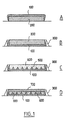
- a thin monocrystalline layer of the first material 100 is deposited on a substrate of a second material 200 by a conventional deposition method, known to those skilled in the art, by example a chemical vapor deposition.
- the substrate made of the second material 200 is monocrystalline silicon and the first material 100 is carbide of silicon.
- the monocrystalline layer of silicon carbide obtained has a high density of dislocations due to the disagreement of crystalline parameters between silicon and silicon carbide.
- step (b) the substrate and the layer deposited on it are placed, layer under substrate, horizontally in a special reactor at controlled vertical temperature gradient with no horizontal gradient.
- the height of crucible 300 is such that during the melting of the silicon substrate, the liquid does not exceed the edge of the crucible 300. This condition makes it possible to limit liquid leakage in the event of a break in the vertical edges of the layer of the first material 100 which is both a crucible and a seed growth.
- a neutral carrier gas for example argon
- argon is introduced into the reactor, preferably at a pressure equal to atmospheric pressure or more, to limit physical or reactive evaporation of the liquid consisting of second molten material 600, at a rate sufficient to ensure a almost uniform concentration of precursor gas over the entire substrate.
- step (c) the temperature is raised above the point of the second material 200, here silicon, ensuring a temperature on the free surface of the second molten material 600 lower than that of the interface between the first material 100 and the second 600 molten material.
- the thickness of the second molten material 600 above the first material 100 is advantageously of the order of a hundred or a few hundred micrometers, or even several millimeters.
- a precursor gas for example propane for SiC
- the precursor gas decomposes at the surface of the second molten material 600 and the first species atomic which it brings, here the carbon, diffuses towards the interface between the crystal tips and the second molten material 600 (Si) for participate in the growth of the fourth material 500, here the same as the first material 100, that is to say silicon carbide.
- Others components of the precursor gas are evacuated by the carrier gas to the exit from the reactor.
- stage (d) there is growth of the crystal points of the fourth material 500 on the layer of the first material 100, in the second molten material 600.
- the upper pressure limit partial of the precursor gas which must not be reached is that which would cause the formation of a continuous layer of the fourth material 500 on the surface of the second molten material 600, which would have the effect of instantly block any growth.
- This partial pressure limits depends on the temperature of the second molten material 600, it is typically 1000 Pascal.
- the crystal tips under the conditions defined above, are fairly evenly spaced and distributed.
- Step (e) is started when the crystal tips have reached a height of about 10 micrometers. It consists in reversing the sense of temperature gradient, i.e. the free surface of the second molten material 600 is brought to a temperature higher than that of the interface between the second molten material 600 and the first material 100, all the other parameters remaining identical. This causes a lateral growth of the fourth material 500, here SiC, from the top of the crystal points, which are continued during step (f).
- the fourth material 500 here SiC
- Step (f) is continued until the crystals coalesce into a thick monocrystalline layer.
- step (g) consisting in handing over a load of the second material 200 on the fourth material 500 to continue the growth in thickness.
- a charge of silicon is deposited on layer 700.
- the growth rate of the fourth material 500, typical as well obtained is several tens of micrometers per hour.
- the first 100 and fourth 500 materials are aluminum nitride
- the second material 200 is sapphire or silicon carbide
- the third material 400 is aluminum (Al).
- step (a ') aluminum nitride is deposited on sapphire, during step (a ').
- the sapphire substrate is placed in the crucible 300 with the aluminum nitride on top, during step (b ').
- Aluminum is brought to the liquid state on the aluminum nitride during step (c ').
- Ammonia or nitrogen are used as precursor gases in mixture with a carrier gas, to supply nitrogen, as the first species atomic, during step (d ').
- the rest of the process is equivalent to the one already described.
- the present invention makes it possible to produce SiC slices without microchannels, for example under polytypes 3C and 6H, large diameters (up to 200 mm and more), at a temperature of 1500 ° C instead of 2300 ° C, in a reactor inexpensive in investment and in cost of operation.
- SiC and AIN can be used for the growth of other binary compounds, as well as ternary compounds, etc.
- FIG. 3 A nonlimiting example of a reactor according to the invention is shown in FIG. 3.
- This reactor 1 comprises an enclosure 2 constituted by a tube 3, a first shutter 4 located at one end of this tube 3, and a outlet cross 5 located at the opposite end of the tube 3, with respect to the first shutter 4.
- the entire reactor 1 is sealed and can possibly withstand a pressure of a few MPa.
- the tightness of the reactor 1 is provided by seals 32, 33.
- the exit cross 5 can be replaced by an element in the form of "T".
- the axis of the tube 3 is horizontal. Inside the tube 3 is arranged a conduit 6 coaxial therewith Outside the tube 3 are arranged cooling means 11 able to cool the tube 3.
- the tube 3 is preferably a stainless steel cylinder.
- the cross 5 is preferably fixed because one of its outputs is connected to the pumping system.
- the outlet cross 5 has a lower hole and a hole upper, radially opposite in the vertical direction.
- the lower opening of this output cross 5 leads to a pump and a regulator of pressure for low pressures, either on a pressure reducer for a pressure higher than atmospheric pressure, in order to evacuate gas at constant pressure. These devices are not shown on the Figure 3 ..
- the upper opening of the outlet cross 5 is closed hermetically by a second shutter 26.
- the exit cross 5 furthermore has an orifice longitudinally opposite the tube 3. This orifice may optionally be fitted with a turning passage. In the mode of embodiment shown here, this orifice is closed by a third shutter 27 perpendicular to the axis of the tube 3.
- the third shutter 27 can possibly be fitted with a movable window or mirror for optical measurements inside the duct 6.
- This third shutter 27 has a hermetic door 28 for introducing or extracting substrates 10 of reactor 1.
- the third shutter 27 also includes guides 30, 31. These guides 30, 31 are perpendicular to the plane of the shutter 27 and are fixedly attached thereto. These guides 30, 31 are used to guide horizontally a manipulator not shown on the FIGS.
- the third shutter 27 also includes passages for first current leads 22, 23. The parts of the first leads current 22, 23, located towards the inside of enclosure 2, are provided with connectors 24, 25.
- a conduit 6 is positioned and maintained in the tube 3 by means of fixing means 35 of the duct 6 on the first shutter 4. Thus, the conduit 6 is held so as to be free from contact with the tube 3. Which limits heat conduction losses and avoids thermal stresses.
- the conduit 6 has the form of a tube to rectangular cross section, having a narrowing 36 to a end of it.
- This conduit 6 has two plates to form the bottom 37 and top 38 walls.
- Bottom 37 and top walls 38 of the conduit 6 are horizontal and parallel to the plane of the substrate 10 in the position he occupies during the deposit.
- Side walls 39, 40 join the longitudinal edges of the lower 37 and upper 38 walls to close the conduit 6 longitudinally.
- the end of the conduit 6 located on the side of the constriction 36 has a square cross section.
- She is provided with a support plate 41 perpendicular to the longitudinal axis of the conduit 6. This support plate 41 has an opening facing the mouth of the conduit 6 located on the side of the narrowing 36.
- the plate support 41 also has holes for fixing the duct 6 on the first shutter 4, thanks to the fixing means 35.
- the mouth of conduit 6 located on the side of the narrowing 36 and the opening in the support plate 41 are located opposite a gas inlet 7.
- the duct 6 is connected tightly sealed to the first shutter 4, at the gas inlet 7.
- the sealed connection of the conduit 6 on the first shutter 4 is provided by tightening of a graphite joint for example, by means of fixing 35.
- the gas inlet 7 is used to supply the reactor 1 with carrier gases and precursors.
- the first shutter 4 is also provided with a gas passage 44, offset from the axis of symmetry perpendicular to the plane of the disc which constitutes the first obturator 4, and emerging between the duct 6 and the wall of the tube 3.
- the gas passage 44 also allows the introduction of gas in reactor 1.
- the gas passage 44 makes it possible to circulate a neutral gas vis-à-vis all of the materials included in reactor 1 and vis-à-vis the material to be deposited and the gases flowing in the conduit 6, this neutral gas preventing the possible return of gases from the process to the heating parts outside the duct 6.
- the conduit 6 is made of a material which is both good thermal conductor, good electrical insulator, very refractory, very chemically stable and has a low vapor pressure at temperatures of use, although possibly, prior deposition of the material intended to be deposited on a substrate 10 in this reactor 1, is produced on the face internal walls 37, 38, 39, 40 of conduit 6, in order to minimize diffusion any degassing products during normal operation of the reactor 1.
- this material has good resistance mechanical to tolerate a small thickness of the walls 37, 38, 39, 40 of the conduit 6.
- the small thickness of these walls 37, 38, 39, 40 makes it possible to minimize losses by thermal conduction and thermal inertia.
- the mechanical strength of the material of the conduit 6 is also important. to be able to support this conduit 6 only by its end located on the side of the constriction 36 and the support plate 41.
- the material constituting the conduit 6 is advantageously nitride boron for use at temperatures below 1200 ° C or below higher temperatures, if the presence of a high concentration of nitrogen does not harm the expected quality of the material produced.
- the conduit 6 can be made in graphite.
- the conduit 6 can be doubled internally in the hottest parts by a secondary duct of a refractory material, for example of refractory metal, inert with respect to gases circulating in the conduit 6 and non-polluting vis-à-vis the material deposit.
- Line 6, whether it is made of graphite or boron nitride, can be produced either by pyrolytic deposition or by assembling and / or bonding different constituent plates of the walls 37, 38, 39, 40 and of the plate support 41.
- the secondary duct when it exists, doubles advantageously internally the conduit 6 continuously, it is to say that if it consists of plates, these are contiguous and that there is no holes in these plates.
- the secondary duct is, for example, in tungsten, tantalum, molybdenum, graphite or boron nitride.
- the thickness of the walls of the conduit 6 is less or equal to about 1 mm; the internal height of duct 6 is preferably less than 30 mm; the width of the duct 6 is equal to the width of a substrate 10 or the sum of the widths of the substrates 10 treated during the same deposit, plus approximately 1 cm between the substrate (s) 10 and walls 39 and 40.
- the part of the conduit 6 corresponding to the narrowing 36 corresponds to approximately 1/5 of the total length of conduit 6.
- the length of the constant section of the duct 6 is approximately five times the diameter or length of the largest substrate 10 to be used, or five times the sum of the diameters or lengths of the substrates 10 over which can be deposited during the same transaction.
- This part of the conduit 6 extending over a length corresponding to the diameter or the length of a substrate or the sum of the lengths or substrate diameters, is called the deposition zone below.
- the reactor 1 is provided with first 8 and second 9 heating means, arranged at the deposition zone and located on either side of the plane of the substrate 10.
- these first 8 and second 9 means of heating consist of bare resistive elements, that is to say that the constituent material of the first 8 and second 9 heating means is in direct contact with the gas circulating between the conduit 6 and the tube 3.
- Each resistive element corresponding respectively to the first 8 or the second 9 heating means consists of a strip, that is to say a rigid plate element, or a ribbon arranged flat, parallel to the lower 37 and upper 38 walls of the conduit 6 (fig. 4).
- This ribbon or this strip has a geometry adapted so that, in the area deposit, deviations from average temperature, on the surface of the substrate 10 intended for deposit, are minimized. Preferably still, these deviations are less than 3 ° C.
- each resistive element has a dimension in the direction parallel to the width of the conduit 6 which is approximately equal to the latter. The dimension of each element resistive in the direction parallel to the length of the conduit 6 is approximately equal to twice the length of the drop zone. This to optimize uniformity of the temperature field in the deposition area.
- each strip or ribbon of a resistive element is made up of strips parallel to each other, in the direction longitudinal of the tube 3, joined two by two alternately to one or the other of their ends, so as to form a zigzag geometry.
- Other geometries are possible, such as spiral geometries.
- Each resistive element can have a longitudinal profile of resistance for example obtained by playing on its thickness, suitable for favor the formation of a controlled temperature profile in the deposit.
- Each resistive element has a large filling coefficient in the deposit area so that their temperature remains as low as possible higher than the desired local temperature.
- the space between the strips of the resistive elements is sufficient to avoid an arc or short circuit, but is weak enough also to maintain an acceptable temperature field homogeneity and for that it doesn't have to be much higher than that of the conduit which is itself the one to which the deposit is made.
- the first 8 and second 9 heating means are supplied at a voltage less than or equal to 240 volts and more preferably still less, or equal to 100, 110 or 120 volts.
- the first 8 and second 9 means of heaters each consist of several resistive elements of the type of those described above.
- the resistive elements are produced in a conductive and refractory material with very low vapor pressure at operating temperatures.
- This material can for example be graphite. a metal such as tantalum or tungsten, or a refractory alloy, etc.
- it is this high purity graphite.
- the first 8 and second 9 heating means are supplied by running independently of each other, so that it can be brought to different temperatures. We can also generate a gradient of temperature perpendicular to the plane of the substrate 10. This gradient can be of positive, negative or zero value by independent control of the electrical power applied to one of the first 8 or second 9 heating means.
- the first 8 or second 9 heating means can be applied in contact with the lower 37 and upper 38 walls, outside the conduit 6, at the deposition zone. But according to a preferred variant these are each positioned respectively at a distance of 1 to 3 mm from one of the lower 37 or upper 38 walls, outside the duct 6.
- the first 8 and the second 9 means of heating are kept pressed against the lower walls 37 and upper 38 by the electrically insulating retaining plates 12, 13 and thermally conductive.
- the conduit 6 is not a electrically insulating material, it is necessary to put between the conduit 6 and the first 8 and second 9 heating means, a material intermediate, electrically insulating, to avoid electrical contact, especially in the hot zone, if very high temperatures are to be reached.
- thermocouples 51 can be glued to the retaining plates 12, 13, but they can also be free above the first 8 and second 9 heating means.
- thermocouples (not shown in Figures 3 to 5) are used to measure the temperature of line 6, to regulate it and to control its homogeneity in the drop zone.
- thermocouples 51 can be used for temperatures below 1700 ° C (for temperatures above 1700 ° C, the temperature should be measured by optical pyrometry or by thermocouples without contacts).
- the hot weld of these thermocouples 51 is located at the outside of conduit 6 as close as possible to the first 8 and second 9 means of heating.
- the first 8 and second 9 heating means can be made of rigid graphite. They are then electrically isolated from conduit 6 by wedges, for example made of boron nitride, which separate them from line 6 of a few millimeters. These shims can be attached to the ends of the first 8 and second 9 heating means and therefore not to be too heated.
- One or more graphite or boron nitride sheaths can be fixed on the faces of the conduit 6 to receive thermocouples themselves insulated in refractory and insulating sheaths electrically.
- each cradle 16, 17 consists of two parallel half-discs, one to each other and connected together by rods which are perpendicular to them.
- the diameter of the discs, consisting of two half-discs, corresponds approximately the internal diameter of the tube 3.
- the straight edge of the two half discs is in a horizontal plane.
- Each straight edge of each half-disc includes notches capable of accommodating a plate 12 or 13, the first 8 or the second 9 means of heating, as well as half the height of duct 6.
- the elements resistives of the first 8 and second 9 heating means are required isolated from the conduit 6 by the cradles 16, 17.
- the half discs of the cradles 16, 17 are at contact of the conduit 6 in the cold parts thereof.
- Heat shields 14, 15 are placed on either side of the first 8 and second 9 heating means, outside of these last. More specifically, heat shields 15 are located between the inner wall of tube 3 and the curvilinear part of the constituent half-discs cages 16, 17. They extend under the internal face of the tube 3, but without contact with it, concentrically, around the area of heater. Other heat shields 14 are placed between the plates of maintenance 12, 13 and the preceding 15. These heat shields 14, 15 are composed of two or three thin sheets of reflective polished metal and refractory such as tantalum, molybdenum, etc. The heat shield 14 or 15 the outermost is as close as possible to a few millimeters from the inner wall of the tube 3. This longitudinal configuration, with the first 8 and second 19 heating means inside the tube 3, in contact with the conduit 6, and two or three heat shields 14, 15 greatly limit losses by radiation which would otherwise be very important at high temperatures, such as those required for deposition of silicon carbide.
- the half-discs of the cradles 16, 17 are formed in a electrically and thermally insulating material. So the screens 14, 15 are electrically and thermally insulated from each other and heating means 8, 9.
- This assembly limits the gas circulation outside the hot part of the duct and participates thus limiting thermal losses.
- two discs 18, 19 are placed between the cradles 16, 17 and the outlet cross 5, perpendicular to the axis of the tube 3.
- these discs 18, 19 are provided with a rectangular central opening with corresponding surface approximately at the cross section of the duct 6, so that being able to thread these discs 18, 19 onto this conduit 6. These discs 18, 19 also have peripheral holes in the central opening, intended for passage of second current leads 20, 21, and wires of thermocouples 51.
- One 19 of these discs 18, 19 is placed in the cross of output 5. The other 18 of these discs 18, 19 is placed between the disc 19 and the cradles 16, 17.
- These discs 18, 19 both have the role of maintaining the conduit 6, second current leads 20, 21 and the wires of thermocouples 51, as well as that of limiting gas exchanges between inside the duct 6 and the space between the duct 6 and the tube 3.
- the discs 18, 19 must allow passage of the gases, in coming from the outlet of conduit 6, between the interior space of conduit 6 and the space between the conduit 6 and the tube 3, so that the pressure is balanced on both sides of the walls 37, 38, 39, 40. In thus balancing the pressure on either side of the walls 37, 38, 39, 40, it is allowed to realize these with a small thickness.
- the pairs of the second current leads 20, 21 are connected to the first current leads 22, 23 thanks to the connectors 24, 25.
- the thermocouples 51 are also connected to outside of enclosure 2 via connectors located in enclosure 2.
- the discs 18, 19 can be made of an insulating material electrically and thermally but not necessarily very refractory.
- the hermetic door 28 covers an opening whose width is approximately equal to that of the duct. This opening is located in the axis of the conduit 6. It allows the introduction and the extraction of the substrates 10.
- An entry airlock is possibly connected to the third shutter 27 to avoid the reactivation of reactor 1 during operations for introducing and extracting the substrates 10,
- the substrates 10 are advantageously introduced into the reactor 1 thanks to a substrate holder 29.
- the substrate holder 29 is advantageously made of a good thermal conductor material so that it has little thermal inertia.
- this substrate holder 29 is produced boron nitride but it can also be graphite for example.
- the substrate holder 29 is introduced into reactor 1 by a gripper manipulator which slides on the guides 30, 31.
- This manipulator consists of a thin tube and rigid coaxial with the axis of conduit 6, a long threaded rod inside this tube, integral with the side of reactor 1, of two clamp elements symmetrical and articulated around a vertical hinge, the end outside of the threaded rod being screwed into a rotating captive nut freely.
- the threaded rod moves back and the clamp tightens firmly on a vertical part of the substrate holder 29.
- the manipulator can then be moved along the guides 30, 31 to introduce or extract the substrate holder 29.
- a cam on the manipulator can be provided to allow the clamp to be raised, when the clamp has just gripped the substrate holder 29, in its position inside the duct 6, so that the latter does not rub the internal face of the wall 37.
- a deposit of the product majority to which the reactor 1 is dedicated is deposited in line 6 without substrate 10, or substrate holder 29, after extensive degassing, at a temperature higher than usual deposition temperature and sweeping by the carrier gas. This step can be followed by a similar deposit on the substrate holder 29 without substrate 10. The reactor is then ready for use.
- the process and the reactor according to the invention can be the subject of variants.
- the current leads 22, 23 and thermocouple outputs can advantageously be located on the same side as the gas inlet 7.
- the loading and unloading of substrates 10 can then be done by separating the body of reactor 3 from the cross 5. It is then interesting to put a rotating substrate holder 29 actuated by a rotating passage watertight and motorized axially passing through the shutter 27. This arrangement is particularly useful in steps (a) and (a ') of the methods described above.
- first 8 and second 9 means of resistive heating.
- This type of heating means allows to rise to temperatures above 1750 ° C, with low investment in materials and lower energy consumption than with processes and prior art reactors
- a power of 3 kW is sufficient.
- a power line of 7 kW is also sufficient.
- heating 8, 9 even if these appear less advantageous, such as induction heating means, heating means in which the first 8 and second 9 heating means 9 do not form that a single device arranged all around the duct 6, etc.
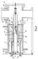
- FIG. 6 shows another embodiment of the reactor 1 according to the invention.
- the reactor 1 includes an enclosure 2 consisting of two steel tubes 3, 103 stainless, concentric, whose common axis of revolution is horizontal. In the space between the two walls of these tubes 3, 103 circulates a cooling.
- a jet breaker 50 is mounted in the axis of the gas inlet 7 so to promote the obtaining of a good uniformity of the speed of the gases.
- the gas passage 44 can also optionally be provided with a jet breaker.
- All electrical and fluid connections on the third shutter 27 and the first shutter 4 are sufficiently long and flexible to be able to move them about twice the length of the conduit 6.
- connections can also be made only on the first shutter 4.
- the first shutter 4 is integral with a carriage comprising a vertical support 64 and horizontal support 65.
- the horizontal support 65 can be moved parallel to the axis of the tube 3, on a raceway not shown. In order to climb the entire duct 6 and its equipment, the first shutter 4 is open, the tube 3 remaining integral with the cross 5.
- the substrates 10 are introduced and maintained in the deposition zone by a graphite substrate holder 29 which can be lifted by a few degrees, on the downstream side with respect to the gas flow, so as to offer a larger projection surface on a vertical plane, in the duct 6.
- the substrate holder is for example made up of a disc with a rim.
- the rim is advantageously of a height greater than the height of the substrate 10.
- the substrate holder 29 can rotate the substrate 10 that it supports, so as to ensure better uniformity of the deposit. This is advantageously done, thanks to a mechanical transmission, consisting of a bevel gear of horizontal axis and integral with the shaft 61, it even in rotation thanks to a motor external to reactor 1, at speed variable ensuring a substrate rotation speed of up to 10 turns per second.
- the reactor in accordance with the present invention comprises first 8 and second heating means, offset from each other in the longitudinal direction of the conduit 6. This also makes it possible to homogenize the distribution of the temperature over the entire surface of the substrate, favoring the formation of a plateau in the longitudinal temperature profile.
- the center of the substrate 10 on the substrate holder 29 is offset downstream of the gas flow, in the area of first 8 and second 9 heating means, without however that the substrate 10 does not leave this zone.
- the conduit secondary consists of removable 70 plates, which can be inserted and easily removed by sliding in grooves not shown in the conduit 6.
- These plates 70 are useful for protecting conduit 6 from deposits out of the substrate (s) 10. They are easy to maintain and are advantageously made of graphite, boron nitride or another material refractory compatible with the process temperature and the ambient environment.
- the temperature can be measured by fibers 71 of pyrometers optics located in sheaths integral with the conduit 6 and between the conduit 6 and the first 8 and second 9 heating means, rather than by thermocouples 51, this in order to increase the lifetime of the means of temperature measurement.
- the method according to the invention makes it possible to obtain the abovementioned advantages while retaining a level of impurities in the layers obtained equivalent to those of the layers obtained by the processes and prior art reactors.
- a process and a reactor according to the invention are particularly well suitable for growing layers of silicon carbide or nitride aluminum on substrates 10.
Landscapes
- Chemical & Material Sciences (AREA)
- Engineering & Computer Science (AREA)
- Crystallography & Structural Chemistry (AREA)
- Materials Engineering (AREA)
- Metallurgy (AREA)
- Organic Chemistry (AREA)
- Inorganic Chemistry (AREA)
- Chemical Kinetics & Catalysis (AREA)
- General Chemical & Material Sciences (AREA)
- Crystals, And After-Treatments Of Crystals (AREA)
- Chemical Vapour Deposition (AREA)
- Liquid Deposition Of Substances Of Which Semiconductor Devices Are Composed (AREA)
Claims (11)
- Kristallwachstumsverfahren um ein Material auf einem ersten festen Material (100) anwachsen zu lassen, ausgehend von einem geschmolzenen Material auf dem ersten festen Material (100), gekennzeichnet durch:einen Schritt (a), um das erste Materials (100) auf einem Substrat (10) anwachsen zu lassen, das aus einem zweiten Material (200) besteht,ein Schritt (d, d'), bei welchem man, ausgehend von der Schnittfläche zwischen dem ersten Matrial (100) und dem geschmolzenen Material, Kristallnadeln bestehend aus dem ersten Material (100) anwachsen läßt, wobei ein Temperaturgradient in senkrechter Richtung zur freien Oberfläche des geschmolzenen Materials auferlegt wird, derart daß die Schnittstelle zwischen dem ersten Material und dem geschmolzenen Material eine Temperatur aufweist, die größer ist als die Temperatur an der freien Oberfläche des geschmolzenen Materials,einen Schritt (f,f'), der darin besteht, ausgehend von den Kristallnadeln Kristalle in einer zur freien Ebene des geschmolzenen Materials weitgehend parallelen Ebene lateral anwachsen zu lassen, indem das Vorzeichen des Temperaturgradienten umgekehrt wird.
- Verfahren nach dem vorangehenden Anspruch, dadurch gekennzeichnet, daß es einen Schritt (b) umfaßt, der darin besteht, das Substrat horizontal in einen Schmelztiegel (300) zu plazieren derart, daß das erste Material (100) unter dem zweiten Material (200) liegt.
- Verfahren nach einem der Ansprüche 1 oder 2, dadurch gekennzeichnet, daß es einen Schritt (b') umfaßt, der darin besteht, das Substrat horizontal in einen Schmelztiegel (300) zu plazieren derart, daß das erste Material (100) unter dem zweiten Material (200) liegt und auf dem ersten ein drittes Material (400) liegt.
- Verfahren nach Anspruch 2, dadurch gekennzeichnet, daß es einen Schritt (c) umfaßt, der darin besteht, daß das zweite Material (200) zum Schmelzen gebracht wird, wobei das erste Matrial (100) im festen Zustand gehalten wird.
- Verfahren nach Anspruch 3, dadurch gekennzeichnet, daß es einen Schritt (c') umfaßt, der darin besteht, daß das dritte Material (400) zum Schmelzen gebracht wird, wobei das erste Matrial (100) und das zweite Material (200) in festem Zustand gehalten werden.
- Verfahren nach einem der vorangehenden Anspüchen, dadurch gekennzeichnet, daß es einen Schritt (d, d') umfaßt, bei welchem das geschmolzene Material mit einem Vorstufengas beströmt wird, dessen mindestens eine erste Atomsorte mit mindestens einer zweiten, aus dem geschmolzenen Material stammenden Atomsorte, am Wachstum eines vierten Materials (500) teilhaben.
- Verfahren nach Anspruch 6, dadurch gekennzeichnet, daß das vierte Material (500) eine Binärverbindung ist.
- Verfahren nach Anspruch 7, dadurch gekennzeichnet, daß die Binärverbindung aus Siliziumkarbid besteht.
- Verfahren nach Anspruch 7, dadurch gekennzeichnet, daß die Binärverbindung aus Aluminiumnitrid besteht.
- Verfahren nach einem der Ansprüche 6 bis 9, dadurch gekennzeichnet, daß es einen Schritt (g, g') umfaßt, der darin besteht, nocheinmal eine Menge eines zweiten (200) oder des dritten Materials (400) auf das vierte Material (500) aufzutragen, um das Dickenwachstum fortzusetzen.
- Verfahren nach einem der Ansprüche 1 bis 10, dadurch gekennzeichnet, daß der Schritt (a, a') durch chemische Dampfabscheidung realisiert wird.
Applications Claiming Priority (5)
| Application Number | Priority Date | Filing Date | Title |
|---|---|---|---|
| FR9814831 | 1998-11-25 | ||
| FR9814831A FR2786203B1 (fr) | 1998-11-25 | 1998-11-25 | Reacteur pour depot chimique en phase vapeur et procede pour sa mise en oeuvre |
| FR9905840A FR2786208B1 (fr) | 1998-11-25 | 1999-05-07 | Procede de croissance cristalline sur substrat et reacteur pour sa mise en oeuvre |
| FR9905840 | 1999-05-07 | ||
| PCT/FR1999/002910 WO2000031322A1 (fr) | 1998-11-25 | 1999-11-25 | Procede de croissance cristalline sur substrat |
Publications (3)
| Publication Number | Publication Date |
|---|---|
| EP1049820A1 EP1049820A1 (de) | 2000-11-08 |
| EP1049820B1 EP1049820B1 (de) | 2003-08-20 |
| EP1049820B9 true EP1049820B9 (de) | 2004-07-14 |
Family
ID=26234675
Family Applications (2)
| Application Number | Title | Priority Date | Filing Date |
|---|---|---|---|
| EP99956143A Expired - Lifetime EP1049813B1 (de) | 1998-11-25 | 1999-11-25 | Cvd-reaktor und verfahren zum betrieb desselben |
| EP99956144A Expired - Lifetime EP1049820B9 (de) | 1998-11-25 | 1999-11-25 | Verfahren zur kristallzüchtung auf einem substrat |
Family Applications Before (1)
| Application Number | Title | Priority Date | Filing Date |
|---|---|---|---|
| EP99956143A Expired - Lifetime EP1049813B1 (de) | 1998-11-25 | 1999-11-25 | Cvd-reaktor und verfahren zum betrieb desselben |
Country Status (9)
| Country | Link |
|---|---|
| US (2) | US6402836B1 (de) |
| EP (2) | EP1049813B1 (de) |
| JP (2) | JP2002530266A (de) |
| KR (2) | KR100643062B1 (de) |
| AU (2) | AU1280500A (de) |
| DE (2) | DE69910540T2 (de) |
| ES (1) | ES2205903T3 (de) |
| FR (1) | FR2786208B1 (de) |
| WO (2) | WO2000031317A1 (de) |
Families Citing this family (15)
| Publication number | Priority date | Publication date | Assignee | Title |
|---|---|---|---|---|
| AU2001245270A1 (en) * | 2000-02-15 | 2001-09-03 | The Fox Group, Inc. | Method and apparatus for growing low defect density silicon carbide and resulting material |
| US6896738B2 (en) * | 2001-10-30 | 2005-05-24 | Cree, Inc. | Induction heating devices and methods for controllably heating an article |
| FR2833619A1 (fr) * | 2001-12-17 | 2003-06-20 | Commissariat Energie Atomique | Procede de fabrication de substrats semi-conducteurs cristallins |
| FR2836159B1 (fr) * | 2002-02-15 | 2004-05-07 | Centre Nat Rech Scient | Procede de formation de couche de carbure de silicium ou de nitrure d'element iii sur un substrat adapte |
| US7473873B2 (en) * | 2004-05-18 | 2009-01-06 | The Board Of Trustees Of The University Of Arkansas | Apparatus and methods for synthesis of large size batches of carbon nanostructures |
| TW200609371A (en) * | 2004-05-18 | 2006-03-16 | Univ Arkansas | Apparatus and methods of making nanostructures by inductive heating |
| US7365289B2 (en) * | 2004-05-18 | 2008-04-29 | The United States Of America As Represented By The Department Of Health And Human Services | Production of nanostructures by curie point induction heating |
| US7404858B2 (en) * | 2005-09-16 | 2008-07-29 | Mississippi State University | Method for epitaxial growth of silicon carbide |
| KR100893408B1 (ko) * | 2007-08-22 | 2009-04-17 | 주식회사 테라세미콘 | 기판 홀더 |
| US10407769B2 (en) | 2016-03-18 | 2019-09-10 | Goodrich Corporation | Method and apparatus for decreasing the radial temperature gradient in CVI/CVD furnaces |
| CN105749832A (zh) * | 2016-04-21 | 2016-07-13 | 常州大学 | 一种具有脉冲变径微结构的微反应器系统 |
| DK4273296T3 (da) | 2016-07-15 | 2025-06-10 | Oned Mat Inc | Fremstillingsanordning og fremgangsmåde til fremstilling af siliciumnanowirer på carbonbaserede pulvere til anvendelse i batterier |
| US10632447B2 (en) * | 2018-08-28 | 2020-04-28 | Molecule Works Inc. | Reactor for hydrothermal growth of structured materials |
| TWI860350B (zh) * | 2019-04-26 | 2024-11-01 | 學校法人關西學院 | 碳化矽半導體基板、碳化矽半導體基板的製造方法、碳化矽半導體基板的製造裝置以及磊晶成長方法 |
| KR102500070B1 (ko) * | 2021-03-30 | 2023-02-15 | 주식회사 테스 | 유기금속화학기상증착장치 |
Family Cites Families (37)
| Publication number | Priority date | Publication date | Assignee | Title |
|---|---|---|---|---|
| GB1139802A (en) * | 1964-10-30 | 1969-01-15 | Mini Of Technology | Growth of crystalline layers |
| GB1332348A (en) * | 1970-11-19 | 1973-10-03 | Nat Res Corp | Silicon carbide junction diode |
| JPS5583226A (en) | 1978-12-19 | 1980-06-23 | Fujitsu Ltd | Gas phase growing device |
| US4582561A (en) * | 1979-01-25 | 1986-04-15 | Sharp Kabushiki Kaisha | Method for making a silicon carbide substrate |
| JPS5645897A (en) * | 1979-09-19 | 1981-04-25 | Sharp Corp | Manufacture of silicon carbide crystal |
| US4315479A (en) * | 1980-06-27 | 1982-02-16 | Atomel Corporation | Silicon wafer steam oxidizing apparatus |
| JPS58139424A (ja) | 1982-02-15 | 1983-08-18 | Hitachi Ltd | 気相成長装置 |
| JPS58158914A (ja) * | 1982-03-16 | 1983-09-21 | Semiconductor Res Found | 半導体製造装置 |
| US4423701A (en) * | 1982-03-29 | 1984-01-03 | Energy Conversion Devices, Inc. | Glow discharge deposition apparatus including a non-horizontally disposed cathode |
| JPS59928A (ja) * | 1982-06-25 | 1984-01-06 | Ushio Inc | 光加熱装置 |
| US4601260A (en) * | 1985-04-01 | 1986-07-22 | Sovonics Solar Systems | Vertical semiconductor processor |
| US4614672A (en) * | 1985-06-06 | 1986-09-30 | The United States Of America As Represented By The Secretary Of The Navy | Liquid phase epitaxy (LPE) of silicon carbide |
| FR2591616A1 (fr) * | 1985-12-17 | 1987-06-19 | Labo Electronique Physique | Chambre de reacteur pour croissance epitaxiale en phase vapeur des materiaux semiconducteurs. |
| US4747367A (en) * | 1986-06-12 | 1988-05-31 | Crystal Specialties, Inc. | Method and apparatus for producing a constant flow, constant pressure chemical vapor deposition |
| US5221556A (en) * | 1987-06-24 | 1993-06-22 | Epsilon Technology, Inc. | Gas injectors for reaction chambers in CVD systems |
| DE3721636A1 (de) | 1987-06-30 | 1989-01-12 | Aixtron Gmbh | Quarzglasreaktor fuer mocvd-anlagen |
| JPH0676275B2 (ja) * | 1988-07-21 | 1994-09-28 | 三菱電機株式会社 | 気相エピタキシャル成長装置および基板の加熱方法 |
| US5194401A (en) * | 1989-04-18 | 1993-03-16 | Applied Materials, Inc. | Thermally processing semiconductor wafers at non-ambient pressures |
| US5108792A (en) * | 1990-03-09 | 1992-04-28 | Applied Materials, Inc. | Double-dome reactor for semiconductor processing |
| JPH0547674A (ja) | 1991-08-13 | 1993-02-26 | Fujitsu Ltd | 気相成長装置および気相成長方法 |
| US5336324A (en) * | 1991-12-04 | 1994-08-09 | Emcore Corporation | Apparatus for depositing a coating on a substrate |
| US5253324A (en) * | 1992-09-29 | 1993-10-12 | North Carolina State University | Conical rapid thermal processing apparatus |
| TW337513B (en) | 1992-11-23 | 1998-08-01 | Cvd Inc | Chemical vapor deposition-produced silicon carbide having improved properties and preparation process thereof |
| US5298287A (en) | 1993-02-05 | 1994-03-29 | United Technologies Corporation | Method of making CVD Si3 N4 |
| JP3190165B2 (ja) * | 1993-04-13 | 2001-07-23 | 東京エレクトロン株式会社 | 縦型熱処理装置及び熱処理方法 |
| JP3008782B2 (ja) * | 1994-07-15 | 2000-02-14 | 信越半導体株式会社 | 気相成長方法およびその装置 |
| JPH0897159A (ja) * | 1994-09-29 | 1996-04-12 | Handotai Process Kenkyusho:Kk | エピタキシャル成長方法および成長装置 |
| JP3444991B2 (ja) | 1994-10-14 | 2003-09-08 | 東海カーボン株式会社 | セラミックス被膜の形成方法 |
| SE9500327D0 (sv) | 1995-01-31 | 1995-01-31 | Abb Research Ltd | Device for epitaxially growing SiC by CVD |
| US6002109A (en) * | 1995-07-10 | 1999-12-14 | Mattson Technology, Inc. | System and method for thermal processing of a semiconductor substrate |
| SE9600705D0 (sv) * | 1996-02-26 | 1996-02-26 | Abb Research Ltd | A susceptor for a device for epitaxially growing objects and such a device |
| JP3493880B2 (ja) | 1996-02-28 | 2004-02-03 | 信越半導体株式会社 | 輻射加熱装置および加熱方法 |
| US6133550A (en) * | 1996-03-22 | 2000-10-17 | Sandia Corporation | Method and apparatus for thermal processing of semiconductor substrates |
| US5759263A (en) * | 1996-12-05 | 1998-06-02 | Abb Research Ltd. | Device and a method for epitaxially growing objects by cvd |
| US5879459A (en) * | 1997-08-29 | 1999-03-09 | Genus, Inc. | Vertically-stacked process reactor and cluster tool system for atomic layer deposition |
| US6121061A (en) * | 1997-11-03 | 2000-09-19 | Asm America, Inc. | Method of processing wafers with low mass support |
| US6303906B1 (en) * | 1999-11-30 | 2001-10-16 | Wafermasters, Inc. | Resistively heated single wafer furnace |
-
1999
- 1999-05-07 FR FR9905840A patent/FR2786208B1/fr not_active Expired - Fee Related
- 1999-11-25 WO PCT/FR1999/002909 patent/WO2000031317A1/fr not_active Ceased
- 1999-11-25 AU AU12805/00A patent/AU1280500A/en not_active Abandoned
- 1999-11-25 JP JP2000584126A patent/JP2002530266A/ja active Pending
- 1999-11-25 DE DE69910540T patent/DE69910540T2/de not_active Expired - Lifetime
- 1999-11-25 US US09/600,904 patent/US6402836B1/en not_active Expired - Fee Related
- 1999-11-25 US US09/601,109 patent/US6709520B1/en not_active Expired - Lifetime
- 1999-11-25 KR KR1020007008111A patent/KR100643062B1/ko not_active Expired - Fee Related
- 1999-11-25 JP JP2000584124A patent/JP4693993B2/ja not_active Expired - Lifetime
- 1999-11-25 EP EP99956143A patent/EP1049813B1/de not_active Expired - Lifetime
- 1999-11-25 DE DE69932919T patent/DE69932919T2/de not_active Expired - Lifetime
- 1999-11-25 EP EP99956144A patent/EP1049820B9/de not_active Expired - Lifetime
- 1999-11-25 KR KR1020007008116A patent/KR100747940B1/ko not_active Expired - Lifetime
- 1999-11-25 WO PCT/FR1999/002910 patent/WO2000031322A1/fr not_active Ceased
- 1999-11-25 AU AU12806/00A patent/AU1280600A/en not_active Abandoned
- 1999-11-25 ES ES99956144T patent/ES2205903T3/es not_active Expired - Lifetime
Also Published As
| Publication number | Publication date |
|---|---|
| KR20010040406A (ko) | 2001-05-15 |
| AU1280600A (en) | 2000-06-13 |
| FR2786208B1 (fr) | 2001-02-09 |
| JP2002530266A (ja) | 2002-09-17 |
| WO2000031317A1 (fr) | 2000-06-02 |
| JP4693993B2 (ja) | 2011-06-01 |
| KR20010040405A (ko) | 2001-05-15 |
| EP1049813A1 (de) | 2000-11-08 |
| KR100643062B1 (ko) | 2006-11-10 |
| EP1049820A1 (de) | 2000-11-08 |
| US6402836B1 (en) | 2002-06-11 |
| DE69910540D1 (de) | 2003-09-25 |
| JP2002530265A (ja) | 2002-09-17 |
| ES2205903T3 (es) | 2004-05-01 |
| EP1049820B1 (de) | 2003-08-20 |
| WO2000031322A1 (fr) | 2000-06-02 |
| KR100747940B1 (ko) | 2007-08-08 |
| EP1049813B1 (de) | 2006-08-23 |
| AU1280500A (en) | 2000-06-13 |
| DE69910540T2 (de) | 2004-06-24 |
| FR2786208A1 (fr) | 2000-05-26 |
| DE69932919D1 (de) | 2006-10-05 |
| DE69932919T2 (de) | 2007-08-30 |
| US6709520B1 (en) | 2004-03-23 |
Similar Documents
| Publication | Publication Date | Title |
|---|---|---|
| EP1049820B9 (de) | Verfahren zur kristallzüchtung auf einem substrat | |
| EP0312447B1 (de) | Verfahren und Anlage zur Herstellung dünner Schichten mittels eines Plasmas für elektronische bzw. opto-elektronische Anwendungen | |
| FR2628985A1 (fr) | Reacteur d'epitaxie a paroi protegee contre les depots | |
| FR2543980A1 (fr) | Procede de fabrication de materiaux semiconducteurs et four de traitement pour la mise en oeuvre de ce procede | |
| CN112466929B (zh) | 碳化硅衬底、晶锭及其制备方法 | |
| FR2929959A1 (fr) | Procede de preparation de polycristaux et de monocristaux d'oxyde de zinc (zno) sur un germe par sublimation activee chimiquement a haute temperature | |
| EP0005442B1 (de) | Verfahren und Vorrichtung zur Herstellung von Aluminiumnitrid, das für elektronische Anwendungen geeignet ist | |
| EP0801155A1 (de) | Verfahren und Vorrichtung zur Herstellung einkristallines Siliziumkarbids (SiC) auf einem Keimkristall | |
| FR2484469A1 (fr) | Procede de preparation de couches homogenes de hg1-xcdxte | |
| EP1415023B1 (de) | Verfahren zur herstellung eines einkristalles aus cdte oder cdznte | |
| FR2540892A1 (fr) | Procede et dispositif de chauffage de substrat pour l'epitaxie par jet moleculaire | |
| EP0743377A1 (de) | Vorrichtung zur chemischen Oberflächenbehandlung eines flachen Substrates mittels aktiver Gase | |
| FR2530267A1 (fr) | Procede et appareil pour effectuer la croissance epitaxiale d'un cristal de znse a partir de znse fondu | |
| CA2486662C (en) | Vapor-phase growth apparatus | |
| FR2786203A1 (fr) | Reacteur pour depot chimique en phase vapeur et procede pour sa mise en oeuvre | |
| EP0223629B1 (de) | Verfahren und Vorrichtung zur Bildung eines dünnen Films durch Abscheidung aus der Gasphase auf mehreren Substratflächen | |
| von Münch et al. | New susceptor arrangement for the epitaxial growth of β-SiC on silicon | |
| FR2620135A1 (fr) | Procede de croissance d'un cristal de silicium en forme de ruban de structure dendritique | |
| CN113417006B (zh) | 一种提高籽晶质量的制备装置及方法 | |
| FR2655772A1 (fr) | Dispositif antipollution pour bati vertical de depot en phase gazeuse. | |
| EP4634969A1 (de) | Verfahren zur stabilisierung einer oberfläche eines halbleitermaterials | |
| FR2610450A1 (fr) | Dispositif de traitement thermique de plaquettes semi-conductrices | |
| WO2025196157A1 (fr) | Procede de traitement d'un substrat presentant une surface en un materiau semiconducteur | |
| EP0119130B1 (de) | Transparente Heizvorrichtung mit wenigstens zwei Zonen mit verschiedenen Temperaturen | |
| WO2025068410A1 (fr) | Procede de traitement d'un substrat de carbure de silicium |
Legal Events
| Date | Code | Title | Description |
|---|---|---|---|
| PUAI | Public reference made under article 153(3) epc to a published international application that has entered the european phase |
Free format text: ORIGINAL CODE: 0009012 |
|
| AK | Designated contracting states |
Kind code of ref document: A1 Designated state(s): AT BE CH CY DE DK ES FI FR GB GR IE IT LI LU MC NL PT SE |
|
| 17P | Request for examination filed |
Effective date: 20001129 |
|
| 17Q | First examination report despatched |
Effective date: 20020528 |
|
| GRAH | Despatch of communication of intention to grant a patent |
Free format text: ORIGINAL CODE: EPIDOS IGRA |
|
| GRAH | Despatch of communication of intention to grant a patent |
Free format text: ORIGINAL CODE: EPIDOS IGRA |
|
| RAP1 | Party data changed (applicant data changed or rights of an application transferred) |
Owner name: CENTRE NATIONAL DE LA RECHERCHE SCIENTIFIQUE (CNRS |
|
| GRAA | (expected) grant |
Free format text: ORIGINAL CODE: 0009210 |
|
| AK | Designated contracting states |
Designated state(s): DE ES FR GB IT NL |
|
| REG | Reference to a national code |
Ref country code: GB Ref legal event code: FG4D Free format text: NOT ENGLISH |
|
| REF | Corresponds to: |
Ref document number: 69910540 Country of ref document: DE Date of ref document: 20030925 Kind code of ref document: P |
|
| GBT | Gb: translation of ep patent filed (gb section 77(6)(a)/1977) |
Effective date: 20031204 |
|
| REG | Reference to a national code |
Ref country code: ES Ref legal event code: FG2A Ref document number: 2205903 Country of ref document: ES Kind code of ref document: T3 |
|
| PLBE | No opposition filed within time limit |
Free format text: ORIGINAL CODE: 0009261 |
|
| STAA | Information on the status of an ep patent application or granted ep patent |
Free format text: STATUS: NO OPPOSITION FILED WITHIN TIME LIMIT |
|
| 26N | No opposition filed |
Effective date: 20040524 |
|
| NLR4 | Nl: receipt of corrected translation in the netherlands language at the initiative of the proprietor of the patent | ||
| PGFP | Annual fee paid to national office [announced via postgrant information from national office to epo] |
Ref country code: ES Payment date: 20091106 Year of fee payment: 11 Ref country code: DE Payment date: 20091126 Year of fee payment: 11 |
|
| PGFP | Annual fee paid to national office [announced via postgrant information from national office to epo] |
Ref country code: NL Payment date: 20091103 Year of fee payment: 11 |
|
| PGFP | Annual fee paid to national office [announced via postgrant information from national office to epo] |
Ref country code: IT Payment date: 20091031 Year of fee payment: 11 Ref country code: GB Payment date: 20091102 Year of fee payment: 11 Ref country code: FR Payment date: 20091214 Year of fee payment: 11 |
|
| REG | Reference to a national code |
Ref country code: NL Ref legal event code: V1 Effective date: 20110601 |
|
| GBPC | Gb: european patent ceased through non-payment of renewal fee |
Effective date: 20101125 |
|
| REG | Reference to a national code |
Ref country code: DE Ref legal event code: R119 Ref document number: 69910540 Country of ref document: DE Effective date: 20110601 Ref country code: DE Ref legal event code: R119 Ref document number: 69910540 Country of ref document: DE Effective date: 20110531 |
|
| REG | Reference to a national code |
Ref country code: FR Ref legal event code: ST Effective date: 20110801 |
|
| PG25 | Lapsed in a contracting state [announced via postgrant information from national office to epo] |
Ref country code: NL Free format text: LAPSE BECAUSE OF NON-PAYMENT OF DUE FEES Effective date: 20110601 |
|
| PG25 | Lapsed in a contracting state [announced via postgrant information from national office to epo] |
Ref country code: DE Free format text: LAPSE BECAUSE OF NON-PAYMENT OF DUE FEES Effective date: 20110531 |
|
| PG25 | Lapsed in a contracting state [announced via postgrant information from national office to epo] |
Ref country code: FR Free format text: LAPSE BECAUSE OF NON-PAYMENT OF DUE FEES Effective date: 20101130 |
|
| PG25 | Lapsed in a contracting state [announced via postgrant information from national office to epo] |
Ref country code: GB Free format text: LAPSE BECAUSE OF NON-PAYMENT OF DUE FEES Effective date: 20101125 |
|
| PG25 | Lapsed in a contracting state [announced via postgrant information from national office to epo] |
Ref country code: IT Free format text: LAPSE BECAUSE OF NON-PAYMENT OF DUE FEES Effective date: 20101125 |
|
| REG | Reference to a national code |
Ref country code: ES Ref legal event code: FD2A Effective date: 20120110 |
|
| PG25 | Lapsed in a contracting state [announced via postgrant information from national office to epo] |
Ref country code: ES Free format text: LAPSE BECAUSE OF NON-PAYMENT OF DUE FEES Effective date: 20101126 |