EP1052575A1 - Système de transmission, récepteur et réseau d'interconnexion - Google Patents
Système de transmission, récepteur et réseau d'interconnexion Download PDFInfo
- Publication number
- EP1052575A1 EP1052575A1 EP00201579A EP00201579A EP1052575A1 EP 1052575 A1 EP1052575 A1 EP 1052575A1 EP 00201579 A EP00201579 A EP 00201579A EP 00201579 A EP00201579 A EP 00201579A EP 1052575 A1 EP1052575 A1 EP 1052575A1
- Authority
- EP
- European Patent Office
- Prior art keywords
- modules
- neighboring
- data
- calculation
- direct chain
- Prior art date
- Legal status (The legal status is an assumption and is not a legal conclusion. Google has not performed a legal analysis and makes no representation as to the accuracy of the status listed.)
- Withdrawn
Links
Images
Classifications
-
- G—PHYSICS
- G06—COMPUTING OR CALCULATING; COUNTING
- G06F—ELECTRIC DIGITAL DATA PROCESSING
- G06F12/00—Accessing, addressing or allocating within memory systems or architectures
-
- G—PHYSICS
- G06—COMPUTING OR CALCULATING; COUNTING
- G06F—ELECTRIC DIGITAL DATA PROCESSING
- G06F15/00—Digital computers in general; Data processing equipment in general
- G06F15/16—Combinations of two or more digital computers each having at least an arithmetic unit, a program unit and a register, e.g. for a simultaneous processing of several programs
- G06F15/163—Interprocessor communication
- G06F15/173—Interprocessor communication using an interconnection network, e.g. matrix, shuffle, pyramid, star, snowflake
- G06F15/17337—Direct connection machines, e.g. completely connected computers, point to point communication networks
Definitions
- the present invention describes a transmission system, a receiver and a programmable network architecture to interconnect different receiver components located on a direct chain and a return path, so as to make communications to very high speed which may include feedback loops.
- a system, a receiver and a network are provided such as mentioned in the preamble, remarkable in that said local communications and are carried out by a series of programmable interconnection cells comprising storage means for storing the data passing between two non-neighboring modules located on at least the direct chain or the return path.
- each cell interconnection is connected to at least one calculation module, called the current module, and comprises multiplexing means connected to neighboring cells for multiplexing data from different modules on the direct chain and the return channel, said storage means being connected to the multiplexing means respectively upstream and downstream of said module current for said data to pass through two neighboring cells at the more, in one calculation cycle.
- the calculation modules can be different filtering units set up cascade, to achieve for example: an anti-aliasing filter, a Nyquist filter and an Equalizer.
- an anti-aliasing filter Several successive digital filterings are indeed necessary, in particular in digital television to provide the demodulation function.
- these demodulations require feedback loops to synchronize the receiver with the transmitter.
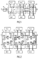
- the invention proposes a particularly well suited architecture for an interconnection network modular with programmable interconnection cells C1, C2 and C3 provided storage means 11, 12 and 13 respectively for storing the transmitted data between two non-neighboring calculation modules so that they pass through two at most neighboring cells in one calculation cycle.
- FIG 2 shows in more detail an embodiment for the receiver of Figure 1 and the interconnection network 11 according to the invention.
- An object of the invention is to define an interconnection network having a simple topology capable of operating at high frequency.
- the connections use in general multiplexers or data buses to multiplex data from different calculation modules on the different communication chains.
- a bus does not allows to communicate only one data in a clock cycle.
- Network topology interconnection according to the invention is defined so that all the calculation blocks can provide and receive data at each cycle.
- the communication time between two neighboring modules being one clock cycle, the data transfer time depends on the distance traveled by this data and therefore the number of multiplexers crossed in a clock cycle.
- the invention provides means to guarantee that the data does not pass through more than two multiplexers in a clock cycle.
- the return path being capable of being used in counter flanges reaction, local communications can therefore be carried out between two neighboring modules on the feedback loop, i.e. between two modules facing each other, one located on the direct chain and the other on the way back.
- FIG. 2 illustrates an example of application which implements data communications, shown in thick hatched lines, between the FU2 modules and FU3 in the forward direction and which carries out a feedback loop involving the BU2 modules and BU3 on the return chain.
- This may for example be data communications between different elements of a digital television receiver to perform channel decoding.
- the cell comprises a total of four MUX multiplexers controlled by a control member, not shown, provided with a clock for multiplexing the data coming from the different modules FU i and BU i from the different communication chains.
- a first memory MD is connected to the two multiplexers MUX 1 and MUX 2 which are located on the direct chain, respectively upstream and downstream of the direct current module FU i and a second memory MR, called return memory, is connected to the two multiplexers MUX 3 and MUX 4 on the return channel, located respectively upstream and downstream of the current return module BU i .
- the first multiplexer MUX 1 has a first input to receive data from the direct chain, a second input to receive data from the feedback loop and an output connected to the direct memory MD and the current module FU i of the direct chain.
- the second multiplexer MUX 2 has a first input to receive the data stored in the direct memory MD, a second input to receive the data provided by the current module of the direct chain FU i and an output to transmit the input data multiplexed on the direct chain and on the return chain via the feedback loop.
- the third MUX multiplexer 3 has a first input for receiving data from the output of the second MUX multiplexer 2 , a second input for receiving data from the return chain of the neighboring cell and an output connected to the return memory MR and to the current calculation module on the return chain BU i .
- the fourth multiplexer MUX 4 has a first input for receiving the data stored in the return memory MR, a second input for receiving the data provided by the current module of the return chain BU i and an output for transmitting the input data multiplexed on the return chain and on the direct chain via the feedback loop.
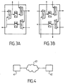
- FIG. 3 represents two alternative embodiments of the interconnection cells according to the invention comprising three programmable multiplexers MUX 1 , MUX 2 and MUX 3 .
- Figure 3A illustrates an example of degraded cell usable for applications where it lacks a calculation module on the return chain. The degraded cell is directly connected to only one module on the direct chain. The output of the third multiplexer MUX 3 is connected only to the register MR. The output of the register MR is connected to an input of the first multiplexer MUX 1 and to the return channel of the next cell.
- FIG. 3B illustrates an example of degraded cell usable for applications comprising a direct reaction between two modules FU and BU vis-à-vis on the direct chain and on the return chain.
- the input of the first multiplexer MUX 1 is directly connected to an output of a module for calculating the return chain BU and the output of the register MR is only connected to the next cell on the return channel.
- Figure 4 is a general diagram of a transmission system according to invention comprising a transmitter 41, a receiver 42 of the type shown in the figure 1 and a transmission channel 43 to support for example satellite transmissions, by cable or over the air, etc.
Landscapes
- Engineering & Computer Science (AREA)
- Computer Hardware Design (AREA)
- Theoretical Computer Science (AREA)
- Physics & Mathematics (AREA)
- General Engineering & Computer Science (AREA)
- General Physics & Mathematics (AREA)
- Mathematical Physics (AREA)
- Software Systems (AREA)
- Data Exchanges In Wide-Area Networks (AREA)
- Small-Scale Networks (AREA)
- Mobile Radio Communication Systems (AREA)
- Cable Transmission Systems, Equalization Of Radio And Reduction Of Echo (AREA)
Applications Claiming Priority (2)
| Application Number | Priority Date | Filing Date | Title |
|---|---|---|---|
| FR9906020A FR2793628A1 (fr) | 1999-05-11 | 1999-05-11 | Systeme de transmission, recepteur et reseau d'interconnexion |
| FR9906020 | 1999-05-11 |
Publications (1)
| Publication Number | Publication Date |
|---|---|
| EP1052575A1 true EP1052575A1 (fr) | 2000-11-15 |
Family
ID=9545487
Family Applications (1)
| Application Number | Title | Priority Date | Filing Date |
|---|---|---|---|
| EP00201579A Withdrawn EP1052575A1 (fr) | 1999-05-11 | 2000-05-02 | Système de transmission, récepteur et réseau d'interconnexion |
Country Status (6)
| Country | Link |
|---|---|
| US (1) | US6839357B1 (ja) |
| EP (1) | EP1052575A1 (ja) |
| JP (1) | JP2000358046A (ja) |
| KR (1) | KR100653111B1 (ja) |
| CN (1) | CN1147101C (ja) |
| FR (1) | FR2793628A1 (ja) |
Families Citing this family (5)
| Publication number | Priority date | Publication date | Assignee | Title |
|---|---|---|---|---|
| JP3801559B2 (ja) * | 2002-12-26 | 2006-07-26 | ソニー株式会社 | 通信装置および方法、記録媒体、並びにプログラム |
| TWI269992B (en) | 2004-03-22 | 2007-01-01 | Aten Int Co Ltd | The keyboard video mouse switch for multiply chaining and the switching method of signals thereof |
| US7415595B2 (en) * | 2005-05-24 | 2008-08-19 | Coresonic Ab | Data processing without processor core intervention by chain of accelerators selectively coupled by programmable interconnect network and to memory |
| US7725792B2 (en) * | 2006-03-01 | 2010-05-25 | Qualcomm Incorporated | Dual-path, multimode sequential storage element |
| US11144497B2 (en) | 2018-08-16 | 2021-10-12 | Tachyum Ltd. | System and method of populating an instruction word |
Citations (4)
| Publication number | Priority date | Publication date | Assignee | Title |
|---|---|---|---|---|
| US4334305A (en) * | 1979-02-15 | 1982-06-08 | Cselt - Centro Studi E Laboratori Telecomunicazioni S.P.A. | Data-handling system with operatively interconnected processors |
| US4663706A (en) * | 1982-10-28 | 1987-05-05 | Tandem Computers Incorporated | Multiprocessor multisystem communications network |
| US5050065A (en) * | 1987-11-06 | 1991-09-17 | Thomson-Csf | Reconfigurable multiprocessor machine for signal processing |
| US5689661A (en) * | 1993-03-31 | 1997-11-18 | Fujitsu Limited | Reconfigurable torus network having switches between all adjacent processor elements for statically or dynamically splitting the network into a plurality of subsystems |
Family Cites Families (2)
| Publication number | Priority date | Publication date | Assignee | Title |
|---|---|---|---|---|
| US5937202A (en) * | 1993-02-11 | 1999-08-10 | 3-D Computing, Inc. | High-speed, parallel, processor architecture for front-end electronics, based on a single type of ASIC, and method use thereof |
| US6456628B1 (en) * | 1998-04-17 | 2002-09-24 | Intelect Communications, Inc. | DSP intercommunication network |
-
1999
- 1999-05-11 FR FR9906020A patent/FR2793628A1/fr not_active Withdrawn
-
2000
- 2000-05-02 EP EP00201579A patent/EP1052575A1/fr not_active Withdrawn
- 2000-05-08 JP JP2000134366A patent/JP2000358046A/ja not_active Abandoned
- 2000-05-08 CN CNB001181661A patent/CN1147101C/zh not_active Expired - Fee Related
- 2000-05-10 US US09/568,285 patent/US6839357B1/en not_active Expired - Fee Related
- 2000-05-10 KR KR1020000024879A patent/KR100653111B1/ko not_active Expired - Fee Related
Patent Citations (4)
| Publication number | Priority date | Publication date | Assignee | Title |
|---|---|---|---|---|
| US4334305A (en) * | 1979-02-15 | 1982-06-08 | Cselt - Centro Studi E Laboratori Telecomunicazioni S.P.A. | Data-handling system with operatively interconnected processors |
| US4663706A (en) * | 1982-10-28 | 1987-05-05 | Tandem Computers Incorporated | Multiprocessor multisystem communications network |
| US5050065A (en) * | 1987-11-06 | 1991-09-17 | Thomson-Csf | Reconfigurable multiprocessor machine for signal processing |
| US5689661A (en) * | 1993-03-31 | 1997-11-18 | Fujitsu Limited | Reconfigurable torus network having switches between all adjacent processor elements for statically or dynamically splitting the network into a plurality of subsystems |
Also Published As
| Publication number | Publication date |
|---|---|
| CN1147101C (zh) | 2004-04-21 |
| KR100653111B1 (ko) | 2006-12-04 |
| US6839357B1 (en) | 2005-01-04 |
| FR2793628A1 (fr) | 2000-11-17 |
| CN1273476A (zh) | 2000-11-15 |
| JP2000358046A (ja) | 2000-12-26 |
| KR20010014890A (ko) | 2001-02-26 |
Similar Documents
| Publication | Publication Date | Title |
|---|---|---|
| FR2979444A1 (fr) | Reseau sur puce extensible | |
| FR2860313A1 (fr) | Composant a architecture reconfigurable dynamiquement | |
| FR3032078A1 (fr) | Architecture hybride de transmission d'informations avioniques et systeme correspondant | |
| FR2687814A1 (fr) | Processeur neuronal a cellules synaptiques reparties. | |
| EP3084588A1 (fr) | Module de traitement du signal, notamment pour reseau de neurones et circuit neuronal. | |
| FR2510763A1 (fr) | Dispositif d'interconnexion d'une serie d'appareils d'acquisition de donnees a un systeme de reception et d'enregistrement eloigne | |
| EP1052575A1 (fr) | Système de transmission, récepteur et réseau d'interconnexion | |
| EP0715437A1 (fr) | Procédé d'acheminement de cellules dans un réseau ATM | |
| FR2494868A1 (fr) | Circuit logique permettant une operation d'essai | |
| FR2865290A1 (fr) | Procede de gestion de donnees dans un processeur matriciel et processeur matriciel mettant en oeuvre ce procede | |
| FR3045893A1 (fr) | Circuit electronique, notamment apte a l'implementation de reseaux de neurones a plusieurs niveaux de precision. | |
| FR2890766A1 (fr) | Systeme et procede de communication asynchrone sur circuit, entre des sous-circuits synchrones | |
| CA2619301A1 (fr) | Passerelle de communication entre deux entites | |
| FR2981477A1 (fr) | Systeme d'au moins un ensemble comprenant au moins un circuit integre, lesdits circuits integres etant interconnectes selon une architecture matricielle, muni d'au moins une interconnexion optique | |
| EP1175121A1 (fr) | Dispositif de commutation permettant une diffusion | |
| FR2527882A1 (fr) | Concentrateur numerique | |
| EP4002801B1 (fr) | Procédé de communication de l'état d'un réseau de calculateur(s), programme d'ordinateur, noeud de calcul et réseau associés | |
| EP2989721A1 (fr) | Dispositif cascadable de reception numerique multi voies | |
| FR2596606A1 (fr) | Commutateur a architecture modulaire | |
| FR2525781A1 (fr) | Dispositif de sondage ultrasonore a balayage electronique | |
| FR2470495A1 (fr) | Systeme de commutation numerique de telecommunications capable d'etablir des connexions multilaterales de teleconference et de diffusion selective d'informations ou de signaux | |
| FR2475328A1 (fr) | Systeme de commutation numerique de telecommunications, equipe de moyens de connexion en conference d'un ou plusieurs groupes de terminaux | |
| WO1993025976A1 (fr) | Processeur parallele pour traitement de multiples donnees par une serie d'instructions repetitives | |
| FR3009466A1 (fr) | Reseau sur puce multiprocesseur | |
| FR2528646A1 (fr) | Dispositif de transmission entre les terminaisons d'un systeme de communication temporel |
Legal Events
| Date | Code | Title | Description |
|---|---|---|---|
| PUAI | Public reference made under article 153(3) epc to a published international application that has entered the european phase |
Free format text: ORIGINAL CODE: 0009012 |
|
| AK | Designated contracting states |
Kind code of ref document: A1 Designated state(s): DE ES FR GB IT |
|
| AX | Request for extension of the european patent |
Free format text: AL;LT;LV;MK;RO;SI |
|
| 17P | Request for examination filed |
Effective date: 20010515 |
|
| AKX | Designation fees paid |
Free format text: DE ES FR GB IT |
|
| 17Q | First examination report despatched |
Effective date: 20060920 |
|
| GRAP | Despatch of communication of intention to grant a patent |
Free format text: ORIGINAL CODE: EPIDOSNIGR1 |
|
| STAA | Information on the status of an ep patent application or granted ep patent |
Free format text: STATUS: THE APPLICATION IS DEEMED TO BE WITHDRAWN |
|
| 18D | Application deemed to be withdrawn |
Effective date: 20080828 |