EP1052697B1 - Photodiodenanordnung - Google Patents
Photodiodenanordnung Download PDFInfo
- Publication number
- EP1052697B1 EP1052697B1 EP00109551A EP00109551A EP1052697B1 EP 1052697 B1 EP1052697 B1 EP 1052697B1 EP 00109551 A EP00109551 A EP 00109551A EP 00109551 A EP00109551 A EP 00109551A EP 1052697 B1 EP1052697 B1 EP 1052697B1
- Authority
- EP
- European Patent Office
- Prior art keywords
- photo
- electrodes
- diodes
- sensitive area
- diode array
- Prior art date
- Legal status (The legal status is an assumption and is not a legal conclusion. Google has not performed a legal analysis and makes no representation as to the accuracy of the status listed.)
- Expired - Lifetime
Links
Images


Classifications
-
- H—ELECTRICITY
- H10—SEMICONDUCTOR DEVICES; ELECTRIC SOLID-STATE DEVICES NOT OTHERWISE PROVIDED FOR
- H10F—INORGANIC SEMICONDUCTOR DEVICES SENSITIVE TO INFRARED RADIATION, LIGHT, ELECTROMAGNETIC RADIATION OF SHORTER WAVELENGTH OR CORPUSCULAR RADIATION
- H10F39/00—Integrated devices, or assemblies of multiple devices, comprising at least one element covered by group H10F30/00, e.g. radiation detectors comprising photodiode arrays
- H10F39/80—Constructional details of image sensors
- H10F39/802—Geometry or disposition of elements in pixels, e.g. address-lines or gate electrodes
-
- H—ELECTRICITY
- H10—SEMICONDUCTOR DEVICES; ELECTRIC SOLID-STATE DEVICES NOT OTHERWISE PROVIDED FOR
- H10F—INORGANIC SEMICONDUCTOR DEVICES SENSITIVE TO INFRARED RADIATION, LIGHT, ELECTROMAGNETIC RADIATION OF SHORTER WAVELENGTH OR CORPUSCULAR RADIATION
- H10F39/00—Integrated devices, or assemblies of multiple devices, comprising at least one element covered by group H10F30/00, e.g. radiation detectors comprising photodiode arrays
- H10F39/10—Integrated devices
- H10F39/12—Image sensors
- H10F39/18—Complementary metal-oxide-semiconductor [CMOS] image sensors; Photodiode array image sensors
-
- H—ELECTRICITY
- H10—SEMICONDUCTOR DEVICES; ELECTRIC SOLID-STATE DEVICES NOT OTHERWISE PROVIDED FOR
- H10F—INORGANIC SEMICONDUCTOR DEVICES SENSITIVE TO INFRARED RADIATION, LIGHT, ELECTROMAGNETIC RADIATION OF SHORTER WAVELENGTH OR CORPUSCULAR RADIATION
- H10F39/00—Integrated devices, or assemblies of multiple devices, comprising at least one element covered by group H10F30/00, e.g. radiation detectors comprising photodiode arrays
- H10F39/80—Constructional details of image sensors
- H10F39/811—Interconnections
Definitions
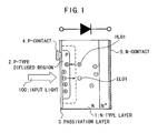
- the present invention relates to a photo diode array, and in particular, to a photo diode array whose linearity can be improved.
- a photo diode is formed by making a PN junction with a p-type region on the light-receiving surface side and an n-type region on the substrate side, and a current generated by the light incident from the photo sensitive area flows from the cathode to the anode.
- Figure 1 shows a sectional view of the configuration indicating an example of such conventional photo diodes.
- a p-type diffused region 2 is formed on one side of n-type layer 1, the substrate, n-contact 5 is formed on the opposite side of n-type layer 1, and passivation layer 3 is formed on the light-receiving surface side where p-type diffused region 2 is formed.
- a p-contact 4 connected to p-type diffused region 2 is formed by removing part of passivation layer 3 using etching or the like.
- Electrons generated in the photo diode by input light 100 incident from the photo sensitive area are accumulated in n-type layer 1, while holes are accumulated in p-type diffused region 2. Accordingly, n-type layer 1 is negatively charged and p-type diffused region 2 is positively charged. Thus, if an external circuit is connected between p-type diffused region 2 and n-type layer 1, electrons and holes flow toward the opposite layers from n-type layer 1 and p-type diffused region 2 respectively.
- an electron generated in p-type diffused region 2 shown as "EL01” in Figure 1 is accelerated towards n-type layer 1 by the electric field in the photo diode and accumulated there.
- a hole generated in n-type layer 1 shown as "HL01” in Figure 1 is accelerated towards p-type diffused region 2 and accumulated there.
- a photo diode array is composed of multiple such photo diodes arranged forming an array.
- Figure 2 shows a plan indicating an example of such a conventional photo diode array.
- Photo diodes 6a to 6e are arranged forming an array on a substrate (not shown) so that their photo sensitive area are oriented to a direction and electrodes 7a to 7e are connected to one end of the photo sensitive area of photo diodes 6a to 6e respectively.
- current values taken out may vary due to the incident positions of input light. For instance, if the input light is incident to a portion marked "P001" in Figure 2 , the distance from that portion to electrode 7e is longer compared with the case where the input light is incident to the portion marked "P002" in Figure 2 .
- a bias voltage forming a reverse bias is generally applied to the photo diode.
- a bias voltage serves to improve the frequency response and linearity, a problem exists that this causes an increase in dark current and so increases the noise, and also has the danger of breaking the photo diode.
- EP A 0 799 661 teaches electrodes which are lead-out alternately in connection with a photo diode array, however, fails to disclose two electrodes which are connected to both ends of photo sensitive area of one photodiode.
- US A 4 775 880 teaches photo conductors and comb-shaped electrodes are arranged on the surface of a device.
- JP A 03 159168 discloses plural photo diodes, which are connected to one electrode.
- the subject of the present invention is to realize a photo diode array in which linearity can be improved.
- Figure 1 shows a sectional view of the configuration indicating an example of conventional photo diodes.
- Figure 2 shows a plan indicating an example of conventional photo diode arrays.
- Figure 3 shows a plan indicating an embodiment of a photo diode array not forming part of, but necessary to understand the present invention.
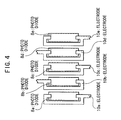
- Figure 4 shows a plan indicating the second embodiment of a photo diode array not forming part of, but necessary to understand the present invention.
- Figure 5 shows a plan indicating the third embodiment of a photo diode array based on the present invention.
- Figure 3 shows a plan indicating an embodiment of photo diode array not forming part of, but necessary to understand the present invention.
- Photo diodes 8a to 8e are arranged on a substrate (not shown) forming an array so that their photo sensitive area are oriented to a direction. Electrodes 9a to 9e are connected to one end of the photo sensitive area of photo diodes 8a to 8e respectively and also connected to the other end of the photo sensitive area of photo diodes 8a to 8e respectively by extending the electrodes between the photo sensitive area of two adjacent diodes.
- electrodes 9a to 9e connected to both ends of photo sensitive area photo diodes 8a to 8e respectively are wired on the substrate in a direction downwards in Figure 3 to be led out to the outside.
- the distance from the portion of "P101” to electrode 9e is that from the portion of "P101" to the connecting portion marked “ED01” in Figure 3 .
- the distance from the portion of "P102” to electrode 9e is that from the portion of "P102” to the connecting portion marked “ED02” in Figure 3 . That is, in both cases where the input light is incident to the portions marked "P101" and “P102” in Figure 3 , the distances to electrode 9e are the same.
- FIG. 3 shows a plan indicating the second embodiment of a photo diode array not forming part of, but necessary to understand the present invention, in which the electrode lead-out direction is modified.
- Photo diodes 8a to 8e are arranged forming an array on a substrate (not shown) so that the light-receiving surfaces face to this side. Electrodes 10a to 10e are connected to one end of the photo sensitive area of photo diodes 8a to 8e respectively as well as connected to the other ends of the photo sensitive area of photo diodes 8a to 8e respectively by extending the electrodes between adjacent photo diodes.
- electrodes 10a, 10c, and 10e connected to both ends of the photo sensitive area of photo diodes 8a, 8c, and 8e respectively are extended on the substrate towards the bottom of Figure 4 to be led out to the outside, while electrodes 10b and 10d connected to both ends of the photo sensitive area photo diodes 8b and 8d respectively are extended on the substrate towards the top of Figure 4 to be led out to the outside.
- the electrode lead-out direction is changed alternately (every other electrode).
- the method of determining the electrode lead-out direction is not limited to the above but any number of electrodes may be led out in both directions.
- the lead-out direction may be changed regularly, for example, for every two electrodes, three electrodes, etc.
- the lead-out direction may also be changed irregularly.
- the electrodes extended between adjacent photo diodes may be made transparent to secure the photo sensitive area of those portions of the photo diodes.
- Figure 5 shows a plan indicating the third embodiment of a photo diode array, this embodiment being part of the present invention and using such transparent electrodes in part of the array.
- Photo diodes 11a to 11e are arranged forming an array on a substrate (not shown) so that the light-receiving surfaces face to this side. Electrodes 12a to 12e are connected to one end of the photo sensitive area of photo diodes 11a to 11e and electrodes 14a to 14e to the other ends of photo diodes 11a to 11e respectively.
- electrodes 12a and 14a are connected to each other by transparent electrode extension 13a located between adjacent photo diodes, and electrodes 12b and 14b are connected to each other by transparent electrode extension 13b located between adjacent photo diodes.
- Electrodes 12c, 12d and 12e and electrodes 14c, 14d and 14e are connected to each other respectively by corresponding transparent electrodes 13c, 13d and 13e extended between adjacent photo diodes.
- electrodes 12a, 12c and 12e connected to one end of each photo sensitive area of photo diodes 11a, 11c and 11e respectively are wired on the substrate to lead out to the outside towards the bottom of Figure 5 .
- Electrodes 12b and 12d connected to one end of each photo sensitive area of photo diodes 11b and 11d respectively are wired on the substrate to lead out to the outside towards the top of Figure 5 .
- the light-receiving areas of the photo diodes can be increased compared with the embodiments shown in Figures 3 and 4 because these transparent electrode extensions may overlap with the photo diodes.
- electrode extensions connecting both ends of the photo sensitive area of photo diodes respectively are passed between the target photo diodes and the next photo diodes on the left side of the target photo diodes respectively.
- electrode extensions connecting both ends of the photo sensitive area of photo diodes respectively may of course be passed between the target photo diodes and the next photo diodes on the right side of the target photo diodes respectively.
- Electrodes that are led out in both directions alternately is shown.
- the electrodes may of course be led out in one direction only or alternately for every two electrodes in both directions or irregularly in both directions.
- the distance between the input light incident position and the electrodes is shortened by employing the configuration in which currents are taken out from both ends of each photo sensitive area of every photo diode.
- wiring to the electrodes becomes easy by leading out the electrodes in both directions from the photo sensitive area of photo diodes because spaces for wiring to the electrodes are secured.
Landscapes
- Light Receiving Elements (AREA)
- Facsimile Heads (AREA)
- Solid State Image Pick-Up Elements (AREA)
Claims (7)
- Fotodiodenarray mit:einer Mehrzahl von Fotodioden (11a bis 11e), die unter Bildung eines Arrays angeordnet sind;einer Mehrzahl von Elektroden (12a bis 12e, 14a bis 14e), die mit dem lichtempfindlichen Gebiet der Fotodioden (11a bis 11e) verbunden sind und Ströme entnehmen, die in den oben genannten Fotodioden (11a bis 11e) erzeugt werden;dadurch gekennzeichnet, dassjede Elektrode (12a bis 12e, 14a bis 14e) aus zwei Verbindungsabschnitten und einer Elektrodenverlängerung (13a bis 13e) gebildet ist, die die oben genannten zwei Verbindungsabschnitte verbindet;wobei die Elektrodenverlängerung (13a bis 13e) eine transparente Elektrodenverlängerung ist, die zwischen einer Fotodiode (11a bis 11e) und einer benachbarten Fotodiode (11a bis 11e) angeordnet und mit den oben genannten zwei Verbindungsabschnitten jeweils verbunden ist; undwobei jeder der zwei Verbindungsabschnitte (ED01, ED02) mit einem jeweiligen Ende des lichtempfindlichen Gebiets der Fotodiode (11a bis 11e) verbunden ist.
- Fotodiodenarray nach Anspruch 1, dadurch gekennzeichnet, das die Elektrodenverlängerungen zwischen benachbarten lichtempfindlichen Gebieten der Fotodioden (11a bis 11e) angeordnet sind.
- Fotodiodenarray nach Anspruch 2, dadurch gekennzeichnet, das die transparente Elektrode aus Indium-Zinnoxid gebildet ist.
- Fotodiodenarray nach einem der Ansprüche 1 und 2, dadurch gekennzeichnet, das es nur eine herausführende Richtung für die Elektroden (9a bis 9e) von dem lichtempfindlichen Gebiet der Fotodiode (11a bis 11e) gibt.
- Fotodiodenarray nach einem der Ansprüche 1 und 2, dadurch gekennzeichnet, das die herausführende Richtung der Elektroden (12a bis 12e) in beide Richtungen von einem Ende und dem anderen Ende des lichtempfindlichen Gebiets der Fotodioden (11a bis 11e) ist.
- Fotodiodenarray nach Anspruch 5, dadurch gekennzeichnet, das die Elektroden (12a bis 12e) herausführende Elektroden abwechselnd in beide Richtungen von beiden Enden des lichtempfindlichen Gebiets der Fotodioden (11a bis 11e) sind.
- Fotodiodenarray nach Anspruch 5, dadurch gekennzeichnet, das die Elektroden (12a bis 12e) jeweils herausführende Elektroden in der folgenden Reihenfolge sind:in einer Richtung von jedem Ende der lichtempfindlichen Gebiets der Fotodioden (11a bis 11e) undals nächstes in die andere Richtung von dem anderen Ende von einem der lichtempfindlichen Gebiete der Fotodioden (11a bis 11e).
Priority Applications (1)
| Application Number | Priority Date | Filing Date | Title |
|---|---|---|---|
| EP10173659A EP2249388A3 (de) | 1999-05-11 | 2000-05-04 | Photodiodenanordnung |
Applications Claiming Priority (2)
| Application Number | Priority Date | Filing Date | Title |
|---|---|---|---|
| JP12993399A JP4165785B2 (ja) | 1999-05-11 | 1999-05-11 | フォトダイオードアレイ |
| JP12993399 | 1999-05-11 |
Related Child Applications (1)
| Application Number | Title | Priority Date | Filing Date |
|---|---|---|---|
| EP10173659.3 Division-Into | 2010-08-23 |
Publications (3)
| Publication Number | Publication Date |
|---|---|
| EP1052697A2 EP1052697A2 (de) | 2000-11-15 |
| EP1052697A3 EP1052697A3 (de) | 2004-03-24 |
| EP1052697B1 true EP1052697B1 (de) | 2011-07-13 |
Family
ID=15022023
Family Applications (2)
| Application Number | Title | Priority Date | Filing Date |
|---|---|---|---|
| EP10173659A Withdrawn EP2249388A3 (de) | 1999-05-11 | 2000-05-04 | Photodiodenanordnung |
| EP00109551A Expired - Lifetime EP1052697B1 (de) | 1999-05-11 | 2000-05-04 | Photodiodenanordnung |
Family Applications Before (1)
| Application Number | Title | Priority Date | Filing Date |
|---|---|---|---|
| EP10173659A Withdrawn EP2249388A3 (de) | 1999-05-11 | 2000-05-04 | Photodiodenanordnung |
Country Status (4)
| Country | Link |
|---|---|
| US (1) | US6552325B1 (de) |
| EP (2) | EP2249388A3 (de) |
| JP (1) | JP4165785B2 (de) |
| CA (1) | CA2308100C (de) |
Families Citing this family (5)
| Publication number | Priority date | Publication date | Assignee | Title |
|---|---|---|---|---|
| US7702904B2 (en) | 2002-11-15 | 2010-04-20 | Nec Corporation | Key management system and multicast delivery system using the same |
| WO2007033610A1 (en) * | 2005-09-26 | 2007-03-29 | Hongkong Applied Science And Technology Research Institute Co., Ltd. | Photo-detectors and optical devices incorporating same |
| JP5271104B2 (ja) * | 2009-02-13 | 2013-08-21 | 浜松ホトニクス株式会社 | リニアイメージセンサ |
| JP5091886B2 (ja) | 2009-02-13 | 2012-12-05 | 浜松ホトニクス株式会社 | イメージセンサ |
| US12451664B2 (en) | 2019-12-20 | 2025-10-21 | Nichia Corporation | Light-receiving element and light-emitting device |
Family Cites Families (11)
| Publication number | Priority date | Publication date | Assignee | Title |
|---|---|---|---|---|
| DE3688520T2 (de) * | 1985-12-27 | 1993-09-23 | Toshiba Kawasaki Kk | Festkoerperbildsensor mit amorpher, halbleitender, photoleitender zellenmatrix. |
| US4972254A (en) * | 1987-02-24 | 1990-11-20 | Kabushiki Kaisha Toshiba | Solid state image sensors for reproducing high definition images |
| JPH03159168A (ja) * | 1989-11-16 | 1991-07-09 | Nippon Steel Corp | 完全密着型イメージセンサ |
| JPH03171667A (ja) * | 1989-11-29 | 1991-07-25 | Sharp Corp | 密着型イメージセンサ |
| US5254848A (en) * | 1991-06-21 | 1993-10-19 | Fuji Xerox Co., Ltd. | Image sensor and method of reading data out of the same having load capacitors being respectively continuously connected to common signal lines |
| JP2687831B2 (ja) * | 1992-12-04 | 1997-12-08 | 日本電気株式会社 | 受光半導体装置、その製造方法およびそれを用いた光結合装置 |
| US5397920A (en) * | 1994-03-24 | 1995-03-14 | Minnesota Mining And Manufacturing Company | Light transmissive, electrically-conductive, oxide film and methods of production |
| FR2726691B1 (fr) * | 1994-11-08 | 1997-01-24 | Thomson Csf | Photodetecteur de grande dimension et procede de realisation d'un tel photodetecteur |
| US5821567A (en) * | 1995-12-13 | 1998-10-13 | Oki Electric Industry Co., Ltd. | High-resolution light-sensing and light-emitting diode array |
| US5838054A (en) * | 1996-12-23 | 1998-11-17 | General Electric Company | Contact pads for radiation imagers |
| JP3697827B2 (ja) * | 1997-03-31 | 2005-09-21 | 株式会社島津製作所 | フラット・パネル形センサ |
-
1999
- 1999-05-11 JP JP12993399A patent/JP4165785B2/ja not_active Expired - Fee Related
-
2000
- 2000-04-28 US US09/560,758 patent/US6552325B1/en not_active Expired - Fee Related
- 2000-05-04 EP EP10173659A patent/EP2249388A3/de not_active Withdrawn
- 2000-05-04 EP EP00109551A patent/EP1052697B1/de not_active Expired - Lifetime
- 2000-05-10 CA CA002308100A patent/CA2308100C/en not_active Expired - Fee Related
Also Published As
| Publication number | Publication date |
|---|---|
| EP1052697A3 (de) | 2004-03-24 |
| EP2249388A2 (de) | 2010-11-10 |
| JP2000323743A (ja) | 2000-11-24 |
| EP1052697A2 (de) | 2000-11-15 |
| CA2308100A1 (en) | 2000-11-11 |
| EP2249388A3 (de) | 2012-08-22 |
| JP4165785B2 (ja) | 2008-10-15 |
| US20030085341A1 (en) | 2003-05-08 |
| CA2308100C (en) | 2004-11-02 |
| US6552325B1 (en) | 2003-04-22 |
Similar Documents
| Publication | Publication Date | Title |
|---|---|---|
| US11289614B2 (en) | Photoelectric conversion element and photoelectric conversion module | |
| JP7454917B2 (ja) | 光検出装置 | |
| EP4230974B1 (de) | Photodetektorvorrichtung | |
| US8350351B2 (en) | Semiconductor light receiving device | |
| US20180026145A1 (en) | Light detection device | |
| CN112352141A (zh) | 环境光探测器、探测器阵列及方法 | |
| EP1052697B1 (de) | Photodiodenanordnung | |
| JP6734644B2 (ja) | 光電変換装置 | |
| KR20210130596A (ko) | 광 센서, 광 센싱 회로 및 전자 장치 | |
| JPS6341226B2 (de) | ||
| US7777234B2 (en) | Light-receiving element and photonic semiconductor device provided therewith | |
| US12199210B2 (en) | Optical semiconductor element | |
| JP5474662B2 (ja) | 半導体受光素子 | |
| US5942749A (en) | Photodetector having means for processing optical input signals | |
| KR100884203B1 (ko) | 광차단층을 구비한 이미지센서 | |
| JPH06163977A (ja) | フォトカプラ | |
| US5216274A (en) | Image sensor | |
| US4210924A (en) | Semiconductor controlled rectifier with configured cathode to eliminate hot-spots | |
| TWI785342B (zh) | 輻射偵測裝置 | |
| JP3270874B2 (ja) | リニアセンサ | |
| KR20260051914A (ko) | 광 검출 소자 어레이 | |
| US20250123412A1 (en) | Radiation detector and radiation detector array | |
| JP2004309387A (ja) | 光学式エンコーダ | |
| JP2609608B2 (ja) | 半導体装置 | |
| JP2013016714A (ja) | 半導体受光素子、その製造方法および半導体装置 |
Legal Events
| Date | Code | Title | Description |
|---|---|---|---|
| PUAI | Public reference made under article 153(3) epc to a published international application that has entered the european phase |
Free format text: ORIGINAL CODE: 0009012 |
|
| AK | Designated contracting states |
Kind code of ref document: A2 Designated state(s): AT BE CH CY DE DK ES FI FR GB GR IE IT LI LU MC NL PT SE |
|
| AX | Request for extension of the european patent |
Free format text: AL;LT;LV;MK;RO;SI |
|
| PUAL | Search report despatched |
Free format text: ORIGINAL CODE: 0009013 |
|
| AK | Designated contracting states |
Kind code of ref document: A3 Designated state(s): AT BE CH CY DE DK ES FI FR GB GR IE IT LI LU MC NL PT SE |
|
| AX | Request for extension of the european patent |
Extension state: AL LT LV MK RO SI |
|
| 17P | Request for examination filed |
Effective date: 20040507 |
|
| AKX | Designation fees paid |
Designated state(s): DE GB |
|
| GRAP | Despatch of communication of intention to grant a patent |
Free format text: ORIGINAL CODE: EPIDOSNIGR1 |
|
| GRAC | Information related to communication of intention to grant a patent modified |
Free format text: ORIGINAL CODE: EPIDOSCIGR1 |
|
| GRAS | Grant fee paid |
Free format text: ORIGINAL CODE: EPIDOSNIGR3 |
|
| GRAA | (expected) grant |
Free format text: ORIGINAL CODE: 0009210 |
|
| AK | Designated contracting states |
Kind code of ref document: B1 Designated state(s): DE GB |
|
| REG | Reference to a national code |
Ref country code: GB Ref legal event code: FG4D |
|
| REG | Reference to a national code |
Ref country code: DE Ref legal event code: R096 Ref document number: 60046194 Country of ref document: DE Effective date: 20110901 |
|
| PLBE | No opposition filed within time limit |
Free format text: ORIGINAL CODE: 0009261 |
|
| STAA | Information on the status of an ep patent application or granted ep patent |
Free format text: STATUS: NO OPPOSITION FILED WITHIN TIME LIMIT |
|
| 26N | No opposition filed |
Effective date: 20120416 |
|
| REG | Reference to a national code |
Ref country code: DE Ref legal event code: R097 Ref document number: 60046194 Country of ref document: DE Effective date: 20120416 |
|
| PGFP | Annual fee paid to national office [announced via postgrant information from national office to epo] |
Ref country code: GB Payment date: 20140430 Year of fee payment: 15 |
|
| PGFP | Annual fee paid to national office [announced via postgrant information from national office to epo] |
Ref country code: DE Payment date: 20140430 Year of fee payment: 15 |
|
| REG | Reference to a national code |
Ref country code: DE Ref legal event code: R119 Ref document number: 60046194 Country of ref document: DE |
|
| GBPC | Gb: european patent ceased through non-payment of renewal fee |
Effective date: 20150504 |
|
| PG25 | Lapsed in a contracting state [announced via postgrant information from national office to epo] |
Ref country code: GB Free format text: LAPSE BECAUSE OF NON-PAYMENT OF DUE FEES Effective date: 20150504 Ref country code: DE Free format text: LAPSE BECAUSE OF NON-PAYMENT OF DUE FEES Effective date: 20151201 |