EP1052780A2 - Circuit intégré avec convertisseur A/N ou N/A avec isolement galvanique - Google Patents
Circuit intégré avec convertisseur A/N ou N/A avec isolement galvanique Download PDFInfo
- Publication number
- EP1052780A2 EP1052780A2 EP00109446A EP00109446A EP1052780A2 EP 1052780 A2 EP1052780 A2 EP 1052780A2 EP 00109446 A EP00109446 A EP 00109446A EP 00109446 A EP00109446 A EP 00109446A EP 1052780 A2 EP1052780 A2 EP 1052780A2
- Authority
- EP
- European Patent Office
- Prior art keywords
- integrated circuit
- digital
- converter
- analog
- output
- Prior art date
- Legal status (The legal status is an assumption and is not a legal conclusion. Google has not performed a legal analysis and makes no representation as to the accuracy of the status listed.)
- Withdrawn
Links
Images
Classifications
-
- H—ELECTRICITY
- H03—ELECTRONIC CIRCUITRY
- H03M—CODING; DECODING; CODE CONVERSION IN GENERAL
- H03M3/00—Conversion of analogue values to or from differential modulation
- H03M3/30—Delta-sigma modulation
- H03M3/32—Delta-sigma modulation with special provisions or arrangements for power saving, e.g. by allowing a sleep mode, using lower supply voltage for downstream stages, using multiple clock domains, by selectively turning on stages when needed
-
- H—ELECTRICITY
- H03—ELECTRONIC CIRCUITRY
- H03M—CODING; DECODING; CODE CONVERSION IN GENERAL
- H03M1/00—Analogue/digital conversion; Digital/analogue conversion
- H03M1/002—Provisions or arrangements for saving power, e.g. by allowing a sleep mode, using lower supply voltage for downstream stages, using multiple clock domains or by selectively turning on stages when needed
-
- H—ELECTRICITY
- H03—ELECTRONIC CIRCUITRY
- H03M—CODING; DECODING; CODE CONVERSION IN GENERAL
- H03M1/00—Analogue/digital conversion; Digital/analogue conversion
- H03M1/06—Continuously compensating for, or preventing, undesired influence of physical parameters
- H03M1/08—Continuously compensating for, or preventing, undesired influence of physical parameters of noise
- H03M1/0827—Continuously compensating for, or preventing, undesired influence of physical parameters of noise of electromagnetic or electrostatic field noise, e.g. preventing crosstalk by shielding or optical isolation
-
- H—ELECTRICITY
- H03—ELECTRONIC CIRCUITRY
- H03M—CODING; DECODING; CODE CONVERSION IN GENERAL
- H03M1/00—Analogue/digital conversion; Digital/analogue conversion
- H03M1/12—Analogue/digital converters
-
- H—ELECTRICITY
- H03—ELECTRONIC CIRCUITRY
- H03M—CODING; DECODING; CODE CONVERSION IN GENERAL
- H03M1/00—Analogue/digital conversion; Digital/analogue conversion
- H03M1/66—Digital/analogue converters
-
- H—ELECTRICITY
- H03—ELECTRONIC CIRCUITRY
- H03M—CODING; DECODING; CODE CONVERSION IN GENERAL
- H03M3/00—Conversion of analogue values to or from differential modulation
- H03M3/30—Delta-sigma modulation
- H03M3/322—Continuously compensating for, or preventing, undesired influence of physical parameters
- H03M3/368—Continuously compensating for, or preventing, undesired influence of physical parameters of noise other than the quantisation noise already being shaped inherently by delta-sigma modulators
-
- H—ELECTRICITY
- H03—ELECTRONIC CIRCUITRY
- H03M—CODING; DECODING; CODE CONVERSION IN GENERAL
- H03M3/00—Conversion of analogue values to or from differential modulation
- H03M3/30—Delta-sigma modulation
- H03M3/458—Analogue/digital converters using delta-sigma modulation as an intermediate step
-
- H—ELECTRICITY
- H03—ELECTRONIC CIRCUITRY
- H03M—CODING; DECODING; CODE CONVERSION IN GENERAL
- H03M3/00—Conversion of analogue values to or from differential modulation
- H03M3/30—Delta-sigma modulation
- H03M3/50—Digital/analogue converters using delta-sigma modulation as an intermediate step
Definitions
- the invention relates to an integrated circuit, which an analog / digital converter or a digital / analog converter as well as an analog and an associated with it contains digital signal path.
- a / D converters and D / A converters are already known.
- An A / D converter digitizes the samples of an existing time function and delivers them Input signals for a digital processor.
- a D / A converter works reciprocally to the A / D converter. It converts a coded set of digital values into a changing analog voltage.
- tracking errors and Trembling errors occur that affect the accuracy of the conversion.
- the effects of various electrical or mechanical sources of error in D / A converters are attempted to be minimized by selecting precision components, using precision power supplies, reducing the operating temperature range, etc.
- a / D converters and D / A converters are also from the book published by Springer Verlag in 1990 Semiconductor circuit technology "from U. Tietze and Ch. Schenk, pages 751 to 790.
- a converter of this type can be implemented using the parallel method, the weighing method and the counting method.
- the converters mentioned are generally offered as integrated circuits , for example C-MOS circuits.
- An integrated data transmission circuit is already known from DE-197 18 420 A1 with electrical isolation between input and Output circuit known. These are binary on the input side Input signals supplied using a arranged within the integrated data transmission circuit magnetosensitive coupling element transmitted and on Output of the integrated data transmission circuit as a binary Output signals are made available.
- the object of the invention is one in the form of a integrated circuit realized analog / digital converter or digital / analog converter in such a way that the overall circuit within which it is arranged one has reduced power consumption.
- an A / D converter implemented as an integrated circuit or D / A converter with the features according to the invention the integration of the device for electrical isolation in the digital provided within the integrated circuit Signal path consumes significantly less energy than one Transducers with upstream or downstream, by means of discrete Components of potential isolation. Furthermore needs a converter according to the invention in its implementation less area, which is a miniaturization of A / D or D / A converters favored. Furthermore, such Converter achieved higher data rates. Such are also To implement transducers also cheaper than known ones Converter.
- the invention creates a new class of Components made available which are the functions an A / D or D / A converter and a non-contact data transmission circuit unite in itself. This principle can be applied to all common A / D and D / A converters.
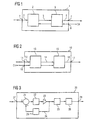
- Figure 1 shows a block diagram of an integrated Circuit 1, which contains an analog / digital converter 2.
- the input 4 of the integrated circuit 1 is the Analog signal to be converted, which is then fed from the input 4 of the integrated circuit 1 from an analog Signal path 3 is supplied to the analog / digital converter 2.
- This provides a digital value at its output digital signal available, which via a digital Signal path 5, 6 to the output 7 of the integrated Circuit 1 is forwarded.
- the device for electrical isolation has a conductor loop on the input side, via which the signal present in digital form is carried becomes.
- This digital signal is in the surrounding area the conductor loop generates a magnetic field, which is in Dependence on the digital signal changes.
- This changing Magnetic field is detected by a magnetic field detector, which is separated from the conductor loop by an insulator is, but in the area of the mentioned magnetic field located.
- the signal detected by the magnetic field detector is as a galvanically separated digital signal from the input side available at output 7 of integrated circuit 1 posed.
- a digital Clock signal required. This becomes the integrated circuit supplied via an input 8 and via the device 9 for Electrical isolation passed on to the analog / digital converter 2. This creates within the device 9 for Electrical isolation two transmission channels, one of which one data transmission channel and the other a clock transmission channel is.
- the magnetic field detector of the device 9 for potential isolation can be realized in the form of a Hall element. Farther it can also be the case with the magnetic field detector mentioned an AMR sensor (anisotropic magnetic resistance), which points to a changing magnetic field with a Change in resistance reacts. Such AMR sensors have a permalloy layer.
- GMR sensor giant magnetic resistance
- Such sensors have a Combination of three layers, two of which are soft magnetic are and is hard magnetic.
- TMR sensor tunnel magnetic resistance
- FIG. 2 shows a block diagram of an integrated Circuit 10, which a digital / analog converter 15th contains.
- the input 11 of the integrated circuit is the digital signal to be converted, which is then from the Input 11 of the integrated circuit 10 via a digital Signal path 12, 14 supplied to the digital / analog converter 15 becomes.
- This provides an analog signal at its output available via an analog signal path 16 forwarded to the output 17 of the integrated circuit 10 becomes.
- the digital signal path 12 there is a device 13 for Potential isolation is provided, which consequently the digital / analog converter 15 is connected upstream.
- the device 13 for potential isolation itself is constructed just like that Device 9 described above in connection with FIG. 1 for electrical isolation.
- the digital clock signal required in the digital / analog converter 15 is generated outside of the integrated circuit 10 and this supplied via the terminal 18.
- the integrated Circuit 10 passes the digital clock signal through the device 13 for electrical isolation as electrically isolated digital Clock signal to the digital / analog converter 15. This arise within the device 13 for electrical isolation two transmission channels, one of which is a data transmission channel and the other is a clock transmission channel.
- Figure 3 shows a block diagram of an integrated Circuit 20, which as an analog / digital converter Contains sigma-delta converter. This creates a 1-bit data stream whose logical level depends on whether that signal to be converted larger or smaller than one due to this Comparative signal obtained and then integrated is.
- the integrated circuit 20 shown is via the input 27 an analog input signal is supplied. This will from the input 27 to the inside of the integrated circuit 20th arranged sigma-delta converter forwarded. This points a subtraction level 21, in which the over a Feedback path 24 returned signal, which in a Digital / analog converter 29 converted back into an analog signal is subtracted from the input signal.
- the output signal the subtractor 21 is in an integrator 22 integrated and supplied by this from the comparator 23.
- the digital signal is the one already mentioned above 1-bit data stream available.
- this is in the feedback path 24 subjected to a digital / analog conversion and as a subtrahend the subtracting stage 21 supplied.
- the 1-bit data stream is sent to a device 25 led to electrical isolation.
- a device 25 led to electrical isolation.
- the digital output signal of the device 25 for electrical isolation is via a digital filter 26, which is also part of the integrated circuit 20 is to the output 28 of the integrated circuit 20 forwarded.
- This embodiment also takes place in one and the same integrated circuit both an analog / digital conversion as well as a potential separation. This leads to Saving compared to known analog / digital converters of electricity, space and implementation costs and enables a higher data rate.
Landscapes
- Engineering & Computer Science (AREA)
- Theoretical Computer Science (AREA)
- Analogue/Digital Conversion (AREA)
- Compression, Expansion, Code Conversion, And Decoders (AREA)
- Semiconductor Integrated Circuits (AREA)
Applications Claiming Priority (2)
| Application Number | Priority Date | Filing Date | Title |
|---|---|---|---|
| DE1999122127 DE19922127C2 (de) | 1999-05-12 | 1999-05-12 | Integrierter Schaltkreis mit einem A/D- oder D/A-Wandler mit galvanischer Trennung |
| DE19922127 | 1999-05-12 |
Publications (2)
| Publication Number | Publication Date |
|---|---|
| EP1052780A2 true EP1052780A2 (fr) | 2000-11-15 |
| EP1052780A3 EP1052780A3 (fr) | 2003-08-06 |
Family
ID=7907988
Family Applications (1)
| Application Number | Title | Priority Date | Filing Date |
|---|---|---|---|
| EP00109446A Withdrawn EP1052780A3 (fr) | 1999-05-12 | 2000-05-03 | Circuit intégré avec convertisseur A/N ou N/A avec isolement galvanique |
Country Status (2)
| Country | Link |
|---|---|
| EP (1) | EP1052780A3 (fr) |
| DE (1) | DE19922127C2 (fr) |
Cited By (4)
| Publication number | Priority date | Publication date | Assignee | Title |
|---|---|---|---|---|
| FR2818018A1 (fr) * | 2000-12-12 | 2002-06-14 | Thomson Csf | Antenne rayonnante a isolation galvanique |
| EP2169830A2 (fr) | 2008-09-26 | 2010-03-31 | Siemens Aktiengesellschaft | Dispositif de conversion d'un signal analogique en un signal numérique |
| US8189693B2 (en) | 2002-09-18 | 2012-05-29 | Infineon Technologies Ag | Digital signal transfer method and apparatus |
| EP4262161A1 (fr) | 2022-04-13 | 2023-10-18 | Abb Schweiz Ag | Module d'entrée binaire universel |
Families Citing this family (11)
| Publication number | Priority date | Publication date | Assignee | Title |
|---|---|---|---|---|
| US6873065B2 (en) | 1997-10-23 | 2005-03-29 | Analog Devices, Inc. | Non-optical signal isolator |
| US20030042571A1 (en) | 1997-10-23 | 2003-03-06 | Baoxing Chen | Chip-scale coils and isolators based thereon |
| US6262600B1 (en) | 2000-02-14 | 2001-07-17 | Analog Devices, Inc. | Isolator for transmitting logic signals across an isolation barrier |
| DE10159607B4 (de) * | 2001-03-09 | 2010-11-18 | Siemens Ag | Analog/Digital-Signalwandlereinrichtung mit galvanischer Trennung in ihrem Singalübertragungsweg |
| WO2004100473A2 (fr) | 2003-04-30 | 2004-11-18 | Analog Devices, Inc. | Isolateurs de signal utilisant des micro-transformateurs |
| US7719305B2 (en) | 2006-07-06 | 2010-05-18 | Analog Devices, Inc. | Signal isolator using micro-transformers |
| US9293997B2 (en) | 2013-03-14 | 2016-03-22 | Analog Devices Global | Isolated error amplifier for isolated power supplies |
| US10270630B2 (en) | 2014-09-15 | 2019-04-23 | Analog Devices, Inc. | Demodulation of on-off-key modulated signals in signal isolator systems |
| US10536309B2 (en) | 2014-09-15 | 2020-01-14 | Analog Devices, Inc. | Demodulation of on-off-key modulated signals in signal isolator systems |
| US9660848B2 (en) | 2014-09-15 | 2017-05-23 | Analog Devices Global | Methods and structures to generate on/off keyed carrier signals for signal isolators |
| US9998301B2 (en) | 2014-11-03 | 2018-06-12 | Analog Devices, Inc. | Signal isolator system with protection for common mode transients |
Family Cites Families (6)
| Publication number | Priority date | Publication date | Assignee | Title |
|---|---|---|---|---|
| DE3726582C2 (de) * | 1987-08-10 | 1995-06-01 | Siemens Ag | Verfahren und Vorrichtung zur Wandlung von Eingangsgrößen, insbesondere zur simultanen Analog/Digitalumsetzung |
| DE4205241C2 (de) * | 1992-02-21 | 1997-12-18 | Itt Ind Gmbh Deutsche | Potentialfreie Datenübertragungseinrichtung |
| DE4324865A1 (de) * | 1993-07-23 | 1995-01-26 | Gore W L & Ass Gmbh | Leckage-Erkennungssystem |
| JPH0758638A (ja) * | 1993-08-11 | 1995-03-03 | Yokogawa Electric Corp | A/d変換装置 |
| JPH0897722A (ja) * | 1994-09-29 | 1996-04-12 | Hakko Denki Kk | シーケンサ用のda変換増設ユニット |
| DE19718420A1 (de) * | 1997-04-30 | 1998-11-12 | Siemens Ag | Integrierte Datenübertragungsschaltung mit Potentialtrennung zwischen Ein- und Ausgangsschaltkreis |
-
1999
- 1999-05-12 DE DE1999122127 patent/DE19922127C2/de not_active Expired - Fee Related
-
2000
- 2000-05-03 EP EP00109446A patent/EP1052780A3/fr not_active Withdrawn
Cited By (6)
| Publication number | Priority date | Publication date | Assignee | Title |
|---|---|---|---|---|
| FR2818018A1 (fr) * | 2000-12-12 | 2002-06-14 | Thomson Csf | Antenne rayonnante a isolation galvanique |
| EP1215754A1 (fr) * | 2000-12-12 | 2002-06-19 | Thales | Antenne rayonnante à isolation galvanique |
| US8189693B2 (en) | 2002-09-18 | 2012-05-29 | Infineon Technologies Ag | Digital signal transfer method and apparatus |
| US10419251B2 (en) | 2002-09-18 | 2019-09-17 | Infineon Technologies | Digital signal transfer using integrated transformers with electrical isolation |
| EP2169830A2 (fr) | 2008-09-26 | 2010-03-31 | Siemens Aktiengesellschaft | Dispositif de conversion d'un signal analogique en un signal numérique |
| EP4262161A1 (fr) | 2022-04-13 | 2023-10-18 | Abb Schweiz Ag | Module d'entrée binaire universel |
Also Published As
| Publication number | Publication date |
|---|---|
| DE19922127C2 (de) | 2002-05-29 |
| DE19922127A1 (de) | 2000-11-23 |
| EP1052780A3 (fr) | 2003-08-06 |
Similar Documents
| Publication | Publication Date | Title |
|---|---|---|
| DE19922127C2 (de) | Integrierter Schaltkreis mit einem A/D- oder D/A-Wandler mit galvanischer Trennung | |
| DE112016002487B4 (de) | Unterdrücken von Signalübertragungsfunktionsspitzen bei einem vorwärtsgekoppelten Delta-Sigma-Wandler | |
| DE69431721T2 (de) | Elektrische ladungsübertragungsanordnung | |
| DE69330198T2 (de) | Analog Digitalwandler | |
| DE102017206177B4 (de) | Betriebsverfahren für einen Überabtastung-Datenwandler | |
| EP1959570B1 (fr) | Détecteur d'approximation inductif | |
| DE202015009602U1 (de) | LC-Gitter-Verzögerungsleitung für schnelle ADW-Anwendungen | |
| WO2006125639A1 (fr) | Circuit de mesure de capacite | |
| EP0457749B1 (fr) | Convertisseur analogique-numérique à équilibrage de charge, de haute précision | |
| DE202016009095U1 (de) | Dither-Einspeisung für zeitkontinuierliche MASH-ADC | |
| DE112009000503T5 (de) | Linearer Sensor mit zwei Anschlüssen | |
| DE102019219882B4 (de) | Strom-digital-präzisionswandler | |
| DE102023116429A1 (de) | Zeitkontinuierlicher Sigma-Delta-Analog/Digital-Wandler | |
| DE102022119660A1 (de) | Rauscharme hochgenaue sigle-ended-eingangsstufe für einen zetkontinuierlichen sigma/delta-analog/digital-umsetzer (ctsd-adc) | |
| DE102021132516A1 (de) | Verfahren, vorrichtungen und systeme zur induktiven abtastung | |
| DE102016110968A1 (de) | Sensor | |
| DE102021102068B4 (de) | Vorrichtung mit einer kapazitiven Abtaststruktur, Verfahren zur Rauschreduzierung in einer Abtaststruktur, Vorrichtung mit einer Abtaststruktur, Vorrichtung, die zur Unterdrückung oder zum Ausgleich von skaliertem thermischen Rauschen in einer Umsetzphase aus einer Aufnahme des skalierten thermischen Rauschens in einer Erfassungsphase eingerichtet ist, Verfahren zur Unterdrückung oder zum Ausgleich von skaliertem thermischen Rauschen | |
| DE102008052838B4 (de) | Abtastfehlerverringerung bei PWM-MASH-Wandlern | |
| DE102015117109B4 (de) | Digital gesteuerte Ausgangsamplitude eines Analogsensorsignals | |
| EP1300951B1 (fr) | Convertisseur analogique-numérique du type delta-sigma | |
| DE102008062607A1 (de) | Stromzellenschaltung in einem Digital-Analog-Umsetzer | |
| DE102009006546B4 (de) | Schaltungsanordnung und Verfahren zum Bereitstellen eines aufbereiteten Messsignals | |
| DE10050706C2 (de) | Schaltungsanordnung zur Umwandlung eines Eingangsstromsignals in ein entsprechendes digitales Ausgangssignal | |
| DE102005061207A1 (de) | Schaltungsanordnung zur Energieversorgung und Verfahren | |
| DE102004038370B4 (de) | Adaptive Regelvorrichtung, Verwendung der Regelvorrichtung, Sensor mit einer derartigen Regelvorrichtung und adaptives Verfahren zur Selbstkompensation von Störsignalen eines Sensors |
Legal Events
| Date | Code | Title | Description |
|---|---|---|---|
| PUAI | Public reference made under article 153(3) epc to a published international application that has entered the european phase |
Free format text: ORIGINAL CODE: 0009012 |
|
| AK | Designated contracting states |
Kind code of ref document: A2 Designated state(s): AT BE CH CY DE DK ES FI FR GB GR IE IT LI LU MC NL PT SE |
|
| AX | Request for extension of the european patent |
Free format text: AL;LT;LV;MK;RO;SI |
|
| PUAL | Search report despatched |
Free format text: ORIGINAL CODE: 0009013 |
|
| AK | Designated contracting states |
Designated state(s): AT BE CH CY DE DK ES FI FR GB GR IE IT LI LU MC NL PT SE |
|
| AX | Request for extension of the european patent |
Extension state: AL LT LV MK RO SI |
|
| 17P | Request for examination filed |
Effective date: 20031103 |
|
| 17Q | First examination report despatched |
Effective date: 20040126 |
|
| AKX | Designation fees paid |
Designated state(s): AT CH DE ES FR GB LI |
|
| STAA | Information on the status of an ep patent application or granted ep patent |
Free format text: STATUS: THE APPLICATION HAS BEEN WITHDRAWN |
|
| 18W | Application withdrawn |
Effective date: 20050209 |