EP1054296A2 - Verfahren zur Herstellung feiner Strukturen - Google Patents
Verfahren zur Herstellung feiner Strukturen Download PDFInfo
- Publication number
- EP1054296A2 EP1054296A2 EP00109254A EP00109254A EP1054296A2 EP 1054296 A2 EP1054296 A2 EP 1054296A2 EP 00109254 A EP00109254 A EP 00109254A EP 00109254 A EP00109254 A EP 00109254A EP 1054296 A2 EP1054296 A2 EP 1054296A2
- Authority
- EP
- European Patent Office
- Prior art keywords
- resist layer
- pattern forming
- forming method
- fine pattern
- resist
- Prior art date
- Legal status (The legal status is an assumption and is not a legal conclusion. Google has not performed a legal analysis and makes no representation as to the accuracy of the status listed.)
- Ceased
Links
- 238000000034 method Methods 0.000 title claims abstract description 45
- 239000000463 material Substances 0.000 claims abstract description 49
- 239000000758 substrate Substances 0.000 claims abstract description 32
- 239000002253 acid Substances 0.000 claims description 41
- 150000001875 compounds Chemical class 0.000 claims description 36
- 229920000642 polymer Polymers 0.000 claims description 27
- 229920001296 polysiloxane Polymers 0.000 claims description 25
- 239000003513 alkali Substances 0.000 claims description 21
- 230000007261 regionalization Effects 0.000 claims description 18
- 230000005855 radiation Effects 0.000 claims description 17
- 230000003287 optical effect Effects 0.000 claims description 12
- 238000006116 polymerization reaction Methods 0.000 claims description 12
- XUIMIQQOPSSXEZ-UHFFFAOYSA-N Silicon Chemical group [Si] XUIMIQQOPSSXEZ-UHFFFAOYSA-N 0.000 claims description 10
- 238000001312 dry etching Methods 0.000 claims description 10
- -1 naphthoquinone diazide compound Chemical class 0.000 claims description 10
- 230000003247 decreasing effect Effects 0.000 claims description 8
- 230000018109 developmental process Effects 0.000 claims description 8
- 239000000523 sample Substances 0.000 claims description 8
- 150000001336 alkenes Chemical class 0.000 claims description 7
- JRZJOMJEPLMPRA-UHFFFAOYSA-N olefin Natural products CCCCCCCC=C JRZJOMJEPLMPRA-UHFFFAOYSA-N 0.000 claims description 7
- 239000002904 solvent Substances 0.000 claims description 7
- 230000000977 initiatory effect Effects 0.000 claims description 6
- QVGXLLKOCUKJST-UHFFFAOYSA-N atomic oxygen Chemical compound [O] QVGXLLKOCUKJST-UHFFFAOYSA-N 0.000 claims description 5
- 229910052760 oxygen Inorganic materials 0.000 claims description 5
- 239000001301 oxygen Substances 0.000 claims description 5
- 125000000524 functional group Chemical group 0.000 claims description 4
- 230000035699 permeability Effects 0.000 claims description 4
- 239000007787 solid Substances 0.000 claims description 3
- 238000007664 blowing Methods 0.000 claims description 2
- 238000005530 etching Methods 0.000 abstract description 4
- 239000002184 metal Substances 0.000 abstract description 3
- 229910052751 metal Inorganic materials 0.000 abstract description 3
- 239000011521 glass Substances 0.000 abstract description 2
- 239000007921 spray Substances 0.000 abstract description 2
- 238000007740 vapor deposition Methods 0.000 abstract description 2
- 125000001424 substituent group Chemical group 0.000 description 25
- 125000000217 alkyl group Chemical group 0.000 description 21
- 239000000243 solution Substances 0.000 description 18
- 125000004435 hydrogen atom Chemical group [H]* 0.000 description 14
- 125000003710 aryl alkyl group Chemical group 0.000 description 12
- 125000000753 cycloalkyl group Chemical group 0.000 description 11
- 125000005843 halogen group Chemical group 0.000 description 10
- 238000001459 lithography Methods 0.000 description 9
- 125000003545 alkoxy group Chemical group 0.000 description 8
- 125000003118 aryl group Chemical group 0.000 description 7
- 125000003636 chemical group Chemical group 0.000 description 7
- 125000004432 carbon atom Chemical group C* 0.000 description 5
- 238000005516 engineering process Methods 0.000 description 5
- 230000003252 repetitive effect Effects 0.000 description 5
- 229920005989 resin Polymers 0.000 description 5
- 239000011347 resin Substances 0.000 description 5
- 229910052710 silicon Inorganic materials 0.000 description 5
- 239000010703 silicon Substances 0.000 description 5
- PPBRXRYQALVLMV-UHFFFAOYSA-N Styrene Chemical compound C=CC1=CC=CC=C1 PPBRXRYQALVLMV-UHFFFAOYSA-N 0.000 description 4
- 125000002252 acyl group Chemical group 0.000 description 4
- 125000002947 alkylene group Chemical group 0.000 description 4
- 125000003178 carboxy group Chemical group [H]OC(*)=O 0.000 description 4
- 238000007687 exposure technique Methods 0.000 description 4
- WSFSSNUMVMOOMR-UHFFFAOYSA-N Formaldehyde Chemical compound O=C WSFSSNUMVMOOMR-UHFFFAOYSA-N 0.000 description 3
- 125000003342 alkenyl group Chemical group 0.000 description 3
- 230000015572 biosynthetic process Effects 0.000 description 3
- 125000002993 cycloalkylene group Chemical group 0.000 description 3
- 150000002430 hydrocarbons Chemical group 0.000 description 3
- 125000002887 hydroxy group Chemical group [H]O* 0.000 description 3
- 239000003999 initiator Substances 0.000 description 3
- 238000004519 manufacturing process Methods 0.000 description 3
- 239000000203 mixture Substances 0.000 description 3
- 229920003986 novolac Polymers 0.000 description 3
- 238000000206 photolithography Methods 0.000 description 3
- 229920002554 vinyl polymer Polymers 0.000 description 3
- VYPSYNLAJGMNEJ-UHFFFAOYSA-N Silicium dioxide Chemical compound O=[Si]=O VYPSYNLAJGMNEJ-UHFFFAOYSA-N 0.000 description 2
- 238000001015 X-ray lithography Methods 0.000 description 2
- 125000001931 aliphatic group Chemical group 0.000 description 2
- 239000012670 alkaline solution Substances 0.000 description 2
- 125000005428 anthryl group Chemical group [H]C1=C([H])C([H])=C2C([H])=C3C(*)=C([H])C([H])=C([H])C3=C([H])C2=C1[H] 0.000 description 2
- 125000002029 aromatic hydrocarbon group Chemical group 0.000 description 2
- 239000003795 chemical substances by application Substances 0.000 description 2
- 239000003431 cross linking reagent Substances 0.000 description 2
- 238000010894 electron beam technology Methods 0.000 description 2
- 239000007789 gas Substances 0.000 description 2
- VKYKSIONXSXAKP-UHFFFAOYSA-N hexamethylenetetramine Chemical compound C1N(C2)CN3CN1CN2C3 VKYKSIONXSXAKP-UHFFFAOYSA-N 0.000 description 2
- 125000001624 naphthyl group Chemical group 0.000 description 2
- 125000001997 phenyl group Chemical group [H]C1=C([H])C([H])=C(*)C([H])=C1[H] 0.000 description 2
- 229920000734 polysilsesquioxane polymer Polymers 0.000 description 2
- 230000000644 propagated effect Effects 0.000 description 2
- 239000004065 semiconductor Substances 0.000 description 2
- 125000004469 siloxy group Chemical group [SiH3]O* 0.000 description 2
- 239000000126 substance Substances 0.000 description 2
- GZVHEAJQGPRDLQ-UHFFFAOYSA-N 6-phenyl-1,3,5-triazine-2,4-diamine Chemical compound NC1=NC(N)=NC(C=2C=CC=CC=2)=N1 GZVHEAJQGPRDLQ-UHFFFAOYSA-N 0.000 description 1
- 239000004593 Epoxy Substances 0.000 description 1
- 229910001218 Gallium arsenide Inorganic materials 0.000 description 1
- 229920000877 Melamine resin Polymers 0.000 description 1
- 230000002378 acidificating effect Effects 0.000 description 1
- 125000004442 acylamino group Chemical group 0.000 description 1
- 239000000654 additive Substances 0.000 description 1
- 230000000996 additive effect Effects 0.000 description 1
- 150000001299 aldehydes Chemical class 0.000 description 1
- 125000004453 alkoxycarbonyl group Chemical group 0.000 description 1
- 125000005160 aryl oxy alkyl group Chemical group 0.000 description 1
- 125000000732 arylene group Chemical group 0.000 description 1
- 238000004380 ashing Methods 0.000 description 1
- 238000009835 boiling Methods 0.000 description 1
- 238000010538 cationic polymerization reaction Methods 0.000 description 1
- 229910052681 coesite Inorganic materials 0.000 description 1
- 238000004040 coloring Methods 0.000 description 1
- 229910052906 cristobalite Inorganic materials 0.000 description 1
- 125000001316 cycloalkyl alkyl group Chemical group 0.000 description 1
- 238000000609 electron-beam lithography Methods 0.000 description 1
- 239000012530 fluid Substances 0.000 description 1
- 238000010438 heat treatment Methods 0.000 description 1
- 239000004312 hexamethylene tetramine Substances 0.000 description 1
- 235000010299 hexamethylene tetramine Nutrition 0.000 description 1
- 239000011261 inert gas Substances 0.000 description 1
- 238000009413 insulation Methods 0.000 description 1
- 150000002500 ions Chemical class 0.000 description 1
- JDSHMPZPIAZGSV-UHFFFAOYSA-N melamine Chemical compound NC1=NC(N)=NC(N)=N1 JDSHMPZPIAZGSV-UHFFFAOYSA-N 0.000 description 1
- 239000000178 monomer Substances 0.000 description 1
- 150000001451 organic peroxides Chemical class 0.000 description 1
- 239000003960 organic solvent Substances 0.000 description 1
- 239000010815 organic waste Substances 0.000 description 1
- 238000000059 patterning Methods 0.000 description 1
- 229920002120 photoresistant polymer Polymers 0.000 description 1
- 229920003023 plastic Polymers 0.000 description 1
- 239000004033 plastic Substances 0.000 description 1
- 239000003505 polymerization initiator Substances 0.000 description 1
- 238000010926 purge Methods 0.000 description 1
- 238000010526 radical polymerization reaction Methods 0.000 description 1
- 230000035945 sensitivity Effects 0.000 description 1
- 239000000377 silicon dioxide Substances 0.000 description 1
- 125000003808 silyl group Chemical group [H][Si]([H])([H])[*] 0.000 description 1
- 229910052682 stishovite Inorganic materials 0.000 description 1
- 230000008961 swelling Effects 0.000 description 1
- 238000012719 thermal polymerization Methods 0.000 description 1
- 229910052905 tridymite Inorganic materials 0.000 description 1
- XLYOFNOQVPJJNP-UHFFFAOYSA-N water Substances O XLYOFNOQVPJJNP-UHFFFAOYSA-N 0.000 description 1
Images


Classifications
-
- G—PHYSICS
- G03—PHOTOGRAPHY; CINEMATOGRAPHY; ANALOGOUS TECHNIQUES USING WAVES OTHER THAN OPTICAL WAVES; ELECTROGRAPHY; HOLOGRAPHY
- G03F—PHOTOMECHANICAL PRODUCTION OF TEXTURED OR PATTERNED SURFACES, e.g. FOR PRINTING, FOR PROCESSING OF SEMICONDUCTOR DEVICES; MATERIALS THEREFOR; ORIGINALS THEREFOR; APPARATUS SPECIALLY ADAPTED THEREFOR
- G03F7/00—Photomechanical, e.g. photolithographic, production of textured or patterned surfaces, e.g. printing surfaces; Materials therefor, e.g. comprising photoresists; Apparatus specially adapted therefor
- G03F7/004—Photosensitive materials
- G03F7/09—Photosensitive materials characterised by structural details, e.g. supports, auxiliary layers
- G03F7/095—Photosensitive materials characterised by structural details, e.g. supports, auxiliary layers having more than one photosensitive layer
-
- G—PHYSICS
- G03—PHOTOGRAPHY; CINEMATOGRAPHY; ANALOGOUS TECHNIQUES USING WAVES OTHER THAN OPTICAL WAVES; ELECTROGRAPHY; HOLOGRAPHY
- G03F—PHOTOMECHANICAL PRODUCTION OF TEXTURED OR PATTERNED SURFACES, e.g. FOR PRINTING, FOR PROCESSING OF SEMICONDUCTOR DEVICES; MATERIALS THEREFOR; ORIGINALS THEREFOR; APPARATUS SPECIALLY ADAPTED THEREFOR
- G03F7/00—Photomechanical, e.g. photolithographic, production of textured or patterned surfaces, e.g. printing surfaces; Materials therefor, e.g. comprising photoresists; Apparatus specially adapted therefor
- G03F7/004—Photosensitive materials
- G03F7/075—Silicon-containing compounds
- G03F7/0757—Macromolecular compounds containing Si-O, Si-C or Si-N bonds
Definitions
- the present invention relates to a fine pattern forming method, and particularly to a method which forms a fine pattern on a substrate by photolithography using near field light.
- the evolution of photolithography technology has been supported particularly by the advance of reduced projection exposure technology and resist technology.
- RP k 1 ⁇ /NA
- DOP k 2 ⁇ /NA 2 .
- NA the numerical aperture of the projection lens
- the exposure wavelength ⁇ has been shortened from that for the g-line (436 nm) to that for the i-line (365 nm), and at present, the excimer laser (248 nm, 193 nm) has become the most popular.
- the diffraction limit for light provides the limit of resolution, and it is generally accepted that, if an F2 excimer laser with a wavelength of 248 nm is used, a fine pattern of 100 nm in line width is the limit of lithography using a lens series optical system. If it is attempted to provide a resolution in the order of less than 100 nm, electron beam or X-ray (particularly SOR light, i.e., synchrotron orbital radiation) lithography technology must be used.
- Electron beam lithography can control the formation of a pattern in the order of nanometers with high accuracy, providing a significantly greater depth of focus than that for the optical system.
- it offers an advantage that it can directly draw a figure on the wafer without a mask, but because the throughput is low, and the cost is high, it has a drawback that it is far from suited to volume production.
- X-ray lithography can provide an approx. one digit higher resolution and accuracy than those for the excimer laser lithography either when full-scale exposure is carried out with a 1-to-1 mask or when a reflection type image formation optical system is used for exposure.
- X-ray lithography presents problems that the mask is difficult to prepare, the feasibility is low, and the cost is high due to the device.
- the near field light has a propagation depth of as small as several tens of nm (therefore, the word “effused” is used in place of "propagated", and in the drawings, the near field light is depicted as if it were a drop of water hanging from a faucet). It is impossible to expose a thick-film resist having a thickness as large as 1000 nm, and a problem where it is difficult to form a resist pattern with a high aspect ratio is presented.
- the line width and the line height for the resist are "a” and "b”, respectively, the aspect ratio is expressed as b/a, and it can be said that, for a given resist thickness, the higher the aspect ratio, the finer the pattern will be.
- the fine pattern forming method according to the present invention is a fine pattern forming method in which a first resist layer capable of being removed by dry etching, and a photosensitive second resist layer having a resistance to dry etching with which only the irradiated portion or only the non-irradiated portion is made soluble in a developing solvent are stacked together in this order for creating a recording material, and by means for generating near field light on the projected light, the near field light is projected onto the second resist layer of the recording material in the form of a desired pattern. Thereafter, by processing the second resist layer for development, a pattern is formed in the second resist layer, and by using the pattern as a mask, the first resist layer is dry-etched to form a pattern on the substrate of the recording material.
- the above-mentioned second resist layer preferably has a film thickness of 100 nm or less.
- the fine pattern forming method according to the present invention preferably uses a recording material which provides antireflection means against the projected light on the substrate.
- the antireflection means is preferably an antireflection film formed between the substrate and the first resist layer, or an antireflection film formed between the first resist layer and the second resist layer.
- the means for generating near field light may be a mask with which the near field light is generated from a metallic pattern formed on a material having a permeability to the projected light, and the metallic pattern is tightly contacted with the second resist layer or brought close thereto within the reach of the near field light for carrying out exposure.
- the means for generating near field light may also be an optical stamp with which a convexity and concavity pattern is formed on the surface of a material having a permeability to the projected light, and near field light is generated from the convexity and concavity pattern by total reflection, and the convexity and concavity pattern is tightly contacted with the second resist layer or brought close thereto within the reach of the near field light for carrying out exposure.
- the means for generating near field light may also be a probe having an opening with a diameter smaller than the wavelength of the projected light, and the probe is moved on the second resist to carry out exposure.
- the second resist layer and the means for generating near field light are preferably tightly contacted with each other by carrying out evacuation in the exposure device for projecting the near field light.
- the second resist layer and the means for generating near field light may be tightly contacted with each other by carrying out evacuation in the exposure device and blowing air from the back of the substrate for projecting the near field light.
- the first resist layer is preferably etched by oxygen plasma
- the second resist layer preferably comprises a pattern forming material which contains a compound having silicon atoms.
- the content of the silicon atoms is preferably 1% to 50% of the solid content in the second resist layer.
- the second resist layer may comprise a pattern forming material which contains at least one of a naphthoquinone diazide compound and a diazo ketone compound, and a water-insoluble and alkali-soluble silicone-containing polymer.
- the second resist layer may comprise a pattern forming material which contains a water-insoluble and alkali-soluble silicone-containing polymer, a compound generating an acid when irradiated with active light beam or radiation, and a high molecular or low molecular compound which has a group capable of being decomposed by an acid, and the solubility of which in an aqueous alkali developing solution is increased under the action of the acid.
- the second resist layer may comprise a pattern formation material which contains a water-insoluble silicone-containing polymer which has a group capable of being decomposed by an acid, the solubility of which in an aqueous alkali developing solution is increased under the action of the acid, and which has a functional group, a compound generating an acid when irradiated with active light beam or radiation, and a high molecular or low molecular compound which has a group capable of being crosslinked by the acid.
- a pattern formation material which contains a water-insoluble silicone-containing polymer which has a group capable of being decomposed by an acid, the solubility of which in an aqueous alkali developing solution is increased under the action of the acid, and which has a functional group, a compound generating an acid when irradiated with active light beam or radiation, and a high molecular or low molecular compound which has a group capable of being crosslinked by the acid.
- the second resist layer may comprise a pattern formation material which contains a water-insoluble silicone-containing polymer which has an olefin unsaturated group and the solubility of which in an aqueous alkali developing solution is decreased through the polymerization reaction, and a compound providing a polymerization reaction initiating capability when irradiated with active light beam or radiation.
- the second resist layer may comprise a pattern formation material which contains a water-insoluble and alkali-soluble silicone-containing polymer, a compound providing a polymerization reaction initiating capability when irradiated with active light beam or radiation, and a high molecular or low molecular compound which has an olefin unsaturated group and the solubility of which in an aqueous alkali developing solution is decreased through the polymerization reaction.
- a pattern having a line width of 100 nm or less which is said to be the limit for the conventional photolithography, can be formed by exposing the resist to the near field light effused from the pattern having a line width sufficiently smaller than the wavelength of the projected light, and processing the resist for development.
- the resolution for lithography has mainly depended upon the wavelength for the light source, but the light source for generating the near field light may have any wavelength, which means there is no need to develop a new light source, which allows a substantial cost reduction.
- a two-layer resist having a photosensitive resist and a resist of the lower layer comprising organic high molecules is used, which allows the surface to be flattened with the resist of the organic high molecules, and therefore the film thickness of the photosensitive resist of the upper layer to be made uniform, even when the substrate has a difference in level, resulting in an area where the near field light cannot reach the bottom being produced in the first layer. Consequently, the near field light can be uniformly projected even for a pattern having a large area, and a precision pattern of the photosensitive resist can be formed.
- the pattern of the photosensitive resist as a mask for patterning the resist layer of the organic high molecules, which is the lower layer, by the conventional dry-etching method, a fine pattern having a high aspect ratio can be easily formed.
- the two-layer resist can be easily peeled off with a well-known organic solvent which is used as the solvent for the resist, because the organic high molecule resist layer has not been changed by the exposure, which offers an advantage of a good productivity.
- a fine pattern of 100 nm or less can be formed with a high aspect ratio and at a low cost.
- the present invention provides a fine pattern forming method which assures a high aspect ratio in lithography using near field light.
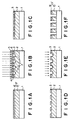
- FIG. 1A to FIG. 1F are drawings illustrating a fine pattern forming method according to a first embodiment of the present invention.
- a first resist film 2 comprising organic high molecules and a second resist film 3 comprising a photosensitive material are sequentially applied to a substrate 1 by the spin coat method or the spray method to form a two-layer resist 3'.
- a mask 4 with which a metallic fine opening pattern 6 is formed on a mask substrate 5 comprising a dielectric, such as glass is tightly contacted with the two-layer resist.
- light such as i-line (365 nm)
- near field light 7 which is effused from the opening portions of the mask 4 where no metal is formed
- a wafer having the two-layer resist 3' applied onto the substrate 1 is loaded on the mount of the exposure device, and the mask 4 is loaded over it in the vicinity thereof.
- inert gas such as N 2
- the space between the mask and the resist is evacuated to contact the mask with the resist as shown in FIG. 2B.
- the purge N 2 gas is again injected to separate the mask from the resist as shown in FIG. 2C.
- the exposed portions are made soluble in the developing solvent, resulting in a positive type pattern being formed.
- the first resist layer 2 is dry-etched with O 2 plasma, as shown in FIG. 1E, to form a fine pattern having a high aspect ratio as shown in FIG. 1F. Ion dry etching or gas etching may be performed instead of the dry etching.
- the substrate is worked by etching, vapor deposition, or the like, before the two-layer resist is peeled off.
- This peeling can be simply practiced by dissolving the first resist because the exposure, etc. have not changed the first resist in anyway.
- the peeling can also be performed by plasma ashing.
- the photosensitive resist of the second resist layer 3 may be a negative type resist, with which only the portions exposed to the projected light use insoluble in the developing solvent, and it is preferable that the thickness of the second resist layer be equal to or less than the depth to which the near field light is effused.
- the organic polymeric material for the first resist layer 2 may be any material, provided that it can be etched by oxygen plasma, and a well-known photoresist may be used. However, from the viewpoint of the resistance to plasma in dry etching the substrate, it is preferable to use an aromatic-containing polymer.
- FIG. 3A and FIG. 3B are sectional drawings for that exposure device.
- the proximity exposure technique with which the mask is brought close to the two-layer resist 3' within the reach of the near field light for exposure may be used.
- the proximity exposure By carrying out the proximity exposure, such problems as possible damage to the mask and/or wafer, and the possibility of dirt being deposited on the wafer can be eliminated, resulting in the output being improved, which allows volume production.
- FIG. 5 illustrates a method for fine pattern formation using an optical stamp according to the second embodiment of the present invention.
- a first resist layer 12 comprising organic high molecules and a second resist layer 13 comprising a photosensitive material are applied onto a substrate 11 in sequence.
- An optical stamp 14 which generates near field light from the convexity and concavity pattern by total reflection is projected onto the second resist layer 13, which is then processed for development to form a pattern.
- the first resist layer 12 is etched with the pattern in the second resist layer 13 being used as a mask to form a pattern having a high aspect ratio.
- the optical stamp is not made of a metal as with a mask, offering an advantage that it can be prepared at low cost.
- the optical stamp may be used for pattern formation by proximity exposure as stated above.
- FIG. 7 is a drawing illustrating a method for fine pattern formation using a probe according to a third embodiment of the present invention.
- a first resist layer 22 comprising organic high molecules and a second resist layer 23 comprising a photosensitive material are applied onto a substrate 21 in sequence.
- Near field light 27 is generated from the tip of a probe 24 having an opening with a diameter smaller than the wavelength for the light source, and the probe 24 is moved in the form of a desired pattern on the second resist to carry out exposure.
- the second resist layer 23 By processing the second resist layer 23 for development, a pattern is formed in the second resist layer 23.
- the first resist layer 22 is etched with the pattern in the second resist layer 23 being used as a mask to form a pattern having a high aspect ratio.
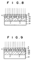
- the resist layer configuration may comprise an antireflection layer 38 between a substrate 31 and a first resist layer 32 in the configuration in which the first resist layer 32 and a second resist layer 33 are formed on the substrate 31 in this order, as shown in FIG. 8, or comprise an antireflection layer 48 between a first resist layer 42 and a second resist layer 43 which are formed on a substrate 41, as shown in FIG. 9.
- the elements in FIG. 8 and FIG. 9 which are the same as those in the above-described embodiments are each provided with the same reference numeral, and detailed description will be omitted here.
- the substrate may be a semiconductor substrate of Si, GaAs, or the like, or a substrate on the top layer of which an insulation film, such as an SiO 2 film, is formed.
- the first resist layer of the present invention is formed of a material which can be dry-etched, particularly, of an organic polymeric material. It is preferable that an intermediate mixed layer be not formed between the first resist layer and the second resist layer to be formed thereupon, and therefore, the organic polymeric material for the first resist layer is preferably a material that will not dissolve in the solvent for the second resist layer, or a material that will not dissolve at room temperature, but, through heating or other treatment, will be crosslinked in the form of a network, and thus will not practically form an intermediate mixed layer.
- An example of the latter is a resist for i-line or that for g-line which contains novolak resin and a naphtoquinone diazide compound, being used for such an application as manufacturing a semiconductor device, and which is applied to the required film thickness, and thereafter heat-treated for curing.
- a negative type resist which contains an alkaline solution soluble resin, such as novolak resin and polyhydroxy styrene, and an acidic crosslinking agent and a light acid generator, and which, after the application, is exposed to light over the entire surface for curing.
- Another example is a negative type resist which contains an alkaline solution soluble resin, such as novolak resin and polyhydroxy styrene, and a multifunctional monomer, and a photopolymerization initiator or a thermal polymerization initiator, and which, after application, is exposed to light over the entire surface or heat-treated for curing.
- an alkaline solution soluble resin such as novolak resin and polyhydroxy styrene
- a multifunctional monomer such as polyhydroxy styrene
- a photopolymerization initiator or a thermal polymerization initiator such as a photopolymerization initiator or a thermal polymerization initiator
- a composition which contains a vinyl polymer having at least one of a naphthyl group and an anthryl group in the side chain and a composition which contains a vinyl polymer having at least one of a naphthyl group and an anthryl group in the side chain, and having a group being capable of crosslinked, and a cross linking agent can be mentioned.
- an additive such as fulleren and its derivative
- a photosensitive resist material with which the near field light is projected to make only the irradiated portion or the non-irradiated portion soluble in the developing solvent, the remaining portion having a resistance to dry etching is used.
- this resist material it is preferable to use a material which contains a compound having silicon atoms, and with which the content of silicon in the solid content exceeds a certain value.
- oxygen-containing plasma the higher the content of silicon, the better, from the viewpoint of resistance to oxygen plasma.
- the content of silicon is 1% or over, and preferably, it is 4% to 50%. Particularly, it is preferable that the content of silicon be 5% to 30%.
- resist materials to be used for the second resist layer of the present invention those as disclosed in Japanese Patent Nos. 2035509, 2094657, 2597163, 2606652, 2646241, 2646288, 2646289, Japanese Unexamined Patent Publication Nos.
- materials which can be processed for development with an aqueous alkali developing solution are preferable because they produce no organic waste fluids, offer a low degree of swelling, and allow formation of a good pattern on the high developing power. More specifically, they are pattern formation materials which contain a water-insoluble and alkali-soluble silicone-containing polymer, and a photosensitive compound.
- a pattern formation material which contains a water-insoluble and alkali-soluble silicone-containing polymer, and a naphtoquinone diazide compound and/or a diazo ketone compound;
- water-insoluble and alkali-soluble silicone-containing polymer water-insoluble and alkali-soluble polysiloxane or polysilsesquioxane is more preferable.
- the solubility of which in an aqueous alkali developing solution is increased under the action of the acid and which has a functional group, polysiloxane, polysilsesquioxane, or the like having an acid-decomposable group in the side chain, as disclosed in Japanese Patent Application No. 11(1999)-24236 and Japanese Patent Application No. 11(1999)-277016, or a silicone-containing vinyl polymer having an acid-decomposable group in the side chain, as disclosed in Japanese Patent Application No. 11(1999)-298606 and Japanese Patent Application No. 11(1999)-293882, can be used.
- the positive type pattern formation material which contains a water-insoluble and alkali-soluble silicone-containing polymer, a compound generating an acid when irradiated with active light beam or radiation, and a high molecular or low molecular compound which has a group capable of being decomposed by an acid, and the solubility of which in an aqueous alkali developing solution is increased under the action of the acid, is particularly preferable.
- water-insoluble and alkali-soluble silicone-containing polymer will be described with the general chemical formulae being given below.
- the water-insoluble and alkali-soluble silicone-containing polymer those having a repetitive unit(s) expressed by the following general formula(e) [I] and/or [II], as disclosed in Japanese Patent Application No. 10(1998)-354878 and Japanese Patent Application No. 11(1999)-143614, can be mentioned.
- R denotes a hydrocarbon group which may have a hydrogen atom or a substituent.
- R' to R'''' may or may not be the same as one another, and are each a group selected from the group of chemical groups comprising the alkyl group, cycloalkyl group, alkoxy group, alkenyl group, aralkyl group, and phenyl group which may have a hydroxyl group or a substituent.
- Y is an alkyl group, alkoxy group, or siloxyl group.
- R 0 is a group selected from the group of chemical groups comprising the aliphatic hydrocarbon group and aromatic hydrocarbon group which may have a hydrogen atom, halogen atom, or a substituent.
- r, s, and t are each an integer of 1 to 3
- u, v, and w are each an integer of 1 or 2.
- l, m, n, and q are each 0 or a positive integer, and p is a positive integer.
- R ⁇ , R ⁇ , and R ⁇ each denote a single bond or -(CH 2 ) k -(Z ⁇ ) j -R ⁇ -.
- Z ⁇ denotes -OCO-, -O-, -N(R ⁇ )CO-, -COO-, or -CON(R ⁇ )-.
- R ⁇ denotes a single bond, alkylene having 1 to 12 carbon atoms, a substituted alkylene, cycloalkylene, arylene, or aralkylene.
- R ⁇ denotes a hydrogen atom, or an alkyl group having 1 to 10 carbon atoms which may have been substituted.
- k is 0 or a positive integer, and j is 0 or 1.
- water-insoluble and alkali-soluble silicone-containing polymer those having a repetitive unit(s) expressed by the following general formula(e) [III] and/or [IV], as disclosed in Japanese Patent Application No. 11(1999)-20224 and Japanese Patent Application No. 11(1999)-31591, can also be mentioned.
- R denotes a hydrocarbon group which may have a hydrogen atom or a substituent.
- R' to R'''' may or may not be the same as one another, and are each a group selected from the group of chemical groups comprising the alkyl group, cycloalkyl group, alkoxy group, alkenyl group, aralkyl group, and phenyl group which may have a hydroxyl group or a substituent.
- Y is an alkyl group, alkoxy group, or siloxyl group.
- R 0 is a group selected from the group of chemical groups comprising the aliphatic hydrocarbon group and aromatic hydrocarbon group which may have a hydrogen atom, halogen atom, or a substituent.
- l, m, n, and q are each 0 or a positive integer, and p is a positive integer.
- the compound generating an acid when irradiated with active light beam or radiation is a compound which is decomposed to generate an acid when irradiated with active light beam or radiation, as disclosed in Japanese Patent Application No. 10(1998)-354878 and Japanese Patent Application No. 11(1999)-143614, and from the known compounds generating an acid under the light which are used in the photo initiator for photo cation polymerization, the photo initiator for photo radical polymerization, the photo decolorizing agent for coloring matters, the color changing agent, the micro resist, or the like, and the mixtures of these, an appropriate one can be selected for use.
- the polymer which has a group capable of being decomposed by an acid, and the solubility of which in an aqueous alkali developing solution is increased under the action of the acid will be described.
- the polymer which has a group capable of being decomposed by an acid, and the solubility of which in an aqueous alkali developing solution is increased under the action of the acid those having a repetitive unit expressed by the following general formula [V], as disclosed in Japanese Patent Application No. 10(1998)-354878 and Japanese Patent Application No. 11(1999)-143614 or Japanese Patent Application No. 11(1999)-331568, can be mentioned.
- R 1 to R 3 , R 5 to R 7 , and R 9 to R 11 may or may not be the same as one another, and are each an alkyl group, aralkyl group, or alkoxy group which may have a hydrogen atom, a halogen atom, or a group expressed by -COZR 13 , or a substituent.
- R 4 and R 8 may or may not be the same as one another, and are each a single bond or a group having a valence of 2 to 5 which is expressed by the following formula.
- a 1 to A 5 may or may not be the same as one another, and each denote a hydrogen atom, -(R 14 ) e or a single bond, and at least one of the A 1 to A 5 denotes a single bond.
- R 14 is defined in the same manner as R 1 , to R 3 , R 5 to R 7 , and R 9 to R 11 .
- R 15 is a single bond or a group expressed by -R 30 -Y 3 -.
- Z denotes a single bond or a group expressed by -O-, -NH-, or -NR 25 -.
- R 13 and R 25 may or may not be the same as one another, and each denote an alkyl group, cycloalkyl group, or aralkyl group which may have a substituent.
- R 30 is an alkylene group or cycloalkylene group which may have a substituent.
- R 2 and R 4 or R 6 and R 8 may be bonded to each other to form the following group.
- Y 0 is synonymous to R 4 and R 8 , and Y 0 is bonded to G or Q.
- G denotes a group selected from the group of chemical groups comprising -OH, -COOH, -CONHCOR 16 , -CONHSO 2 -R 16 , and -SO 2 NH-R 16 .
- R 16 is an alkyl group, cycloalkyl group, acyl group, or aryl group which may have a substituent.
- Q denotes a group selected from the following group of chemical groups.
- R 18 , R 19 , R 21 , and R 22 may or may not be the same as one another, and is each an alkyl group having 1 to 4 carbon atoms which may have a hydrogen atom or a halogen atom as a substituent.
- R 20 is an alkyl group having 1 to 4 carbon atoms which may have a silyl group, an oxysilyl group, or a halogen atom as a substituent.
- R 23 is an alkyl group, cycloalkyl group, aralkyl group, alkenyl group, aryloxyalkyl group, aralkyloxyalkyl group, or cycloalkyl-alkyl group which may have a hydroxyl group, halogen atom, acyl group, or a substituent.
- R 17 denotes either of the following groups.
- R 26 and R 27 are each synonymous to the above R 18 , R 19 , R 21 , and R 22 .
- R 28 is an alkyl group, cycloalkyl group, aryl group, or aralkyl group which may have a substituent.
- R 26 and R 27 and/or R 28 may be bonded to one another to form a single ring or multiple ring having 4 to 9 members.
- R 29 is an alkyl group, cycloalkyl group, aryl group, aralkyl group, alkoxy group, acyl group, acylamino group, or alkoxycarbonyl group which may have a hydrogen atom, halogen atom, or a substituent.
- R 12 is an alkyl group, aralkyl group, or alkoxy group which may have a hydrogen atom, halogen atom, or a substituent, or a group expressed by -COZR 13 (Z and R 13 are synonymous to the above Z and R 13 ), or either of the following substituents.
- Z and R 15 are synonymous to the above Z and R 15 .
- R 24 is synonymous to the above R 29 .
- a, c, and d are each 0 or a positive integer, and b is a positive integer.
- e is 0 or an integer of 1 to 4; f and g are each an integer of 1 to 4; and h is an integer of 1 to 6.
- Ra, Rb, and Rc each denote a hydrocarbon group which may have a hydrogen atom, or a substituent, independently of each other. s denotes an integer of 2 or greater.
- Z denotes a single bond, -O-, -NH-, or -N(R 25 )-.
- R 13 and R 25 may or may not be the same as one another, and each denote an alkyl group, cycloalkyl group, or aralkyl group which may have a substituent.
- R 4 and R 8 may or may not be the same as one another, and each denote a group having a valence of 2 to 5 which is expressed by the following formula.
- a 1 to A 5 may or may not be the same as one another, and each denote a hydrogen atom, -R 14 or a single bond, and at least one of the A 1 to A 5 denotes a single bond.
- R 15 is a single bond or a group expressed by -R 30 -Y 3 -.
- Z denotes a single bond or a group expressed by -O-, -NH-, or -NR 25 -.
- R 14 is synonymous to R 1 to R 3 and R 5 to R 7 .
- R 30 is an alkylene group or cycloalkylene group which may have a substituent.
- R 25 is synonymous to the above R 25 .
- R 2 and R 4 or R 6 and R 8 may be bonded to each other to form the following group.
- Y 0 is defined in the same manner as R 4 and R 8 , and Y 0 is bonded to G or Q.
- G denotes a group selected from the group of chemical groups comprising -OH, -COOH, - CONHCOR 16 , -CONHSO 2 -R 16 , and -SO 2 NH-R 16 .
- R 16 is an alkyl group, cycloalkyl group, acyl group, or aryl group which may have a substituent.
- R 21 , and R 22 may or may not be the same as one another, and is each an alkyl group having 1 to 4 carbon atoms which may have a hydrogen atom or a halogen atom as a substituent.
- R 23 is an alkyl group, cycloalkyl group, aryl group, or aralkyl group which may have a substituent.
- the R 26 and R 27 may or may not be the same as one another, and are each synonymous to the R 21 and R 22 .
- R 28 is an alkyl group, cycloalkyl group, aryl group, or aralkyl group which may have a substituent.
- a is an integer of 0 or greater, and b is a positive integer.
- f and g are each an integer of 1 to 4.
- the compound which has a group capable of being crosslinked by an acid will be described.
- a compound produced by causing formaldehyde to act upon melamine, benzoguanamine, glycoluryl, or the like, or its alkyl modified substance, an epoxy compound, aldehydes, an azide compound, an organic peroxide, hexamethylenetetramine, and the like can be mentioned. partially reacted products of these and aqueous-alkali-soluble plastics can be effectively used.
- the compounds for use in the embodiments of the present invention which have an olefin unsaturated group preferably have a boiling point of 100 °C or over under the normal pressure.
Landscapes
- Physics & Mathematics (AREA)
- General Physics & Mathematics (AREA)
- Spectroscopy & Molecular Physics (AREA)
- Engineering & Computer Science (AREA)
- Architecture (AREA)
- Structural Engineering (AREA)
- Materials For Photolithography (AREA)
- Drying Of Semiconductors (AREA)
- Photosensitive Polymer And Photoresist Processing (AREA)
- Exposure Of Semiconductors, Excluding Electron Or Ion Beam Exposure (AREA)
Applications Claiming Priority (2)
| Application Number | Priority Date | Filing Date | Title |
|---|---|---|---|
| JP12338999 | 1999-04-30 | ||
| JP12338999 | 1999-04-30 |
Publications (2)
| Publication Number | Publication Date |
|---|---|
| EP1054296A2 true EP1054296A2 (de) | 2000-11-22 |
| EP1054296A3 EP1054296A3 (de) | 2002-03-06 |
Family
ID=14859373
Family Applications (1)
| Application Number | Title | Priority Date | Filing Date |
|---|---|---|---|
| EP00109254A Ceased EP1054296A3 (de) | 1999-04-30 | 2000-04-28 | Verfahren zur Herstellung feiner Strukturen |
Country Status (2)
| Country | Link |
|---|---|
| US (1) | US6497996B1 (de) |
| EP (1) | EP1054296A3 (de) |
Cited By (2)
| Publication number | Priority date | Publication date | Assignee | Title |
|---|---|---|---|---|
| US6707538B2 (en) | 2001-06-21 | 2004-03-16 | Fuji Photo Film Co., Ltd. | Near-field exposure system selectively applying linearly polarized exposure light to exposure mask |
| EP1535113A2 (de) * | 2002-09-06 | 2005-06-01 | Canon Kabushiki Kaisha | Belichtungsmethode, Belichtungsmaske und Belichtungsgerät |
Families Citing this family (12)
| Publication number | Priority date | Publication date | Assignee | Title |
|---|---|---|---|---|
| JP4017795B2 (ja) * | 1999-08-27 | 2007-12-05 | 富士フイルム株式会社 | 光波長変換素子およびその作製方法 |
| JP3772077B2 (ja) * | 2000-09-27 | 2006-05-10 | 株式会社東芝 | パターン形成方法 |
| JP2003066600A (ja) * | 2001-06-12 | 2003-03-05 | Canon Inc | フォトレジスト、これを用いた基板の加工方法、及びフォトレジストの製造方法 |
| US8403367B2 (en) * | 2001-08-02 | 2013-03-26 | Eastman Kodak Company | Authentication using near-field optical imaging |
| US6566280B1 (en) * | 2002-08-26 | 2003-05-20 | Intel Corporation | Forming polymer features on a substrate |
| TWI226501B (en) * | 2003-01-03 | 2005-01-11 | Quanta Display Inc | Method of forming a thin film transistor liquid crystal display |
| JP4194514B2 (ja) * | 2003-06-26 | 2008-12-10 | キヤノン株式会社 | 露光用マスクの設計方法及び製造方法 |
| JP2005085922A (ja) * | 2003-09-08 | 2005-03-31 | Canon Inc | マスク作製方法及び微小開口を有するマスク |
| JP4574250B2 (ja) * | 2004-06-30 | 2010-11-04 | キヤノン株式会社 | フォトマスク |
| JP4247198B2 (ja) * | 2005-03-31 | 2009-04-02 | 株式会社東芝 | 半導体装置の製造方法 |
| US7297636B1 (en) * | 2007-01-31 | 2007-11-20 | Advanced Micro Devices, Inc. | Methods for fabricating device features having small dimensions |
| WO2014159427A1 (en) * | 2013-03-14 | 2014-10-02 | Applied Materials, Inc | Resist hardening and development processes for semiconductor device manufacturing |
Family Cites Families (11)
| Publication number | Priority date | Publication date | Assignee | Title |
|---|---|---|---|---|
| US4782008A (en) * | 1985-03-19 | 1988-11-01 | International Business Machines Corporation | Plasma-resistant polymeric material, preparation thereof, and use thereof |
| US4822716A (en) * | 1985-12-27 | 1989-04-18 | Kabushiki Kaisha Toshiba | Polysilanes, Polysiloxanes and silicone resist materials containing these compounds |
| JP2619358B2 (ja) * | 1986-01-08 | 1997-06-11 | 株式会社日立製作所 | 感光性樹脂組成物 |
| US4737425A (en) * | 1986-06-10 | 1988-04-12 | International Business Machines Corporation | Patterned resist and process |
| US4931351A (en) * | 1987-01-12 | 1990-06-05 | Eastman Kodak Company | Bilayer lithographic process |
| DE3806088A1 (de) * | 1988-02-26 | 1989-09-07 | Basf Ag | Photoreaktive polymere und verfahren zur herstellung eines zweilagenresists |
| JP3001607B2 (ja) * | 1989-04-24 | 2000-01-24 | シーメンス、アクチエンゲゼルシヤフト | 二層法における寸法安定な構造転写方法 |
| JP2793251B2 (ja) * | 1989-05-09 | 1998-09-03 | 株式会社東芝 | パターン形成方法 |
| EP0534273B1 (de) * | 1991-09-27 | 1996-05-15 | Siemens Aktiengesellschaft | Verfahren zur Erzeugung eines Bottom-Resists |
| US5532105A (en) * | 1992-08-07 | 1996-07-02 | Hitachi Chemical Company, Ltd. | Photolithographically viahole-forming photosensitive element comprising two photosensitive layers for the fabrication process of multilayer wiring board |
| JPH11317345A (ja) | 1998-04-30 | 1999-11-16 | Ebara Corp | 微細パターンの転写加工方法 |
-
2000
- 2000-04-28 EP EP00109254A patent/EP1054296A3/de not_active Ceased
- 2000-05-01 US US09/562,076 patent/US6497996B1/en not_active Expired - Fee Related
Non-Patent Citations (7)
| Title |
|---|
| BRITTAIN S. ET AL: "SOFT LITHOGRAPHY AND MICROFABRICATION", PHYSICS WORLD, vol. 11, no. 5, 1 May 1998 (1998-05-01), BRISTOL, GB, pages 31 - 36, XP008022000 * |
| JOURNAL ARTICLE: "Lithographie mit "Lichtstempeln", TECHNISCHE RUNDSCHAU TRANSFER, vol. 9055, no. 19, 9 October 1998 (1998-10-09), EDITION COLIBRI AG., WABERN, CH, pages 20, XP000824413 * |
| JOURNAL ARTICLE: "UTILIZING OPTICAL LITHOGRAPHY IN THE SUB-MICRON DIMENSIONAL REGIME", IBM TECHNICAL DISCLOSURE BULLETIN, vol. 33, no. 5, 1 October 1990 (1990-10-01), IBM CORP. NEW YORK, US, pages 187/188, XP000107428 * |
| KRAUSCH G.; MLYNEK J.: "Surface modification in the optical near field", MICROELECTRONIC ENGINEERING, vol. 32, no. 1, 1 September 1996 (1996-09-01), ELSEVIER PUBLISHERS BV., AMSTERDAM, NL, pages 219 - 228, XP004013435 * |
| ONO T. ET AL: "SUBWAVELENGTH PATTERN TRANSFER BY NEAR-FIELD PHOTOLITHOGRAPHY", JAPANESE JOURNAL OF APPLIED PHYSICS, vol. 37, no. 12B, 1 December 1998 (1998-12-01), JAPAN SOCIETY OF APPLIED PHYSICS, TOKYO, JP, pages 6745 - 6749, XP000880249 * |
| ROGERS J. ET AL: "USING AN ELASTOMERIC PHASE MASK FOR SUB-100 NM PHOTOLITHOGRAPHY IN THE OPTICAL NEAR FIELD", APPLIED PHYSICS LETTERS, vol. 70, no. 20, 19 May 1997 (1997-05-19), pages 2658 - 2660 * |
| SCHMID H. ET AL: "Light-coupling masks for lensless, sub-wavelenth optical lithography", APPLIED PHYSICS LETTERS, vol. 72, no. 19, 11 May 1998 (1998-05-11), pages 2379 - 2381 * |
Cited By (2)
| Publication number | Priority date | Publication date | Assignee | Title |
|---|---|---|---|---|
| US6707538B2 (en) | 2001-06-21 | 2004-03-16 | Fuji Photo Film Co., Ltd. | Near-field exposure system selectively applying linearly polarized exposure light to exposure mask |
| EP1535113A2 (de) * | 2002-09-06 | 2005-06-01 | Canon Kabushiki Kaisha | Belichtungsmethode, Belichtungsmaske und Belichtungsgerät |
Also Published As
| Publication number | Publication date |
|---|---|
| US6497996B1 (en) | 2002-12-24 |
| EP1054296A3 (de) | 2002-03-06 |
Similar Documents
| Publication | Publication Date | Title |
|---|---|---|
| US5017461A (en) | Formation of a negative resist pattern utilize water-soluble polymeric material and photoacid generator | |
| US6277750B1 (en) | Composition for bottom reflection preventive film and novel polymeric dye for use in the same | |
| JP3408415B2 (ja) | 光酸発生剤をしてなる反射防止コーティング組成物 | |
| JP4467857B2 (ja) | 電子線露光による193nm感光性フォトレジスト材料の改変 | |
| US6900001B2 (en) | Method for modifying resist images by electron beam exposure | |
| US6497996B1 (en) | Fine pattern forming method | |
| JP2501292B2 (ja) | 酸感応ポリマおよびホトレジスト構造の作成方法 | |
| US20030108818A1 (en) | Method and apparatus for modification of chemically amplified photoresist by electron beam exposure | |
| US6319654B1 (en) | Process for forming a photoresist pattern by top surface imaging process | |
| JP4105106B2 (ja) | 微細パターン形成方法 | |
| US8034546B2 (en) | Use of methanofullerne derivatives as resist materials and method for forming a resist layer | |
| US6168897B1 (en) | Method of forming patterns | |
| JP3239329B2 (ja) | マイクロリソグラフィ構造 | |
| US4912018A (en) | High resolution photoresist based on imide containing polymers | |
| WO1990003598A1 (en) | Multifunctional photolithographic compositions | |
| JP2001021710A (ja) | 回折格子作製方法 | |
| JP2007017976A (ja) | 多層リソグラフィプロセスにおいて用いられる複素環芳香族構造物を含む基層組成物、リソグラフィ構造物、材料層または材料要素を基板上に形成させる方法 | |
| JPH09235326A (ja) | アセタール基を含有するアルコキシ−スチレン重合体とその製造方法及びアルコキシ−スチレン重合体を主要成分とする化学増幅型フォトレジスト材料 | |
| US6821718B2 (en) | Radiation sensitive silicon-containing negative resists and use thereof | |
| US20030235784A1 (en) | Organic anti-reflective coating composition and method for forming photoresist patterns using the same | |
| JP2001015427A (ja) | 微細パターン形成方法 | |
| US6669995B1 (en) | Method of treating an anti-reflective coating on a substrate | |
| JP2001015426A (ja) | 微細パターン形成方法 | |
| US6989227B2 (en) | E-beam curable resist and process for e-beam curing the resist | |
| TWI273349B (en) | A low outgassing and non-crosslinking series of polymers for EUV negative tone photoresists |
Legal Events
| Date | Code | Title | Description |
|---|---|---|---|
| PUAI | Public reference made under article 153(3) epc to a published international application that has entered the european phase |
Free format text: ORIGINAL CODE: 0009012 |
|
| AK | Designated contracting states |
Kind code of ref document: A2 Designated state(s): CH DE FR GB LI NL Kind code of ref document: A2 Designated state(s): AT BE CH CY DE DK ES FI FR GB GR IE IT LI LU MC NL PT SE |
|
| AX | Request for extension of the european patent |
Free format text: AL;LT;LV;MK;RO;SI |
|
| PUAL | Search report despatched |
Free format text: ORIGINAL CODE: 0009013 |
|
| AK | Designated contracting states |
Kind code of ref document: A3 Designated state(s): AT BE CH CY DE DK ES FI FR GB GR IE IT LI LU MC NL PT SE |
|
| AX | Request for extension of the european patent |
Free format text: AL;LT;LV;MK;RO;SI |
|
| RIC1 | Information provided on ipc code assigned before grant |
Free format text: 7G 03F 7/09 A, 7G 03F 7/095 B, 7G 03F 7/075 B |
|
| 17P | Request for examination filed |
Effective date: 20020417 |
|
| AKX | Designation fees paid |
Free format text: CH DE FR GB LI NL |
|
| RBV | Designated contracting states (corrected) |
Designated state(s): DE FR GB NL |
|
| RAP1 | Party data changed (applicant data changed or rights of an application transferred) |
Owner name: FUJIFILM CORPORATION |
|
| 17Q | First examination report despatched |
Effective date: 20070410 |
|
| STAA | Information on the status of an ep patent application or granted ep patent |
Free format text: STATUS: THE APPLICATION HAS BEEN REFUSED |
|
| 18R | Application refused |
Effective date: 20090507 |