EP1056102A2 - Nichtreduzierende dielektrische keramische Zusammensetzung und monolithischer keramischer Kondensator - Google Patents
Nichtreduzierende dielektrische keramische Zusammensetzung und monolithischer keramischer Kondensator Download PDFInfo
- Publication number
- EP1056102A2 EP1056102A2 EP00106628A EP00106628A EP1056102A2 EP 1056102 A2 EP1056102 A2 EP 1056102A2 EP 00106628 A EP00106628 A EP 00106628A EP 00106628 A EP00106628 A EP 00106628A EP 1056102 A2 EP1056102 A2 EP 1056102A2
- Authority
- EP
- European Patent Office
- Prior art keywords
- dielectric ceramic
- ceramic
- nonreducing
- monolithic
- internal electrodes
- Prior art date
- Legal status (The legal status is an assumption and is not a legal conclusion. Google has not performed a legal analysis and makes no representation as to the accuracy of the status listed.)
- Granted
Links
Images
Classifications
-
- H—ELECTRICITY
- H01—ELECTRIC ELEMENTS
- H01G—CAPACITORS; CAPACITORS, RECTIFIERS, DETECTORS, SWITCHING DEVICES, LIGHT-SENSITIVE OR TEMPERATURE-SENSITIVE DEVICES OF THE ELECTROLYTIC TYPE
- H01G4/00—Fixed capacitors; Processes of their manufacture
- H01G4/002—Details
- H01G4/018—Dielectrics
- H01G4/06—Solid dielectrics
- H01G4/08—Inorganic dielectrics
- H01G4/12—Ceramic dielectrics
- H01G4/1209—Ceramic dielectrics characterised by the ceramic dielectric material
- H01G4/1218—Ceramic dielectrics characterised by the ceramic dielectric material based on titanium oxides or titanates
- H01G4/1227—Ceramic dielectrics characterised by the ceramic dielectric material based on titanium oxides or titanates based on alkaline earth titanates
-
- H—ELECTRICITY
- H01—ELECTRIC ELEMENTS
- H01G—CAPACITORS; CAPACITORS, RECTIFIERS, DETECTORS, SWITCHING DEVICES, LIGHT-SENSITIVE OR TEMPERATURE-SENSITIVE DEVICES OF THE ELECTROLYTIC TYPE
- H01G4/00—Fixed capacitors; Processes of their manufacture
- H01G4/002—Details
- H01G4/018—Dielectrics
- H01G4/06—Solid dielectrics
- H01G4/08—Inorganic dielectrics
- H01G4/12—Ceramic dielectrics
-
- C—CHEMISTRY; METALLURGY
- C04—CEMENTS; CONCRETE; ARTIFICIAL STONE; CERAMICS; REFRACTORIES
- C04B—LIME, MAGNESIA; SLAG; CEMENTS; COMPOSITIONS THEREOF, e.g. MORTARS, CONCRETE OR LIKE BUILDING MATERIALS; ARTIFICIAL STONE; CERAMICS; REFRACTORIES; TREATMENT OF NATURAL STONE
- C04B35/00—Shaped ceramic products characterised by their composition; Ceramics compositions; Processing powders of inorganic compounds preparatory to the manufacturing of ceramic products
- C04B35/01—Shaped ceramic products characterised by their composition; Ceramics compositions; Processing powders of inorganic compounds preparatory to the manufacturing of ceramic products based on oxide ceramics
- C04B35/46—Shaped ceramic products characterised by their composition; Ceramics compositions; Processing powders of inorganic compounds preparatory to the manufacturing of ceramic products based on oxide ceramics based on titanium oxides or titanates
- C04B35/462—Shaped ceramic products characterised by their composition; Ceramics compositions; Processing powders of inorganic compounds preparatory to the manufacturing of ceramic products based on oxide ceramics based on titanium oxides or titanates based on titanates
- C04B35/465—Shaped ceramic products characterised by their composition; Ceramics compositions; Processing powders of inorganic compounds preparatory to the manufacturing of ceramic products based on oxide ceramics based on titanium oxides or titanates based on titanates based on alkaline earth metal titanates
- C04B35/468—Shaped ceramic products characterised by their composition; Ceramics compositions; Processing powders of inorganic compounds preparatory to the manufacturing of ceramic products based on oxide ceramics based on titanium oxides or titanates based on titanates based on alkaline earth metal titanates based on barium titanates
- C04B35/4682—Shaped ceramic products characterised by their composition; Ceramics compositions; Processing powders of inorganic compounds preparatory to the manufacturing of ceramic products based on oxide ceramics based on titanium oxides or titanates based on titanates based on alkaline earth metal titanates based on barium titanates based on BaTiO3 perovskite phase
Definitions
- the present invention relates to nonreducing dielectric ceramics and monolithic ceramic capacitors provided with dielectric ceramic layers composed of the nonreducing dielectric ceramics. More particularly, the invention relates to monolithic ceramic capacitors which are advantageously used under the conditions of high-frequency AC or high to medium voltage DC and are provided with internal electrodes composed of base metals, and to nonreducing dielectric ceramics for constituting dielectric ceramic layers of the monolithic ceramic capacitors.
- a conventional monolithic capacitor is usually produced in a method described below.
- a plurality of ceramic green sheets containing a dielectric material for forming dielectric ceramic layers are prepared, in which the surface of each ceramic green sheet is coated with an electrode material for forming internal electrodes.
- the dielectric material for example, a material containing BaTiO 3 as a principal constituent is used.
- the plurality of ceramic green sheets each coated with the electrode material are laminated and are subjected to thermal compression, and the resultant compact is fired, and thus a ceramic laminate provided with internal electrodes is obtained.
- a monolithic ceramic capacitor is obtained.
- a material which is not oxidized by the firing of ceramic laminates has been selected.
- Exampies of such a material includes noble metals such as platinum, gold, palladium, and silver-palladium alloys.
- noble metals such as platinum, gold, palladium, and silver-palladium alloys.
- materials for internal electrodes have excellent characteristics, they are very expensive, resulting in an increase in production cost of monolithic ceramic capacitors.
- the base metals are easily oxidized in high-temperature, oxidizing atmospheres, which wins the function as the internal electrodes.
- firing In order to use base metals as materials for internal electrodes of monolithic ceramic capacitors, firing must be performed in a neutral or reducing atmosphere to obtain ceramic laminates.
- Japanese Examined Patent Publication No. 61-14611 discloses a BaTiO 3 -(Mg, Zn, Sr, Ca)O-B 2 O 3 -SiO 2 -based dielectric ceramic
- Japanese Unexamined Patent Publication No. 7-272971 discloses a (Ba, M, L)(Ti, R)O 3 -based dielectric ceramic (where M is Mg or Zn, L is Ca or Sr, and R is Sc, Y, or a rare-earth element).
- monolithic ceramic capacitors are increasingly used under high-voltage DC conditions.
- the conventional monolithic ceramic capacitors which particularly uses nickel as the material for internal electrodes are intended to be used at relatively low electric field intensity, if they are used at high electric field intensity, insulating properties, dielectric strength, and reliability are greatly deteriorated, which is disadvantageous.
- a nonreducing dielectric ceramic in accordance with the present invention has a perovskite structure represented by the formula ABO 3 with a principal crystal phase containing barium titanate as a principal constituent.
- the crystal axis ratio c/a determined by an X-ray diffraction method at a temperature of -25°C or more satisfies the relationship 1.000 ⁇ c/a ⁇ 1.003. That is, the crystal structure includes a cubic system or a crystal system analogous to a cubic system.
- the phase transition point of the principal crystal phase namely, the temperature at which the variation in the relative dielectric constant reaches the sharp maximum value (peak)
- a barium titanate-based dielectric ceramic has the cubic system at a temperature that is equal to or greater than the phase transition point, i.e., the Curie point and has the tetragonal system at a temperature below the phase transition point.
- the nonreducing dielectric ceramic contains at least one rare-earth element selected from the group consisting of La, Ce, Pr, Nd, Sm, Eu, Gd, Tb, Dy, Ho, Er, Tm, Yb, Lu, Y, and Sc. If such a rare-earth element is contained, the dielectric ceramic used under DC conditions can have satisfactory life properties.
- a monolithic ceramic capacitor in accordance with the present invention includes a plurality of dielectric ceramic layers, internal electrodes formed between the dielectric ceramic layers, and external electrodes electrically connected to the internal electrodes.
- the dielectric ceramic layers are composed of the nonreducing dielectric ceramic in accordance with the present invention described above.
- the internal electrodes of the monolithic ceramic capacitor are composed of nickel, a nickel alloy, copper, or a copper alloy.
- each external electrode of the monolithic ceramic capacitor includes a first layer composed of a sintered layer containing a powdered conductive metal or a powdered conductive metal with glass frit added thereto, and a second layer composed of a plating layer.
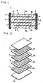
- FIG. 1 is a sectional view showing a monolithic ceramic capacitor 1 of an embodiment of the present invention and FIG. 2 is an assembly view of a ceramic laminate 3 provided in the monolithic ceramic capacitor 1 shown in FIG. 1.
- the monolithic ceramic capacitor 1 includes a ceramic laminate 3, which is a rectangular parallelepiped, obtained by laminating a plurality of dielectric ceramic layers 2a and 2b with internal electrodes 4 therebetween.
- An external electrode 5 is formed on each side of the ceramic laminate 3 so as to be electrically connected to specific internal electrodes 4.
- a first plating layer 6 composed of nickel, copper, or the like is formed on the external electrode 5, and a second plating layer 7 composed of solder, tin, or the like is further formed thereon.
- a method of fabricating the monolithic ceramic capacitor 1 will be described in sequence.
- a barium titanate-based starting powder as a principal constituent of dielectric ceramic layers 2a and 2b is prepared, which is weighed and mixed so as to satisfy the predetermined composition.
- a nonreducing dielectric ceramic having a perovskite structure represented by the formula ABO 3 with a principal crystal phase containing barium titanate as a principal constituent is produced.
- the crystal axis ratio c/a determined by an X-ray diffraction method at a temperature of -25°C or more satisfies the relationship 1.000 ⁇ c/a ⁇ 1.003.
- the phase transition point of the principal crystal phase is less than -25°C.
- the staring powder contains, as required, at least one rare-earth element selected from the group consisting of La, Ce, Pr, Nd, Sm, Eu, Gd, Tb, Dy, Ho, Er, Tm, Yb, Lu, Y, and Sc, for example, in the form of an oxide thereof.
- An internal electrode 4 containing a base metal, such as nickel, a nickel alloy, copper, or a copper alloy, as a conductive component is formed on one of the principal surfaces of each of the ceramic green sheets for the dielectric ceramic layers 2b.
- the internal electrodes 4 may be formed by printing such as screen-printing, vapor deposition, plating, or the like.
- the ceramic laminate 3 is obtained.
- the external electrodes 5 are formed on both sides of the ceramic laminate 3 so as to be electrically connected to specific internal electrodes 4.
- the same material as that for the internal electrodes 4 may be used.
- silver, palladium, a silver-palladium alloy, copper, a copper alloy, etc. may be used, or metal powders thereof added with glass frit, such as B 2 O 3 -SiO 2 -BaO-based glass or Li 2 O-SiO 2 -BaO-based glass may be used.
- An appropriate material is selected depending on the application of the monolithic ceramic capacitor 1, the place where the monolithic ceramic capacitor 1 is used, etc.
- the external electrodes 5 are typically formed by applying a metallic powder paste to the ceramic laminate 3 which has been obtained by firing, followed by baking, the metallic powder paste may be applied to the green ceramic laminate before firing and the external electrodes 5 may be formed by firing simultaneously with the ceramic laminate 3.
- the first plating layer 6 is then formed by plating nickel, copper, or the like on the external electrodes 5.
- the second plating layer 7 composed of solder, tin, or the like is formed on the first plating layer 6, and thus the monolithic ceramic capacitor 1 is completed. It may be possible to omit forming conductive layers, such as plating layers described above, on the external electrodes 5, depending on the application of the monolithic ceramic capacitor.
- the loss and heat emission during use at high frequencies and high voltages or high currents can be reduced, the insulation resistance in the AC high-temperature load or DC high-temperature load can be stabilized, and a base metal such as nickel or a nickel alloy can be used as the material for the internal electrodes 4 without any problems.
- nonreducing dielectric ceramic and the monolithic ceramic capacitor in accordance with the present invention will be described in more detail based on an example.
- powders of BaCO 3 , CaCO 3 , SrCO 3 , TiO 2 , ZrO 2 , BaTiO 3 , CaZrO 3 , SrTiO 3 , La 2 O 3 , CeO 2 , Pr 6 O 11 , Nd 2 O 3 , Sm 2 O 3 , Ho 2 O 3 , Dy 2 O 3 , Gd 2 O 3 , Eu 2 O 3 , Tb 2 O 3 , Er 2 O 3 , Tm 2 O 3 , Yb 2 O 3 , Lu 2 O 3 , Y 2 O 3 , Sc 2 O 3 , MgO, MnCO 3 , and SiO 2 having purities of 99% or more were prepared.
- a polyvinyl butyral-based binder and an organic solvent such as ethanol were added to the weighed powders of the individual samples, wet blending was performed with a ball mill, and ceramic slurries were obtained.
- the ceramic slurries were formed into sheets by a doctor blade process, and rectangular ceramic green sheets having a thickness of 25 ⁇ m were obtained.
- a conductive paste containing nickel as a principal constituent was printed on specific ceramic green sheets, and conductive paste layers for constituting internal electrodes were formed.
- a plurality of ceramic green sheets provided with the conductive paste layers were laminated in such a manner that the ends in which the conductive paste layers were exposed alternately faced different ends of the laminate to be formed, and a ceramic green sheet not provided with conductive paste layers was disposed on each of the upper and lower surfaces of the laminate. Press-bonding was then performed, and thus a green ceramic laminate was obtained.
- the green ceramic laminate was heated at 350°C in a nitrogen atmosphere, and after the binder was removed, firing was performed for 2 hours at a temperature in the range of 1,200°C to 1,350°C in a reducing atmosphere comprising gases of H 2 , N 2 , and H 2 O having an oxygen partial pressure of 10 -9 to 10 -12 MPa, and a sintered ceramic laminate was obtained.
- a conductive paste containing B 2 O 3 -Li 2 O-SiO 2 -BaO-based glass frit and silver powder was applied to both ends of the sintered ceramic laminate, and baking was performed at 600°C in a nitrogen atmosphere, and thus external electrodes which are electrically connected to the internal electrodes were formed.
- a nickel plating solution composed of nickel sulfate, nickel chloride, and boric acid was prepared, and nickel plating was performed on the external electrodes by barrel plating.
- a solder plating solution composed of an alkanol-sulfonic acid bath (AS bath) was prepared, and solder plating was performed on the nickel plating layer by barrel plating, and thus a monolithic ceramic capacitor was obtained.
- the resultant monolithic ceramic capacitor had outer dimensions in which the width was 3.2 mm, the length was 4.5 mm, and the thickness was 1.0 mm, and the dielectric ceramic layers interposed between the internal electrodes had a thickness of 20 ⁇ m.
- the effective counter area of each internal electrode was 8.8 ⁇ 10 -6 m 2 . With respect to the total number of the effective dielectric ceramic layers, firing was performed so that the capacitance was 50 nF.
- the crystal axis ratio c/a was determined by a process in which the dielectric ceramic constituting the dielectric ceramic layers was subjected to X-ray diffraction analysis at temperatures of -25°C and +25°C, respectively, the results thereof were analyzed by Rietveld method, and X-ray profile fitting was performed, and then lattice constants were computed.
- the capacitance of the monolithic capacitor was measured using an automatic bridge-type meter, and the variation in the capacitance in relation to the temperature change was obtained.
- the temperature at which the variation in the capacitance reached the sharp maximum value was defined as the phase transition point.
- the variation in the capacitance in relation to the temperature change was measured based on the capacitance at 25°C, at a frequency of 1 kHz, and at 0.02 V rms.
- the capacitance of the monolithic ceramic capacitor was measured using an automatic bridge-type meter at a frequency of 1 kHz, at 1 V rms, and at 25°C.
- the relative dielectric constant was computed based on the capacitance measured.
- the rise of the temperature was evaluated.
- the monolithic ceramic capacitor which was placed in a thermostatic bath maintained at 25°C, was electrically connected to an AC power supply, and a high-frequency high voltage of 100 kHz, 100 Vp-p was applied to the monolithic capacitor continuously for 5 minutes.
- a difference between the temperature of the monolithic ceramic capacitor and the ambient temperature was measured using an infrared radiation thermometer.
- the rate of samples which were defective in insulation resistance was evaluated.
- a high-frequency high voltage of 100 kHz, 100 Vp-p was applied to the monolithic ceramic capacitor in a thermostatic bath at 100°C, and after 250 hours, the monolithic ceramic capacitor was retrieved from the thermostatic bath, and then the insulation resistance was measured at 25°C at 500 V DC.
- the monolithic capacitor which exhibited a resistance of 10 6 ⁇ or less was defined as being defective.
- phase transition point was higher than -25°C.
- the c/a ratio at -25°C exceeded 1.003, which was relatively large. Consequently, with respect to the heat emission when a high-frequency high voltage was applied, the temperature rise exceeded 20°C or thermal runaway occurred, resulting in breakdown.
- the nonreducing dielectric ceramic contains such a rare-earth element.
- rare-earth elements as oxides are incorporated in starting powders, rare-earth elements may be incorporated as alkoxides, metallic organic compounds, or the like.
- phase transition point of the principal crystal phase is discussed, even if a secondary phase exists, characteristics are not substantially affected.
- SiO 2 is used as a sintering additive, even if glass is used as a sintering additive for the purpose of low-temperature sintering, characteristics are not substantially affected.
- a monolithic ceramic capacitor is obtained in which loss and heat emission are decreased when used at high frequencies and high voltages or high currents, and stable insulation resistance is exhibited in the AC high-temperature load or DC high-temperature load.
- a base metal such as nickel, a nickel alloy, copper, or a copper alloy can be used as the material for internal electrodes without any problems.
- the monolithic ceramic capacitor used under DC conditions can have satisfactory life properties.
Landscapes
- Engineering & Computer Science (AREA)
- Chemical & Material Sciences (AREA)
- Ceramic Engineering (AREA)
- Power Engineering (AREA)
- Manufacturing & Machinery (AREA)
- Materials Engineering (AREA)
- Microelectronics & Electronic Packaging (AREA)
- Inorganic Chemistry (AREA)
- Structural Engineering (AREA)
- Organic Chemistry (AREA)
- Ceramic Capacitors (AREA)
- Compositions Of Oxide Ceramics (AREA)
- Fixed Capacitors And Capacitor Manufacturing Machines (AREA)
- Inorganic Insulating Materials (AREA)
Applications Claiming Priority (2)
| Application Number | Priority Date | Filing Date | Title |
|---|---|---|---|
| JP14274299 | 1999-05-24 | ||
| JP11142742A JP2000327414A (ja) | 1999-05-24 | 1999-05-24 | 耐還元性誘電体セラミックおよび積層セラミックコンデンサ |
Publications (3)
| Publication Number | Publication Date |
|---|---|
| EP1056102A2 true EP1056102A2 (de) | 2000-11-29 |
| EP1056102A3 EP1056102A3 (de) | 2006-05-24 |
| EP1056102B1 EP1056102B1 (de) | 2009-07-22 |
Family
ID=15322530
Family Applications (1)
| Application Number | Title | Priority Date | Filing Date |
|---|---|---|---|
| EP00106628A Expired - Lifetime EP1056102B1 (de) | 1999-05-24 | 2000-03-28 | Nichtreduzierende dielektrische keramische Zusammensetzung und monolithischer keramischer Kondensator |
Country Status (6)
| Country | Link |
|---|---|
| US (1) | US6259594B1 (de) |
| EP (1) | EP1056102B1 (de) |
| JP (1) | JP2000327414A (de) |
| KR (1) | KR100400154B1 (de) |
| CN (1) | CN1216382C (de) |
| DE (1) | DE60042577D1 (de) |
Cited By (2)
| Publication number | Priority date | Publication date | Assignee | Title |
|---|---|---|---|---|
| WO2003069642A1 (en) * | 2002-02-13 | 2003-08-21 | Matsushita Electric Industrial Co., Ltd. | Ceramic capacitor and method of manufacturing the same |
| EP1178024A3 (de) * | 2000-07-31 | 2004-03-03 | Murata Manufacturing Co., Ltd. | Dielektrischer keramischer Körper, resistent gegen Reduktion, und keramischer Vielschichtkondensator |
Families Citing this family (16)
| Publication number | Priority date | Publication date | Assignee | Title |
|---|---|---|---|---|
| JP3391268B2 (ja) * | 1998-01-20 | 2003-03-31 | 株式会社村田製作所 | 誘電体セラミックおよびその製造方法、ならびに、積層セラミック電子部品およびその製造方法 |
| JP3417911B2 (ja) | 2000-08-21 | 2003-06-16 | ティーディーケイ株式会社 | 誘電体磁器組成物の製造方法と誘電体層含有電子部品の製造方法 |
| JP3341003B2 (ja) | 2000-12-25 | 2002-11-05 | ティーディーケイ株式会社 | 誘電体磁器組成物および電子部品 |
| JP2002234769A (ja) * | 2001-02-01 | 2002-08-23 | Murata Mfg Co Ltd | チタン酸バリウム粉末の製造方法、チタン酸バリウム粉末、誘電体セラミックおよび積層セラミックコンデンサ |
| JP2003002739A (ja) * | 2001-06-19 | 2003-01-08 | Murata Mfg Co Ltd | チタン酸バリウム粉末の製造方法、チタン酸バリウム粉末およびその評価方法、誘電体セラミック、ならびに積層セラミックコンデンサ |
| JP4506090B2 (ja) * | 2003-03-25 | 2010-07-21 | 株式会社村田製作所 | 誘電体セラミックおよび積層セラミックコンデンサ |
| JP4782552B2 (ja) * | 2005-11-28 | 2011-09-28 | 京セラ株式会社 | 誘電体磁器 |
| JP4941702B2 (ja) * | 2006-03-10 | 2012-05-30 | Tdk株式会社 | セラミック粉末及びこれを用いた導電ペースト、積層セラミック電子部品、その製造方法 |
| JP5132972B2 (ja) * | 2007-04-09 | 2013-01-30 | 太陽誘電株式会社 | 誘電体セラミックス及びその製造方法並びに積層セラミックコンデンサ |
| JP5142649B2 (ja) * | 2007-09-27 | 2013-02-13 | 京セラ株式会社 | 誘電体磁器およびコンデンサ |
| JP5142651B2 (ja) * | 2007-09-27 | 2013-02-13 | 京セラ株式会社 | 誘電体磁器およびコンデンサ |
| JP5142666B2 (ja) * | 2007-10-26 | 2013-02-13 | 京セラ株式会社 | 誘電体磁器およびコンデンサ |
| JP5142665B2 (ja) * | 2007-10-26 | 2013-02-13 | 京セラ株式会社 | 誘電体磁器およびコンデンサ |
| JP5094572B2 (ja) * | 2008-03-26 | 2012-12-12 | 京セラ株式会社 | 積層セラミックコンデンサ |
| KR102037264B1 (ko) * | 2014-12-15 | 2019-10-29 | 삼성전기주식회사 | 기판 내장용 소자, 그 제조 방법 및 소자 내장 인쇄회로기판 |
| CN116918014A (zh) * | 2021-03-31 | 2023-10-20 | 株式会社村田制作所 | 层叠陶瓷电容器 |
Family Cites Families (8)
| Publication number | Priority date | Publication date | Assignee | Title |
|---|---|---|---|---|
| JP2753887B2 (ja) * | 1989-09-29 | 1998-05-20 | 京セラ株式会社 | コンデンサー内蔵複合回路基板 |
| US5202814A (en) * | 1990-03-13 | 1993-04-13 | Murata Manufacturing Co., Ltd. | Nonreducing dielectric ceramic composition |
| US5600533A (en) * | 1994-06-23 | 1997-02-04 | Murata Manufacturing Co., Ltd. | Multilayer ceramic capacitor having an anti-reducing agent |
| CN1092391C (zh) * | 1994-10-19 | 2002-10-09 | Tdk株式会社 | 多层瓷介片状电容器 |
| JP3024536B2 (ja) * | 1995-12-20 | 2000-03-21 | 株式会社村田製作所 | 積層セラミックコンデンサ |
| JP3180690B2 (ja) * | 1996-07-19 | 2001-06-25 | 株式会社村田製作所 | 積層セラミックコンデンサ |
| EP0988637B1 (de) * | 1997-10-08 | 2005-12-21 | Ferro (Holland) B.V. | Keramischer vielschichtkondensator |
| DE19902153B4 (de) * | 1998-01-20 | 2005-03-10 | Murata Manufacturing Co | Verfahren und Bariumtitanat-Pulver zur Herstellung von dielektrischer Keramik |
-
1999
- 1999-05-24 JP JP11142742A patent/JP2000327414A/ja active Pending
-
2000
- 2000-03-28 EP EP00106628A patent/EP1056102B1/de not_active Expired - Lifetime
- 2000-03-28 DE DE60042577T patent/DE60042577D1/de not_active Expired - Lifetime
- 2000-05-24 US US09/577,957 patent/US6259594B1/en not_active Expired - Lifetime
- 2000-05-24 KR KR10-2000-0028043A patent/KR100400154B1/ko not_active Expired - Lifetime
- 2000-05-24 CN CN001176749A patent/CN1216382C/zh not_active Expired - Lifetime
Cited By (3)
| Publication number | Priority date | Publication date | Assignee | Title |
|---|---|---|---|---|
| EP1178024A3 (de) * | 2000-07-31 | 2004-03-03 | Murata Manufacturing Co., Ltd. | Dielektrischer keramischer Körper, resistent gegen Reduktion, und keramischer Vielschichtkondensator |
| WO2003069642A1 (en) * | 2002-02-13 | 2003-08-21 | Matsushita Electric Industrial Co., Ltd. | Ceramic capacitor and method of manufacturing the same |
| US6845002B2 (en) | 2002-02-13 | 2005-01-18 | Matsushita Electric Industrial Co., Ltd. | Ceramic capacitor and method of manufacturing the same |
Also Published As
| Publication number | Publication date |
|---|---|
| CN1216382C (zh) | 2005-08-24 |
| KR20010020897A (ko) | 2001-03-15 |
| US6259594B1 (en) | 2001-07-10 |
| KR100400154B1 (ko) | 2003-10-01 |
| EP1056102B1 (de) | 2009-07-22 |
| JP2000327414A (ja) | 2000-11-28 |
| EP1056102A3 (de) | 2006-05-24 |
| DE60042577D1 (de) | 2009-09-03 |
| CN1274931A (zh) | 2000-11-29 |
Similar Documents
| Publication | Publication Date | Title |
|---|---|---|
| KR100438517B1 (ko) | 내환원성 유전체 세라믹 콤팩트 및 적층 세라믹 커패시터 | |
| KR100326951B1 (ko) | 유전체 세라믹 조성물 및 모놀리식 세라믹 커패시터 | |
| EP0977217B1 (de) | Dielektrische keramische Zusammensetzung und keramischer Vielschichtkondensator | |
| JP2998639B2 (ja) | 積層セラミックコンデンサ | |
| JP3039417B2 (ja) | 積層セラミックコンデンサ | |
| JP3024536B2 (ja) | 積層セラミックコンデンサ | |
| JP3039397B2 (ja) | 誘電体磁器組成物とそれを用いた積層セラミックコンデンサ | |
| US6259594B1 (en) | Nonreducing dielectric ceramic and monolithic ceramic capacitor | |
| JP3024537B2 (ja) | 積層セラミックコンデンサ | |
| US6829137B2 (en) | Dielectric ceramic and monolithic ceramic capacitor including same | |
| JP2001143955A (ja) | 誘電体セラミック組成物、および積層セラミックコンデンサ | |
| JP3039409B2 (ja) | 積層セラミックコンデンサ | |
| US7239501B2 (en) | Dielectric ceramic composition and laminated ceramic capacitor | |
| JP4491842B2 (ja) | 誘電体磁器組成物および積層セラミックコンデンサ | |
| JP3334606B2 (ja) | 誘電体磁器組成物および積層セラミックコンデンサ | |
| JP3389220B2 (ja) | 誘電体磁器組成物、電子部品および電子部品の製造方法 | |
| JP3064918B2 (ja) | 積層セラミックコンデンサ | |
| JP4258172B2 (ja) | 積層セラミックコンデンサ | |
| JP4691790B2 (ja) | 誘電体セラミックおよび積層セラミックコンデンサ | |
| JP2002080278A (ja) | 誘電体磁器組成物、電子部品および電子部品の製造方法 | |
| JP4951896B2 (ja) | 誘電体磁器組成物および電子部品 | |
| JP2001220229A (ja) | 誘電体磁器組成物、電子部品および電子部品の製造方法 | |
| JP2005089224A (ja) | 誘電体セラミック組成物および積層セラミックコンデンサ | |
| JPH10172858A (ja) | 積層セラミックコンデンサ | |
| JP2001342060A (ja) | 誘電体磁器組成物の製造方法および電子部品の製造方法 |
Legal Events
| Date | Code | Title | Description |
|---|---|---|---|
| PUAI | Public reference made under article 153(3) epc to a published international application that has entered the european phase |
Free format text: ORIGINAL CODE: 0009012 |
|
| 17P | Request for examination filed |
Effective date: 20000328 |
|
| AK | Designated contracting states |
Kind code of ref document: A2 Designated state(s): AT BE CH CY DE DK ES FI FR GB GR IE IT LI LU MC NL PT SE |
|
| AX | Request for extension of the european patent |
Free format text: AL;LT;LV;MK;RO;SI |
|
| PUAL | Search report despatched |
Free format text: ORIGINAL CODE: 0009013 |
|
| AK | Designated contracting states |
Kind code of ref document: A3 Designated state(s): AT BE CH CY DE DK ES FI FR GB GR IE IT LI LU MC NL PT SE |
|
| AX | Request for extension of the european patent |
Extension state: AL LT LV MK RO SI |
|
| RIC1 | Information provided on ipc code assigned before grant |
Ipc: C04B 35/468 20060101ALI20060401BHEP Ipc: H01G 4/12 20060101AFI20001003BHEP |
|
| 17Q | First examination report despatched |
Effective date: 20061130 |
|
| AKX | Designation fees paid |
Designated state(s): DE FR GB |
|
| RAP1 | Party data changed (applicant data changed or rights of an application transferred) |
Owner name: MURATA MANUFACTURING CO., LTD. |
|
| GRAP | Despatch of communication of intention to grant a patent |
Free format text: ORIGINAL CODE: EPIDOSNIGR1 |
|
| GRAS | Grant fee paid |
Free format text: ORIGINAL CODE: EPIDOSNIGR3 |
|
| GRAA | (expected) grant |
Free format text: ORIGINAL CODE: 0009210 |
|
| AK | Designated contracting states |
Kind code of ref document: B1 Designated state(s): DE FR GB |
|
| REG | Reference to a national code |
Ref country code: GB Ref legal event code: FG4D |
|
| REF | Corresponds to: |
Ref document number: 60042577 Country of ref document: DE Date of ref document: 20090903 Kind code of ref document: P |
|
| PLBE | No opposition filed within time limit |
Free format text: ORIGINAL CODE: 0009261 |
|
| STAA | Information on the status of an ep patent application or granted ep patent |
Free format text: STATUS: NO OPPOSITION FILED WITHIN TIME LIMIT |
|
| 26N | No opposition filed |
Effective date: 20100423 |
|
| GBPC | Gb: european patent ceased through non-payment of renewal fee |
Effective date: 20100328 |
|
| REG | Reference to a national code |
Ref country code: FR Ref legal event code: ST Effective date: 20101130 |
|
| PG25 | Lapsed in a contracting state [announced via postgrant information from national office to epo] |
Ref country code: FR Free format text: LAPSE BECAUSE OF NON-PAYMENT OF DUE FEES Effective date: 20100331 |
|
| PG25 | Lapsed in a contracting state [announced via postgrant information from national office to epo] |
Ref country code: GB Free format text: LAPSE BECAUSE OF NON-PAYMENT OF DUE FEES Effective date: 20100328 |
|
| PGFP | Annual fee paid to national office [announced via postgrant information from national office to epo] |
Ref country code: DE Payment date: 20190321 Year of fee payment: 20 |
|
| REG | Reference to a national code |
Ref country code: DE Ref legal event code: R071 Ref document number: 60042577 Country of ref document: DE |