EP1056202B1 - Procédé pour la fabrication d'un dispositif à ondes acoustiques de surface - Google Patents
Procédé pour la fabrication d'un dispositif à ondes acoustiques de surface Download PDFInfo
- Publication number
- EP1056202B1 EP1056202B1 EP00401484A EP00401484A EP1056202B1 EP 1056202 B1 EP1056202 B1 EP 1056202B1 EP 00401484 A EP00401484 A EP 00401484A EP 00401484 A EP00401484 A EP 00401484A EP 1056202 B1 EP1056202 B1 EP 1056202B1
- Authority
- EP
- European Patent Office
- Prior art keywords
- acoustic wave
- surface acoustic
- insulating film
- wave element
- thickness
- Prior art date
- Legal status (The legal status is an assumption and is not a legal conclusion. Google has not performed a legal analysis and makes no representation as to the accuracy of the status listed.)
- Expired - Lifetime
Links
- 238000010897 surface acoustic wave method Methods 0.000 title claims description 154
- 238000000034 method Methods 0.000 title claims description 35
- 239000000758 substrate Substances 0.000 claims description 29
- 230000003247 decreasing effect Effects 0.000 claims description 11
- 238000005530 etching Methods 0.000 claims description 11
- 238000010438 heat treatment Methods 0.000 claims description 3
- 238000000059 patterning Methods 0.000 claims description 3
- 238000005520 cutting process Methods 0.000 claims description 2
- 239000010408 film Substances 0.000 description 69
- VYPSYNLAJGMNEJ-UHFFFAOYSA-N Silicium dioxide Chemical compound O=[Si]=O VYPSYNLAJGMNEJ-UHFFFAOYSA-N 0.000 description 23
- 229910052681 coesite Inorganic materials 0.000 description 11
- 229910052906 cristobalite Inorganic materials 0.000 description 11
- 239000000377 silicon dioxide Substances 0.000 description 11
- 229910052682 stishovite Inorganic materials 0.000 description 11
- 229910052905 tridymite Inorganic materials 0.000 description 11
- 230000002950 deficient Effects 0.000 description 10
- 239000002131 composite material Substances 0.000 description 7
- 230000015572 biosynthetic process Effects 0.000 description 5
- 238000005259 measurement Methods 0.000 description 3
- 239000000523 sample Substances 0.000 description 3
- 230000015556 catabolic process Effects 0.000 description 2
- 230000001413 cellular effect Effects 0.000 description 2
- 239000000919 ceramic Substances 0.000 description 2
- 238000004891 communication Methods 0.000 description 2
- 239000004020 conductor Substances 0.000 description 2
- 238000000151 deposition Methods 0.000 description 2
- 238000009413 insulation Methods 0.000 description 2
- 238000004519 manufacturing process Methods 0.000 description 2
- 239000000463 material Substances 0.000 description 2
- 239000010409 thin film Substances 0.000 description 2
- 239000000956 alloy Substances 0.000 description 1
- 229910045601 alloy Inorganic materials 0.000 description 1
- PNEYBMLMFCGWSK-UHFFFAOYSA-N aluminium oxide Inorganic materials [O-2].[O-2].[O-2].[Al+3].[Al+3] PNEYBMLMFCGWSK-UHFFFAOYSA-N 0.000 description 1
- 230000005540 biological transmission Effects 0.000 description 1
- 239000013078 crystal Substances 0.000 description 1
- PSHMSSXLYVAENJ-UHFFFAOYSA-N dilithium;[oxido(oxoboranyloxy)boranyl]oxy-oxoboranyloxyborinate Chemical compound [Li+].[Li+].O=BOB([O-])OB([O-])OB=O PSHMSSXLYVAENJ-UHFFFAOYSA-N 0.000 description 1
- NKZSPGSOXYXWQA-UHFFFAOYSA-N dioxido(oxo)titanium;lead(2+) Chemical compound [Pb+2].[O-][Ti]([O-])=O NKZSPGSOXYXWQA-UHFFFAOYSA-N 0.000 description 1
- 239000007772 electrode material Substances 0.000 description 1
- 238000001755 magnetron sputter deposition Methods 0.000 description 1
- 238000010295 mobile communication Methods 0.000 description 1
- 238000000206 photolithography Methods 0.000 description 1
- 238000001020 plasma etching Methods 0.000 description 1
- 238000007747 plating Methods 0.000 description 1
- 239000010453 quartz Substances 0.000 description 1
- 238000004544 sputter deposition Methods 0.000 description 1
- 239000000126 substance Substances 0.000 description 1
Images



Classifications
-
- H—ELECTRICITY
- H03—ELECTRONIC CIRCUITRY
- H03H—IMPEDANCE NETWORKS, e.g. RESONANT CIRCUITS; RESONATORS
- H03H9/00—Networks comprising electromechanical or electro-acoustic elements; Electromechanical resonators
- H03H9/46—Filters
- H03H9/64—Filters using surface acoustic waves
-
- H—ELECTRICITY
- H03—ELECTRONIC CIRCUITRY
- H03H—IMPEDANCE NETWORKS, e.g. RESONANT CIRCUITS; RESONATORS
- H03H3/00—Apparatus or processes specially adapted for the manufacture of impedance networks, resonating circuits, resonators
- H03H3/007—Apparatus or processes specially adapted for the manufacture of impedance networks, resonating circuits, resonators for the manufacture of electromechanical resonators or networks
- H03H3/08—Apparatus or processes specially adapted for the manufacture of impedance networks, resonating circuits, resonators for the manufacture of electromechanical resonators or networks for the manufacture of resonators or networks using surface acoustic waves
- H03H3/10—Apparatus or processes specially adapted for the manufacture of impedance networks, resonating circuits, resonators for the manufacture of electromechanical resonators or networks for the manufacture of resonators or networks using surface acoustic waves for obtaining desired frequency or temperature coefficient
-
- H—ELECTRICITY
- H03—ELECTRONIC CIRCUITRY
- H03H—IMPEDANCE NETWORKS, e.g. RESONANT CIRCUITS; RESONATORS
- H03H3/00—Apparatus or processes specially adapted for the manufacture of impedance networks, resonating circuits, resonators
- H03H3/007—Apparatus or processes specially adapted for the manufacture of impedance networks, resonating circuits, resonators for the manufacture of electromechanical resonators or networks
- H03H3/08—Apparatus or processes specially adapted for the manufacture of impedance networks, resonating circuits, resonators for the manufacture of electromechanical resonators or networks for the manufacture of resonators or networks using surface acoustic waves
-
- H—ELECTRICITY
- H03—ELECTRONIC CIRCUITRY
- H03H—IMPEDANCE NETWORKS, e.g. RESONANT CIRCUITS; RESONATORS
- H03H9/00—Networks comprising electromechanical or electro-acoustic elements; Electromechanical resonators
- H03H9/02—Details
- H03H9/125—Driving means, e.g. electrodes, coils
- H03H9/145—Driving means, e.g. electrodes, coils for networks using surface acoustic waves
-
- H—ELECTRICITY
- H03—ELECTRONIC CIRCUITRY
- H03H—IMPEDANCE NETWORKS, e.g. RESONANT CIRCUITS; RESONATORS
- H03H9/00—Networks comprising electromechanical or electro-acoustic elements; Electromechanical resonators
- H03H9/02—Details
- H03H9/125—Driving means, e.g. electrodes, coils
- H03H9/145—Driving means, e.g. electrodes, coils for networks using surface acoustic waves
- H03H9/14538—Formation
-
- H—ELECTRICITY
- H03—ELECTRONIC CIRCUITRY
- H03H—IMPEDANCE NETWORKS, e.g. RESONANT CIRCUITS; RESONATORS
- H03H9/00—Networks comprising electromechanical or electro-acoustic elements; Electromechanical resonators
- H03H9/25—Constructional features of resonators using surface acoustic waves
-
- Y—GENERAL TAGGING OF NEW TECHNOLOGICAL DEVELOPMENTS; GENERAL TAGGING OF CROSS-SECTIONAL TECHNOLOGIES SPANNING OVER SEVERAL SECTIONS OF THE IPC; TECHNICAL SUBJECTS COVERED BY FORMER USPC CROSS-REFERENCE ART COLLECTIONS [XRACs] AND DIGESTS
- Y10—TECHNICAL SUBJECTS COVERED BY FORMER USPC
- Y10T—TECHNICAL SUBJECTS COVERED BY FORMER US CLASSIFICATION
- Y10T29/00—Metal working
- Y10T29/42—Piezoelectric device making
-
- Y—GENERAL TAGGING OF NEW TECHNOLOGICAL DEVELOPMENTS; GENERAL TAGGING OF CROSS-SECTIONAL TECHNOLOGIES SPANNING OVER SEVERAL SECTIONS OF THE IPC; TECHNICAL SUBJECTS COVERED BY FORMER USPC CROSS-REFERENCE ART COLLECTIONS [XRACs] AND DIGESTS
- Y10—TECHNICAL SUBJECTS COVERED BY FORMER USPC
- Y10T—TECHNICAL SUBJECTS COVERED BY FORMER US CLASSIFICATION
- Y10T29/00—Metal working
- Y10T29/49—Method of mechanical manufacture
- Y10T29/49002—Electrical device making
- Y10T29/49004—Electrical device making including measuring or testing of device or component part
-
- Y—GENERAL TAGGING OF NEW TECHNOLOGICAL DEVELOPMENTS; GENERAL TAGGING OF CROSS-SECTIONAL TECHNOLOGIES SPANNING OVER SEVERAL SECTIONS OF THE IPC; TECHNICAL SUBJECTS COVERED BY FORMER USPC CROSS-REFERENCE ART COLLECTIONS [XRACs] AND DIGESTS
- Y10—TECHNICAL SUBJECTS COVERED BY FORMER USPC
- Y10T—TECHNICAL SUBJECTS COVERED BY FORMER US CLASSIFICATION
- Y10T29/00—Metal working
- Y10T29/49—Method of mechanical manufacture
- Y10T29/49002—Electrical device making
- Y10T29/49016—Antenna or wave energy "plumbing" making
-
- Y—GENERAL TAGGING OF NEW TECHNOLOGICAL DEVELOPMENTS; GENERAL TAGGING OF CROSS-SECTIONAL TECHNOLOGIES SPANNING OVER SEVERAL SECTIONS OF THE IPC; TECHNICAL SUBJECTS COVERED BY FORMER USPC CROSS-REFERENCE ART COLLECTIONS [XRACs] AND DIGESTS
- Y10—TECHNICAL SUBJECTS COVERED BY FORMER USPC
- Y10T—TECHNICAL SUBJECTS COVERED BY FORMER US CLASSIFICATION
- Y10T29/00—Metal working
- Y10T29/49—Method of mechanical manufacture
- Y10T29/49002—Electrical device making
- Y10T29/49117—Conductor or circuit manufacturing
- Y10T29/49124—On flat or curved insulated base, e.g., printed circuit, etc.
- Y10T29/49155—Manufacturing circuit on or in base
- Y10T29/49156—Manufacturing circuit on or in base with selective destruction of conductive paths
Definitions
- the present invention relates to a surface acoustic wave device having several types of IDTs on a piezoelectric substrate, and a method of producing such a surface acoustic wave device.
- a surface acoustic wave device which has two types of electrodes such as IDTs or other suitable electrodes, having different film-thicknesses formed on one piezoelectric substrate so that the device can operate in two different frequencies.
- a method of producing such a surface acoustic wave device has been proposed by Japanese Unexamined Patent Application Publication No. 10-190390 , for example.
- the method of producing a surface acoustic wave device will be described with reference to FIGS. 6A to 6E.
- a conductive film 104a having a predetermined film thickness is formed on a piezoelectric substrate 101.
- a resist is provided on the piezoelectric substrate 101 having the conductive film 104a.
- the resist is exposed using a mask having a shielding portion corresponding to the pattern of the IDT of a first surface acoustic wave element, and then the resist is developed. Accordingly, the exposed portion of the resist is removed. As a result, the unexposed portion 102a of the resist corresponding to the IDT pattern of the first surface acoustic wave element remains.
- the conductive film 104a is removed by etching, except for the portion of the conductive film corresponding to the resist 102a. Accordingly, the IDT 111 of the first surface acoustic wave element 110 is produced as shown in FIG. 6B.
- a resist is provided on the piezoelectric substrate 101 having the IDT 111 of the first surface acoustic wave element, and exposed using a mask which includes an opening portion corresponding to the IDT of a second surface acoustic wave element, and then the resist is developed whereby the exposed portion of the resist is removed.
- the resist 102b having an opening portion corresponding to the IDT of the second surface acoustic wave element is produced, as shown in FIG. 6C.
- a conductive film 104b having a smaller film-thickness than that of the IDT 111 of the first surface acoustic wave element 110 is disposed on the piezoelectric substrate 101 having the resist 104b.
- the resist 102b and the conductive film 104b disposed on the resist 102b are removed simultaneously.
- the IDT 121 of the second surface acoustic wave element 120 having a smaller thickness than the IDT 111 of the first surface acoustic wave element 110, is produced.
- the surface acoustic wave elements having different frequency characteristics are produced on the same piezoelectric substrate.
- the surface acoustic wave device described above has a problem associated with the manufacturing method thereof Specifically, when the film-thickness and/or the electrode finger width of the IDT deviate from their predetermined ranges so that desired frequency characteristics are not obtained after the formation of the IDT of the second surface acoustic wave element, the surface acoustic wave device is defective even though the previously produced frequency characteristic of the first surface acoustic wave element have been obtained.
- the first and second surface acoustic wave elements are formed on the same piezoelectric substrate to define a composite device. Accordingly, if only one of the surface acoustic wave elements has a frequency characteristic that deviates from a desired value, the device is rendered defective. Thus, the defective ratio is considerably higher than the defective ratios arising from surface acoustic wave devices wherein the first and second surface acoustic wave elements are formed on separate piezoelectric substrates.
- the resist pattern when a resist pattern is used to produce an IDT, the resist pattern is generally heated to enhance the adhesion thereof to a piezoelectric substrate and plasma-resistance.
- this process is applied to the method of producing a surface acoustic wave device in which a plurality of surface acoustic wave elements having different frequency characteristics are included, a problem arises.
- the resist pattern used to produce an IDT of a second surface acoustic wave element is heated after formation of a first surface acoustic wave element, a potential difference between the electrode fingers of the IDT in the first surface acoustic wave element is generated due to the pyroelectric properties of the piezoelectric substrate.
- the potential difference is discharged and pyroelectric breakdown is possible. Even if the discharge is not large enough to cause the pyroelectric breakdown, the discharge could destroy or distort the resist pattern leading to a short-circuit of the IDT of the first surface acoustic wave element during the formation of the IDT of the second surface acoustic wave element.
- the applicant's earlier Japanese patent application JP 10-303680 describes a SAW device including first and second SAW elements, in which the film thicknesses of the IDTs in the first and second SAW elements are different from one another.
- the preferred embodiments of the present invention provide a method of producing a surface acoustic wave device in which first and second surface acoustic wave elements are provided on a piezoelectric substrate, the method including the steps of forming an interdigital transducer of the first surface acoustic wave element on the piezoelectric substrate, the interdigital transducer having input-output terminals which are electrically connected by a short-circuiting electrode, providing a resist on the whole surface of the substrate where the interdigital transducer of the first surface acoustic wave element and the short-circuiting electrode are located, and heating the resist, removing the resist only on the area where the second surface acoustic wave element is to be located, forming a conductive film on the piezoelectric substrate, the conductive film having a thickness that is different from a thickness of the interdigital transducer of the first surface acoustic wave element, patterning the conductive film to produce an interdigital transducer of the
- the IDT electrode of the first surface acoustic wave element is prevented from being short-circuited after the second surface acoustic wave element is lifted-off.
- the defective ratio of the composite element can be reduced by forming an SiO 2 film on the first and second surface acoustic wave elements.
- the method of another preferred embodiment of the present invention may further include the steps of measuring the frequency characteristics of the first and second surface acoustic wave elements by wafer probing prior to the step of adjusting the frequency, wherein the step of decreasing the thickness of the insulating film is performed so that the thickness of the insulating film in a region of the interdigital transducer of the first surface acoustic wave element is different from the thickness at the region on the interdigital transducer of the second surface acoustic wave element.
- the insulating film produced by the insulating film forming step may have a predetermined thickness such that one of the first and second surface acoustic wave elements has desired frequency characteristics, and the step of decreasing the thickness of the insulating film is performed by etching only in the region of the other of the first and second surface acoustic wave elements.
- the step of decreasing the thickness of the insulating film may include the steps of decreasing the thickness of the entire insulating film such that one of the first and second surface acoustic wave elements has desired frequency characteristics, measuring frequency characteristics of the other of the first and second surface acoustic wave elements to determine the desired thickness of the insulating film for the other of the first and second surface acoustic wave elements to produce the desired frequency characteristics, and decreasing the thickness of the insulating film only in the region of the other of the first and second surface acoustic wave elements to produce the desired frequency characteristics based on the desired thickness determined by the measuring step.
- the frequency characteristics of the first and second surface acoustic wave elements can be effectively adjusted.
- a conductive film is formed on the entire upper surface of a piezoelectric substrate.
- the thickness of the conductive film is preferably substantially equal to that of the IDT of a first surface acoustic wave element, reflectors, or other suitable elements.
- the conductive film is produced by depositing a conductive material such as A1 or other suitable material using an appropriate method such as vapor depositing, sputtering, plating, or other suitable methods.
- a positive resist is formed on the entire surface of the conductive film.
- the resist is exposed through a mask having a shielding portion corresponding to the IDT of the first surface acoustic wave element, the reflectors, or other suitable elements. Subsequently, the exposed resist portion is removed, whereby the resist is patterned.
- etching is performed using an etchant which can remove the conductive film without corroding the resist.
- an etchant which can remove the conductive film without corroding the resist.
- the IDT 11 of a one terminal pair resonator defining a first surface acoustic wave element 10, reflectors 12, input-output terminals 13 and 14, and short-circuiting electrodes 15 are produced.
- the short-circuiting electrodes 15 are positioned between the input-output terminals 13 and 14 and the reflectors 12.
- the etching may be wet type or dry type using plasma or other similar substances.
- the electrodes may be formed by a lift-off method or other suitable methods.
- the first surface acoustic wave element 10 may be constructed to not include the reflectors 12.
- the short-circuiting electrode is positioned only between the input-output terminals 15.
- a positive resist is formed on the entire surface of the piezoelectric substrate 1.
- a mask having an open patterning portion corresponding to the IDT, the reflectors, and other suitable elements is laminated to the resist, and exposed.
- the exposed resist part is removed, whereby a resist 2 with openings 2X, having a patterned shape is produced as shown in FIG. 1B.
- the LDT 11, the reflectors 12, the input-output terminals 13 and 14, and the short-circuiting electrodes 15 are protected by the resist 2.
- the resist 2 is heat-treated to enhance the adhesion and to improve the plasma resistance of the resist.
- the input-output terminals 13 and 14 and the reflectors 12 are short-circuited by the short-circuiting electrode 15, respectively, the potential differences in the respective portions are lost, so that the respective portions are at the same potentials. Therefore, no discharge occurs unless the IDT and the resist are broken.
- a conductive film is produced with a film-thickness that is preferably substantially equal to that of the IDT of the second surface acoustic wave element.
- the thickness of the IDT of the second surface acoustic wave element is different from that of the first surface acoustic wave element.
- the short-circuiting electrode As shown in FIG. 1C, a portion of the short-circuiting electrode is cut.
- the short-circuiting electrode may be cut by photolithography or etching using the resist, or other suitable method.
- an insulating film 3 is positioned on the piezoelectric substrate 1.
- the insulating film 3 is preferably made of SiO 2 , but can be made of other suitable materials, and is applied using RF magnetron sputtering or via another suitable film application process.
- the insulating film 3 above the input-output terminals 13 and 14 of the first surface acoustic wave element 10, and the insulating film 3 and the input-output terminals 23 and 24 of the second surface acoustic wave element 20 are removed.
- the first and second surface acoustic wave elements having different characteristics are formed on the piezoelectric substrate. More specifically, the IDT of the first surface acoustic wave element is formed, and simultaneously, the input-output terminals for the IDT and the reflectors are connected, respectively, by the short-circuiting electrodes. After the IDT of the second surface acoustic wave element is formed, the short-circuiting wire is cut. Therefore, the IDT of the first surface acoustic wave is prevented from being short-circuited during the formation of the second surface acoustic wave element.
- the frequency can be adjusted by applying the insulating SiO 2 film on the first and second surface acoustic wave elements. Accordingly, the number of defective composite surface acoustic wave devices is minimized.
- a surface acoustic wave device according to a second preferred embodiment of the present invention and a method of producing the surface acoustic wave device of this preferred embodiment will be described with reference to the drawings. Similar portions to those of the first preferred embodiment are designated by the same reference numerals, and the detailed description is omitted to avoid repetition.
- FIG. 2 shows the configuration of first and second surface acoustic wave elements 30 and 40 and wafer probing positions.
- the first surface acoustic wave element 30 is a ladder type filter including series arm resonators 31 and 32, and parallel arm resonators 33, 34, and 35.
- the second surface acoustic wave element 40 is a ladder type filter including series arm resonators 41 and 42, and parallel arm resonators 43, 44, and 45.
- An insulating film 3 preferably made of SiO 2 is applied to the first surface acoustic wave element 30 and the second surface acoustic wave element 40, except in the regions of the input-output terminals 36 to 38 of the first surface acoustic wave element 30 and the input-output terminals 46 to 48 of the second surface acoustic wave element 40. Further, the film-thicknesses of the insulating film 3 on the first surface acoustic wave element 30 and on the second surface acoustic wave element 40 differ, resulting in the formation of a step 3X.
- probes 50 are connected to the input-output terminals 36 to 38 of the first surface acoustic wave element 30 and the input-output terminals 46 to 48 of the second surface acoustic wave element 40 to perform wafer-probing.
- FIG. 3A is a schematic cross-sectional view showing the state in which the insulating film 3 is evenly formed.
- the frequency characteristic of the first surface acoustic wave element 30 is adjusted to achieve a desired value.
- the frequency characteristic of the second surface acoustic wave element 40 is higher than a desired frequency before the insulating film 3 is applied, and is lower than the desired frequency in the state of FIG. 3A.
- the frequency characteristic of the second surface acoustic wave element is measured by probe 50 via wafer probing.
- the adjustment amount of the frequency characteristic is determined based on the measurements of the probe.
- the frequency characteristic of the second surface acoustic wave element is adjusted, and the step 3X of the insulating film shown in FIG. 2 is formed.
- a positive resist is formed on the whole surface of the insulating film 3.
- the resist is exposed through a mask having a shielding portion corresponding to the first surface acoustic wave element 30. Thereafter, the exposed resist portion is removed. As a result, the patterned resist 2a shown in FIG. 3B is produced.
- etching is performed using an etchant that is capable of removing the insulating film 3, while not corroding the resist 2a. Whereby a step 3X is produced on the insulating film 3 as shown in FIG. 3C.
- the etching may be wet type or dry type using plasma or other suitable methods.
- FIG. 4 shows the changes in frequency characteristic of the second surface acoustic wave element 40.
- the solid line represents the characteristic of the element 40 having no insulating film
- the broken line represents the characteristic of the element 40 with an approximately 29nm insulating film applied
- the dashed line represents the characteristic of the element 40 where plasma etching is performed to reduce the insulating thickness to about 13nm.
- the frequency characteristic is adjusted by etching the thickness of the insulating film made of SiO 2 .
- the number of defective composite elements is minimized by forming the SiO 2 film on the first and second surface acoustic wave elements.
- the different frequencies of the two surface acoustic wave elements can be effectively adjusted by forming SiO 2 films of different thicknesses on the first and second surface acoustic wave elements.
- the number of defective composite elements is greatly reduced.
- a method of producing a surface acoustic wave device will be described. Similar portions to those of the above-described first and second preferred embodiments are designated by the same reference numerals, and the detailed description is omitted to avoid repetition.
- This preferred embodiment provides a method in which the film-thicknesses of the insulating film on the first and second surface acoustic wave elements are made different from each other.
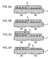
- FIG. 5A shows the insulating film 3 similar to FIG. 3A except the frequency of the first surface acoustic wave element is lower than the desired value. That is, the film-thickness of the insulating film 3 of FIG. 5A is thicker than the insulating film 3 shown in FIG. 3A.
- the frequency characteristic of the first surface acoustic wave element 30 is measured by wafer probing.
- the adjustment amount of the frequency characteristic is determined based on the measurement results.
- the surface of the insulating film 3 is plasma-etched so that the frequency of the first surface acoustic wave element 30 has a desired value.
- the thickness of the insulating film 3 is set at a predetermined value so that the frequency characteristic of the first surface acoustic wave element 30 has this desired value.
- the frequency characteristic of the second surface acoustic wave element 40 is measured by wafer probing, and the adjustment amount of the frequency characteristic is determined based on the measurement results.
- a positive resist is applied to the whole surface of the insulating film 3 shown in FIG. 5B.
- the resist is exposed through a mask having a shielding portion corresponding to the first surface acoustic wave element 30. Then, the exposed resist part is removed to obtain a patterned resist 2a shown in FIG. 5C.
- etching is performed using an etchant which is capable of removing the insulating film 3 but not the resist 2a, and subsequently, a step 3x is produced on the insulating film 3 as shown in FIG. 5D.
- the etching may be of wet type or dry type using plasma or other suitable methods.
- the number of defective composite elements is minimized by applying the SiO 2 film on the first and second surface acoustic wave elements. Since the SiO 2 film formed on the second surface acoustic wave element is adjusted after the SiO 2 film formed on the first surface acoustic wave element is adjusted, the frequencies of the two surface acoustic wave elements are effectively adjusted. The number of defective composite elements is minimized.
- the technique in which the insulating films formed on the first and second surface acoustic wave elements are made different from each other so that the frequencies of the two different surface acoustic wave elements are effectively adjusted can be used for the one terminal pair resonator described in the first preferred embodiment.
- the techniques described in the first to third preferred embodiments of the present invention can be applied to any suitable device, such as a resonator, a filter, a duplexer or other electronic component.
- the techniques can also be applied to surface acoustic wave elements having no reflectors.
- the thickness of the conductive film of the second surface acoustic wave element is preferably less than that of the conductive film of the first surface acoustic wave element. Conversely, the thickness of the conductive film of the second surface acoustic wave element may be greater than that of the conductive film of the first surface acoustic wave element.
- the piezoelectric substrate in the respective preferred embodiments can be any suitable piezoelectric single crystals such as quartz, lithium tetraborate, and langasite, and any suitable piezoelectric ceramics such as lead titanate zirconate-type piezoelectric ceramic. Further, piezoelectric substrates having piezoelectric thin films made of ZnO or other suitable thin films, formed on insulation substrates made of alumina or other suitable insulation substrates may be used. As electrode material for the IDT, the reflectors, and other elements, any of A1, A1 alloys, and other conductive materials can be applied for the present invention. Moreover, the insulating film for adjusting the frequency characteristic is not limited to SiO 2 .
Landscapes
- Physics & Mathematics (AREA)
- Acoustics & Sound (AREA)
- Engineering & Computer Science (AREA)
- Manufacturing & Machinery (AREA)
- Surface Acoustic Wave Elements And Circuit Networks Thereof (AREA)
Claims (4)
- Procédé de production d'un dispositif à ondes acoustiques de surface comportant des premier et second éléments à ondes acoustiques de surface (10, 20) disposés sur un substrat piézoélectrique (1), comprenant les étapes consistant à :former un transducteur interdigité (11) du premier élément à ondes acoustiques de surface (10) sur le substrat piézoélectrique, le transducteur interdigité (11) comportant des bornes d'entrée-sortie électriquement reliées via une électrode de court-circuit (15) ;disposer un résist (2) sur toute la surface du substrat (1) où le transducteur interdigité (11) du premier élément à ondes acoustiques de surface (10) et l'électrode de court-circuit (15) sont formés ;chauffer le résist (2) ;retirer le résist seulement de la zone où le second élément à ondes acoustiques de surface (20) sera formé ;appliquer un film conducteur sur le substrat piézoélectrique (1), le film conducteur ayant une épaisseur qui est différente d'une épaisseur du transducteur interdigité (11) du premier élément à ondes acoustiques de surface (10) ;modeler le film conducteur pour former un transducteur interdigité (21) du second élément à ondes acoustiques de surface (20) ;couper l'électrode de court-circuit (15) pour déconnecter électriquement les bornes d'entrée-sortie du transducteur interdigité (11) du premier élément à ondes acoustiques de surface (10) ;former un film isolant (3) sur les transducteurs interdigités (11, 21) des premier et second éléments à ondes acoustiques de surface (10, 20) ; etdiminuer l'épaisseur du film isolant (3) pour ajuster les caractéristiques de fréquence d'au moins un élément parmi les premier et second éléments à ondes acoustiques de surface (10, 20).
- Procédé de production d'un dispositif à ondes acoustiques de surface selon la revendication 1, comprenant en outre l'étape consistant à mesurer les caractéristiques de fréquence des premier et second éléments à ondes acoustiques de surface (10, 20) par sondage de plaquette avant l'étape consistant à ajuster les caractéristiques de fréquence ;
dans lequel l'étape consistant à diminuer l'épaisseur du film isolant (3) est effectuée de sorte que l'épaisseur du film isolant au niveau d'une région sur le transducteur interdigité (11) du premier élément à ondes acoustiques de surface (10) soit différente de l'épaisseur du film isolant au niveau d'une région sur le transducteur interdigité (21) du second élément à ondes acoustiques de surface (20), après l'étape consistant à former le film isolant (3). - Procédé de production d'un dispositif à ondes acoustiques de surface selon la revendication 2, dans lequel l'étape consistant à diminuer l'épaisseur du film isolant (3) comprend les étapes consistant à diminuer l'épaisseur de tout le film isolant de sorte qu'un (30) des premier et second éléments à ondes acoustiques de surface (30, 40) ait une caractéristique de fréquence souhaitée, mesurer les caractéristiques de fréquence de l'autre (40) des premier et second éléments à ondes acoustiques de surface pour déterminer l'épaisseur souhaitée du film isolant (3) pour l'autre (40) des premier et second éléments à ondes acoustiques de surface afin d'obtenir les caractéristiques de fréquence souhaitées, et diminuer l'épaisseur du film isolant (3) seulement sur une région de l'autre (40) des premier et second éléments à ondes acoustiques de surface pour avoir une caractéristique de fréquence souhaitée sur la base de l'épaisseur souhaitée déterminée par l'étape de mesure.
- Procédé de production d'un dispositif à ondes acoustiques de surface selon la revendication 2, dans lequel, dans l'étape consistant à former le transducteur interdigité du premier élément à ondes acoustiques de surface (30) et l'étape consistant à former le transducteur interdigité du second élément à ondes acoustiques de surface (40), les transducteurs interdigités sont formés de sorte que la fréquence de chaque élément parmi le premier élément à ondes acoustiques de surface (30) et le second élément à ondes acoustiques de surface (40) est supérieure à une fréquence prédéterminée ; et dans l'étape consistant à former le film isolant (3), le film isolant (3) est formé de sorte que la fréquence de chaque élément parmi le premier élément à ondes acoustiques de surface (30) et le second élément à ondes acoustiques de surface (40) devienne inférieure à la fréquence prédéterminée ; le procédé comprenant en outre l'étape consistant à graver le film isolant (3) au niveau de la région sur le premier élément à ondes acoustiques de surface (30) et le film isolant (3) au niveau de la région sur le second élément à ondes acoustiques de surface (40) simultanément de sorte que la fréquence d'un (30) des premier et second éléments à ondes acoustiques de surface (30, 40) augmente à une valeur souhaitée ; la fréquence de l'autre (40) des premier et second éléments à ondes acoustiques de surface (30, 40) est mesurée par sondage de plaquette, et seul le film isolant (3) au niveau de la région sur l'autre (40) des premier et second éléments à ondes acoustiques de surface (30, 40) est gravé par plasma de sorte que la fréquence de l'autre des premier et second éléments à ondes acoustiques de surface augmente à une valeur souhaitée.
Applications Claiming Priority (2)
| Application Number | Priority Date | Filing Date | Title |
|---|---|---|---|
| JP14680099 | 1999-05-26 | ||
| JP14680099A JP3317274B2 (ja) | 1999-05-26 | 1999-05-26 | 弾性表面波装置及び弾性表面波装置の製造方法 |
Publications (4)
| Publication Number | Publication Date |
|---|---|
| EP1056202A2 EP1056202A2 (fr) | 2000-11-29 |
| EP1056202A3 EP1056202A3 (fr) | 2003-03-26 |
| EP1056202B1 true EP1056202B1 (fr) | 2007-08-22 |
| EP1056202B8 EP1056202B8 (fr) | 2007-10-10 |
Family
ID=15415826
Family Applications (1)
| Application Number | Title | Priority Date | Filing Date |
|---|---|---|---|
| EP00401484A Expired - Lifetime EP1056202B8 (fr) | 1999-05-26 | 2000-05-26 | Procédé pour la fabrication d'un dispositif à ondes acoustiques de surface |
Country Status (6)
| Country | Link |
|---|---|
| US (2) | US6516503B1 (fr) |
| EP (1) | EP1056202B8 (fr) |
| JP (1) | JP3317274B2 (fr) |
| KR (1) | KR100560067B1 (fr) |
| CN (1) | CN1173467C (fr) |
| DE (1) | DE60036050D1 (fr) |
Families Citing this family (149)
| Publication number | Priority date | Publication date | Assignee | Title |
|---|---|---|---|---|
| JP3317274B2 (ja) * | 1999-05-26 | 2002-08-26 | 株式会社村田製作所 | 弾性表面波装置及び弾性表面波装置の製造方法 |
| JP3925133B2 (ja) * | 2000-12-26 | 2007-06-06 | 株式会社村田製作所 | 弾性表面波装置の製造方法及び弾性表面波装置 |
| JP3801083B2 (ja) * | 2001-06-06 | 2006-07-26 | 株式会社村田製作所 | 弾性表面波装置 |
| TWI315607B (en) * | 2001-10-29 | 2009-10-01 | Panasonic Corp | Surface acoustic wave filter element, surface acoustic wave filter and communication device using the same |
| JP4166997B2 (ja) * | 2002-03-29 | 2008-10-15 | 富士通メディアデバイス株式会社 | 弾性表面波素子の実装方法及び樹脂封止された弾性表面波素子を有する弾性表面波装置 |
| WO2005088835A1 (fr) * | 2004-03-12 | 2005-09-22 | Murata Manufacturing Co., Ltd. | Demultiplexeur et filtre a ondes acoustiques de surface |
| DE102004037819B4 (de) * | 2004-08-04 | 2021-12-16 | Snaptrack, Inc. | Elektroakustisches Bauelement mit geringen Verlusten |
| JP2007202087A (ja) * | 2005-05-11 | 2007-08-09 | Seiko Epson Corp | ラム波型高周波デバイス |
| JP2007110342A (ja) * | 2005-10-12 | 2007-04-26 | Kyocera Corp | 弾性表面波素子及びその製造方法 |
| JP4917396B2 (ja) * | 2006-09-25 | 2012-04-18 | 太陽誘電株式会社 | フィルタおよび分波器 |
| JP4521451B2 (ja) * | 2008-03-24 | 2010-08-11 | 富士通メディアデバイス株式会社 | 弾性表面波デバイス及びその製造方法 |
| JP5339582B2 (ja) | 2008-07-31 | 2013-11-13 | 太陽誘電株式会社 | 弾性波デバイス |
| US8258674B2 (en) * | 2008-11-03 | 2012-09-04 | Viorel Olariu | Surface acoustic wave sensor and system |
| JP4841640B2 (ja) * | 2009-03-25 | 2011-12-21 | 太陽誘電株式会社 | 弾性波デバイスおよびその製造方法 |
| CN104734662B (zh) * | 2009-04-22 | 2017-09-22 | 天工滤波方案日本有限公司 | 弹性波元件和使用它的电子设备 |
| CN101923657B (zh) * | 2010-08-11 | 2012-11-07 | 上海交通大学 | 具有数据纠错功能的声表面波射频标签及其纠错方法 |
| JP5766457B2 (ja) * | 2011-02-09 | 2015-08-19 | 太陽誘電株式会社 | 弾性波デバイス及びその製造方法 |
| JP5672050B2 (ja) * | 2011-02-21 | 2015-02-18 | 株式会社村田製作所 | 弾性表面波フィルタ装置 |
| WO2015022931A1 (fr) * | 2013-08-14 | 2015-02-19 | 株式会社村田製作所 | Dispositif à ondes élastiques, composant électronique et méthode de fabrication de dispositif à ondes élastiques |
| US9634644B2 (en) * | 2014-07-28 | 2017-04-25 | Skyworks Filter Solutions Japan Co., Ltd. | Acoustic wave elements and antenna duplexers, and modules and electronic devices using same |
| JP2017522822A (ja) | 2014-07-28 | 2017-08-10 | スカイワークスフィルターソリューションズジャパン株式会社 | 弾性波素子、アンテナデュプレクサ、モジュール及びこれらを使用する電子機器 |
| US9641151B2 (en) * | 2014-07-31 | 2017-05-02 | Skyworks Filter Solutions Japan Co., Ltd. | Elastic wave filters and duplexers using same |
| CN106664072A (zh) * | 2014-07-31 | 2017-05-10 | 天工滤波方案日本有限公司 | 声波滤波器和使用其的双工器 |
| CN107112968B (zh) * | 2015-01-22 | 2020-10-16 | 株式会社村田制作所 | 弹性波装置的制造方法以及弹性波装置 |
| JP6390819B2 (ja) | 2016-04-25 | 2018-09-19 | 株式会社村田製作所 | 弾性波装置及びその製造方法 |
| US10187039B2 (en) * | 2016-06-07 | 2019-01-22 | Skyworks Filter Solutions Japan Co., Ltd. | Filter devices having reduced spurious emissions from lamb waves |
| CN109643982B (zh) | 2016-08-30 | 2020-03-24 | 株式会社村田制作所 | 弹性波装置及其制造方法 |
| CN110063024B (zh) * | 2016-10-11 | 2024-01-19 | 京瓷株式会社 | 弹性波装置 |
| CN106656098B (zh) * | 2016-12-23 | 2020-11-24 | 无锡市好达电子有限公司 | 一种超大带宽声表面波滤波器 |
| KR102290082B1 (ko) * | 2017-02-28 | 2021-08-17 | 가부시키가이샤 무라타 세이사쿠쇼 | 탄성파 장치 및 그 제조 방법 |
| US11509279B2 (en) | 2020-07-18 | 2022-11-22 | Resonant Inc. | Acoustic resonators and filters with reduced temperature coefficient of frequency |
| US11929731B2 (en) | 2018-02-18 | 2024-03-12 | Murata Manufacturing Co., Ltd. | Transversely-excited film bulk acoustic resonator with optimized electrode mark, and pitch |
| US10601392B2 (en) | 2018-06-15 | 2020-03-24 | Resonant Inc. | Solidly-mounted transversely-excited film bulk acoustic resonator |
| US11206009B2 (en) | 2019-08-28 | 2021-12-21 | Resonant Inc. | Transversely-excited film bulk acoustic resonator with interdigital transducer with varied mark and pitch |
| US12237826B2 (en) | 2018-06-15 | 2025-02-25 | Murata Manufacturing Co., Ltd. | Transversely-excited film bulk acoustic resonator with optimized electrode thickness, mark, and pitch |
| US10790802B2 (en) | 2018-06-15 | 2020-09-29 | Resonant Inc. | Transversely excited film bulk acoustic resonator using rotated Y-X cut lithium niobate |
| US11323089B2 (en) | 2018-06-15 | 2022-05-03 | Resonant Inc. | Filter using piezoelectric film bonded to high resistivity silicon substrate with trap-rich layer |
| US10491192B1 (en) * | 2018-06-15 | 2019-11-26 | Resonant Inc. | Transversely-excited film bulk acoustic resonator |
| US11146232B2 (en) | 2018-06-15 | 2021-10-12 | Resonant Inc. | Transversely-excited film bulk acoustic resonator with reduced spurious modes |
| US12040779B2 (en) | 2020-04-20 | 2024-07-16 | Murata Manufacturing Co., Ltd. | Small transversely-excited film bulk acoustic resonators with enhanced Q-factor |
| US11936358B2 (en) | 2020-11-11 | 2024-03-19 | Murata Manufacturing Co., Ltd. | Transversely-excited film bulk acoustic resonator with low thermal impedance |
| US10756697B2 (en) | 2018-06-15 | 2020-08-25 | Resonant Inc. | Transversely-excited film bulk acoustic resonator |
| US11323096B2 (en) | 2018-06-15 | 2022-05-03 | Resonant Inc. | Transversely-excited film bulk acoustic resonator with periodic etched holes |
| US11323090B2 (en) | 2018-06-15 | 2022-05-03 | Resonant Inc. | Transversely-excited film bulk acoustic resonator using Y-X-cut lithium niobate for high power applications |
| US10637438B2 (en) | 2018-06-15 | 2020-04-28 | Resonant Inc. | Transversely-excited film bulk acoustic resonators for high power applications |
| US12088281B2 (en) | 2021-02-03 | 2024-09-10 | Murata Manufacturing Co., Ltd. | Transversely-excited film bulk acoustic resonator with multi-mark interdigital transducer |
| DE102018109974B3 (de) * | 2018-04-25 | 2019-09-12 | RF360 Europe GmbH | Elektroakustisches Filter, Multiplexer und Verfahren zur Herstellung eines elektroakustischen Filters |
| US11996822B2 (en) | 2018-06-15 | 2024-05-28 | Murata Manufacturing Co., Ltd. | Wide bandwidth time division duplex transceiver |
| US11329628B2 (en) | 2020-06-17 | 2022-05-10 | Resonant Inc. | Filter using lithium niobate and lithium tantalate transversely-excited film bulk acoustic resonators |
| US10819309B1 (en) | 2019-04-05 | 2020-10-27 | Resonant Inc. | Transversely-excited film bulk acoustic resonator package and method |
| US11374549B2 (en) | 2018-06-15 | 2022-06-28 | Resonant Inc. | Filter using transversely-excited film bulk acoustic resonators with divided frequency-setting dielectric layers |
| US11323095B2 (en) | 2018-06-15 | 2022-05-03 | Resonant Inc. | Rotation in XY plane to suppress spurious modes in XBAR devices |
| US11349450B2 (en) | 2018-06-15 | 2022-05-31 | Resonant Inc. | Symmetric transversely-excited film bulk acoustic resonators with reduced spurious modes |
| US11888463B2 (en) | 2018-06-15 | 2024-01-30 | Murata Manufacturing Co., Ltd. | Multi-port filter using transversely-excited film bulk acoustic resonators |
| US12184261B2 (en) | 2018-06-15 | 2024-12-31 | Murata Manufacturing Co., Ltd. | Transversely-excited film bulk acoustic resonator with a cavity having round end zones |
| US12191838B2 (en) | 2018-06-15 | 2025-01-07 | Murata Manufacturing Co., Ltd. | Solidly-mounted transversely-excited film bulk acoustic device and method |
| US11323091B2 (en) | 2018-06-15 | 2022-05-03 | Resonant Inc. | Transversely-excited film bulk acoustic resonator with diaphragm support pedestals |
| US11916539B2 (en) | 2020-02-28 | 2024-02-27 | Murata Manufacturing Co., Ltd. | Split-ladder band N77 filter using transversely-excited film bulk acoustic resonators |
| US11349452B2 (en) | 2018-06-15 | 2022-05-31 | Resonant Inc. | Transversely-excited film bulk acoustic filters with symmetric layout |
| US11728785B2 (en) | 2018-06-15 | 2023-08-15 | Murata Manufacturing Co., Ltd. | Transversely-excited film bulk acoustic resonator using pre-formed cavities |
| US11876498B2 (en) | 2018-06-15 | 2024-01-16 | Murata Manufacturing Co., Ltd. | Transversely-excited film bulk acoustic resonator with multiple diaphragm thicknesses and fabrication method |
| US11949402B2 (en) | 2020-08-31 | 2024-04-02 | Murata Manufacturing Co., Ltd. | Resonators with different membrane thicknesses on the same die |
| US12463619B2 (en) | 2018-06-15 | 2025-11-04 | Murata Manufacturing Co., Ltd. | Filter device |
| US11901878B2 (en) | 2018-06-15 | 2024-02-13 | Murata Manufacturing Co., Ltd. | Transversely-excited film bulk acoustic resonators with two-layer electrodes with a wider top layer |
| US12119808B2 (en) | 2018-06-15 | 2024-10-15 | Murata Manufacturing Co., Ltd. | Transversely-excited film bulk acoustic resonator package |
| US11228296B2 (en) | 2018-06-15 | 2022-01-18 | Resonant Inc. | Transversely-excited film bulk acoustic resonator with a cavity having a curved perimeter |
| US12040781B2 (en) | 2018-06-15 | 2024-07-16 | Murata Manufacturing Co., Ltd. | Transversely-excited film bulk acoustic resonator package |
| US11146238B2 (en) | 2018-06-15 | 2021-10-12 | Resonant Inc. | Film bulk acoustic resonator fabrication method |
| US11909381B2 (en) | 2018-06-15 | 2024-02-20 | Murata Manufacturing Co., Ltd. | Transversely-excited film bulk acoustic resonators with two-layer electrodes having a narrower top layer |
| US12237827B2 (en) | 2018-06-15 | 2025-02-25 | Murata Manufacturing Co., Ltd. | Solidly-mounted transversely-excited film bulk acoustic filters with multiple piezoelectric plate thicknesses |
| US12119805B2 (en) | 2018-06-15 | 2024-10-15 | Murata Manufacturing Co., Ltd. | Substrate processing and membrane release of transversely-excited film bulk acoustic resonator using a sacrificial tub |
| US12224732B2 (en) | 2018-06-15 | 2025-02-11 | Murata Manufacturing Co., Ltd. | Solidly-mounted transversely-excited film bulk acoustic resonators and filters for 27 GHz communications bands |
| US12081187B2 (en) | 2018-06-15 | 2024-09-03 | Murata Manufacturing Co., Ltd. | Transversely-excited film bulk acoustic resonator |
| US11264966B2 (en) | 2018-06-15 | 2022-03-01 | Resonant Inc. | Solidly-mounted transversely-excited film bulk acoustic resonator with diamond layers in Bragg reflector stack |
| US11201601B2 (en) | 2018-06-15 | 2021-12-14 | Resonant Inc. | Transversely-excited film bulk acoustic resonator with multiple diaphragm thicknesses and fabrication method |
| US12212306B2 (en) | 2018-06-15 | 2025-01-28 | Murata Manufacturing Co., Ltd. | Transversely-excited film bulk acoustic resonator with multiple diaphragm thicknesses and fabrication method |
| US12113512B2 (en) | 2021-03-29 | 2024-10-08 | Murata Manufacturing Co., Ltd. | Layout of XBARs with multiple sub-resonators in parallel |
| US10917072B2 (en) | 2019-06-24 | 2021-02-09 | Resonant Inc. | Split ladder acoustic wave filters |
| US12155374B2 (en) | 2021-04-02 | 2024-11-26 | Murata Manufacturing Co., Ltd. | Tiled transversely-excited film bulk acoustic resonator high power filters |
| US12155371B2 (en) | 2021-03-29 | 2024-11-26 | Murata Manufacturing Co., Ltd. | Layout of xbars with multiple sub-resonators in series |
| US11967945B2 (en) | 2018-06-15 | 2024-04-23 | Murata Manufacturing Co., Ltd. | Transversly-excited film bulk acoustic resonators and filters |
| US12191837B2 (en) | 2018-06-15 | 2025-01-07 | Murata Manufacturing Co., Ltd. | Solidly-mounted transversely-excited film bulk acoustic device |
| US10826462B2 (en) | 2018-06-15 | 2020-11-03 | Resonant Inc. | Transversely-excited film bulk acoustic resonators with molybdenum conductors |
| US11171629B2 (en) | 2018-06-15 | 2021-11-09 | Resonant Inc. | Transversely-excited film bulk acoustic resonator using pre-formed cavities |
| US12149227B2 (en) | 2018-06-15 | 2024-11-19 | Murata Manufacturing Co., Ltd. | Transversely-excited film bulk acoustic resonator package |
| US12009798B2 (en) | 2018-06-15 | 2024-06-11 | Murata Manufacturing Co., Ltd. | Transversely-excited film bulk acoustic resonators with electrodes having irregular hexagon cross-sectional shapes |
| US10998877B2 (en) * | 2018-06-15 | 2021-05-04 | Resonant Inc. | Film bulk acoustic resonator fabrication method with frequency trimming based on electric measurements prior to cavity etch |
| US11901873B2 (en) | 2019-03-14 | 2024-02-13 | Murata Manufacturing Co., Ltd. | Transversely-excited film bulk acoustic resonator with partial BRAGG reflectors |
| CN113615083B (zh) | 2019-03-14 | 2024-10-15 | 株式会社村田制作所 | 带有半λ介电层的横向激励的薄膜体声学谐振器 |
| US12034423B2 (en) | 2019-06-27 | 2024-07-09 | Murata Manufacturing Co., Ltd | XBAR frontside etch process using polysilicon sacrificial layer |
| US10911021B2 (en) | 2019-06-27 | 2021-02-02 | Resonant Inc. | Transversely-excited film bulk acoustic resonator with lateral etch stop |
| CN110429917A (zh) * | 2019-08-09 | 2019-11-08 | 宜确半导体(苏州)有限公司 | 声表面波滤波器及其制造方法 |
| US12506462B2 (en) | 2020-02-28 | 2025-12-23 | Murata Manufacturing Co., Ltd. | Transversely-excited film bulk acoustic resonator with multi-pitch interdigital transducer |
| US12255625B2 (en) | 2020-02-28 | 2025-03-18 | Murata Manufacturing Co., Ltd. | Filter using transversely-excited film bulk acoustic resonators with inductively coupled sub-resonators |
| US12341490B2 (en) | 2020-04-20 | 2025-06-24 | Murata Manufacturing Co., Ltd. | Low loss transversely-excited film bulk acoustic resonators and filters |
| US12341493B2 (en) | 2020-04-20 | 2025-06-24 | Murata Manufacturing Co., Ltd. | Low loss transversely-excited film bulk acoustic resonators and filters |
| US12278617B2 (en) | 2020-04-20 | 2025-04-15 | Murata Manufacturing Co., Ltd. | High Q solidly-mounted transversely-excited film bulk acoustic resonators |
| US11811391B2 (en) | 2020-05-04 | 2023-11-07 | Murata Manufacturing Co., Ltd. | Transversely-excited film bulk acoustic resonator with etched conductor patterns |
| US11469733B2 (en) | 2020-05-06 | 2022-10-11 | Resonant Inc. | Transversely-excited film bulk acoustic resonators with interdigital transducer configured to reduce diaphragm stress |
| US12074584B2 (en) | 2020-05-28 | 2024-08-27 | Murata Manufacturing Co., Ltd. | Transversely-excited film bulk acoustic resonators with two-layer electrodes |
| US12267062B2 (en) | 2020-06-17 | 2025-04-01 | Murata Manufacturing Co., Ltd. | Transversely-excited film bulk acoustic resonators with three-layer electrodes |
| US11482981B2 (en) | 2020-07-09 | 2022-10-25 | Resonanat Inc. | Transversely-excited film bulk acoustic resonators with piezoelectric diaphragm supported by piezoelectric substrate |
| US11264969B1 (en) | 2020-08-06 | 2022-03-01 | Resonant Inc. | Transversely-excited film bulk acoustic resonator comprising small cells |
| US11271539B1 (en) | 2020-08-19 | 2022-03-08 | Resonant Inc. | Transversely-excited film bulk acoustic resonator with tether-supported diaphragm |
| US11671070B2 (en) | 2020-08-19 | 2023-06-06 | Murata Manufacturing Co., Ltd. | Transversely-excited film bulk acoustic resonators using multiple dielectric layer thicknesses to suppress spurious modes |
| US11894835B2 (en) | 2020-09-21 | 2024-02-06 | Murata Manufacturing Co., Ltd. | Sandwiched XBAR for third harmonic operation |
| US11929733B2 (en) | 2020-10-05 | 2024-03-12 | Murata Manufacturing Co., Ltd. | Transversely-excited film bulk acoustic resonator matrix filters with input and output impedances matched to radio frequency front end elements |
| US11658639B2 (en) | 2020-10-05 | 2023-05-23 | Murata Manufacturing Co., Ltd. | Transversely-excited film bulk acoustic resonator matrix filters with noncontiguous passband |
| US11728784B2 (en) | 2020-10-05 | 2023-08-15 | Murata Manufacturing Co., Ltd. | Transversely-excited film bulk acoustic resonator matrix filters with split die sub-filters |
| US11476834B2 (en) | 2020-10-05 | 2022-10-18 | Resonant Inc. | Transversely-excited film bulk acoustic resonator matrix filters with switches in parallel with sub-filter shunt capacitors |
| US11405017B2 (en) | 2020-10-05 | 2022-08-02 | Resonant Inc. | Acoustic matrix filters and radios using acoustic matrix filters |
| US12119806B2 (en) | 2020-10-30 | 2024-10-15 | Murata Manufacturing Co., Ltd. | Transversely-excited film bulk acoustic resonator with spiral interdigitated transducer fingers |
| US12255617B2 (en) | 2020-11-11 | 2025-03-18 | Murata Manufacturing Co., Ltd. | Solidly-mounted transversely-excited film bulk acoustic resonators with low thermal impedance |
| US12003226B2 (en) | 2020-11-11 | 2024-06-04 | Murata Manufacturing Co., Ltd | Transversely-excited film bulk acoustic resonator with low thermal impedance |
| US12431856B2 (en) | 2020-11-12 | 2025-09-30 | Murata Manufacturing Co., Ltd. | Transversely-excited film bulk acoustic resonator with reduced loss in the aperture direction |
| US11496113B2 (en) | 2020-11-13 | 2022-11-08 | Resonant Inc. | XBAR devices with excess piezoelectric material removed |
| US12255626B2 (en) | 2020-11-13 | 2025-03-18 | Murata Manufacturing Co., Ltd. | Solidly-mounted transversely-excited film bulk acoustic filters with excess piezoelectric material removed |
| US20230412142A1 (en) * | 2020-11-16 | 2023-12-21 | Qorvo Us, Inc. | Piezoelectric layer arrangements in acoustic wave devices and related methods |
| US11405020B2 (en) | 2020-11-26 | 2022-08-02 | Resonant Inc. | Transversely-excited film bulk acoustic resonators with structures to reduce acoustic energy leakage |
| US11239816B1 (en) | 2021-01-15 | 2022-02-01 | Resonant Inc. | Decoupled transversely-excited film bulk acoustic resonators |
| US12126318B2 (en) | 2021-01-15 | 2024-10-22 | Murata Manufacturing Co., Ltd. | Filters using decoupled transversely-excited film bulk acoustic resonators |
| US12463615B2 (en) | 2021-01-21 | 2025-11-04 | Murata Manufacturing Co., Ltd | Transversely-excited film bulk acoustic resonators with improved coupling and reduced energy leakage |
| US12113510B2 (en) | 2021-02-03 | 2024-10-08 | Murata Manufacturing Co., Ltd. | Transversely-excited film bulk acoustic resonators with multiple piezoelectric membrane thicknesses on the same chip |
| US12308826B2 (en) | 2021-02-03 | 2025-05-20 | Murata Manufacturing Co., Ltd. | Bandpass filters using transversely-excited film bulk acoustic resonators |
| US12308825B2 (en) | 2021-02-12 | 2025-05-20 | Murata Manufacturing Co., Ltd | Transversely-excited film bulk acoustic resonators with narrow gaps between busbars and ends of interdigital transducer fingers |
| US12355426B2 (en) | 2021-03-24 | 2025-07-08 | Murata Manufacturing Co., Ltd. | Acoustic filters with shared acoustic tracks |
| US12126328B2 (en) | 2021-03-24 | 2024-10-22 | Murata Manufacturing Co., Ltd. | Acoustic filters with shared acoustic tracks |
| US12289099B2 (en) | 2021-03-24 | 2025-04-29 | Murata Manufacturing Co., Ltd. | Acoustic filters with shared acoustic tracks for series and shunt resonators |
| US12348216B2 (en) | 2021-03-24 | 2025-07-01 | Murata Manufacturing Co., Ltd. | Acoustic filters with shared acoustic tracks and cascaded series resonators |
| US12341492B2 (en) | 2021-03-29 | 2025-06-24 | Murata Manufacturing Co., Ltd. | Transversely-excited film bulk acoustic resonators with busbar side edges that form angles with a perimeter of the cavity |
| US12224735B2 (en) | 2021-03-30 | 2025-02-11 | Murata Manufacturing Co., Ltd. | Diplexer using decoupled transversely-excited film bulk acoustic resonators |
| CN120454674A (zh) | 2021-03-30 | 2025-08-08 | 株式会社村田制作所 | 使用横向激发薄膜体声谐振器的用于6 GHz WI-FI的滤波器 |
| US12249971B2 (en) | 2021-04-02 | 2025-03-11 | Murata Manufacturing Co., Ltd. | Transversely-excited film bulk acoustic resonators with solidly mounted resonator (SMR) pedestals |
| US12237823B2 (en) | 2021-04-02 | 2025-02-25 | Murata Manufacturing Co., Ltd. | Transversely-excited film bulk acoustic resonators with solidly mounted resonator (SMR) pedestals |
| US12126316B2 (en) | 2021-04-16 | 2024-10-22 | Murata Manufacturing Co., Ltd | Transversely-excited film bulk acoustic resonator |
| US12255633B2 (en) | 2021-04-16 | 2025-03-18 | Murata Manufacturing Co., Ltd. | Filter using transversely-excited film bulk acoustic resonators |
| US12255607B2 (en) | 2021-04-30 | 2025-03-18 | Murata Manufacturing Co., Ltd. | Transversely-excited film bulk acoustic resonator with buried oxide strip acoustic confinement structures |
| US12160220B2 (en) | 2021-04-30 | 2024-12-03 | Murata Manufacturing Co., Ltd. | Transversely-excited film bulk acoustic resonator with oxide strip acoustic confinement structures |
| US12075700B2 (en) | 2021-05-07 | 2024-08-27 | Murata Manufacturing Co., Ltd. | Transversely-excited film bulk acoustic resonator fabrication using polysilicon pillars |
| US12057823B2 (en) | 2021-05-07 | 2024-08-06 | Murata Manufacturing Co., Ltd. | Transversely-excited film bulk acoustic resonator with concentric interdigitated transducer fingers |
| US12170513B2 (en) | 2021-06-30 | 2024-12-17 | Murata Manufacturing Co., Ltd. | Transversely-excited film bulk acoustic resonator with reduced substrate to contact bump thermal resistance |
| US12603639B2 (en) | 2021-08-02 | 2026-04-14 | Murata Manufacturing Co., Ltd. | Metal cavity for transversely-excited film bulk acoustic resonator (XBAR) |
| CN113810014B (zh) * | 2021-09-23 | 2025-08-22 | 武汉敏声新技术有限公司 | 叉指型体声波谐振器及滤波器 |
| US12456962B2 (en) | 2021-09-24 | 2025-10-28 | Murata Manufacturing Co., Ltd. | Transversely-excited film bulk acoustic resonators wafer-level packaging using a dielectric cover |
| US12451864B2 (en) | 2021-09-29 | 2025-10-21 | Murata Manufacturing Co., Ltd. | Transversely-excited film bulk acoustic resonators with curved shaped ends of fingers or opposing busbars |
| US12225387B2 (en) | 2021-09-29 | 2025-02-11 | Murata Manufacturing Co., Ltd. | Communications device with concurrent operation in 5GHZ and 6GHZ U-NII frequency ranges |
| US12407326B2 (en) | 2021-11-04 | 2025-09-02 | Murata Manufacturing Co., Ltd. | Stacked die transversely-excited film bulk acoustic resonator (XBAR) filters |
| CN114094981B (zh) * | 2021-11-12 | 2025-03-04 | 北京超材信息科技有限公司 | 一种双声表面波滤波器、双频组件及其制造方法 |
| TWI802380B (zh) | 2022-04-21 | 2023-05-11 | 立積電子股份有限公司 | 聲波裝置及其製造方法 |
Family Cites Families (18)
| Publication number | Priority date | Publication date | Assignee | Title |
|---|---|---|---|---|
| US4243960A (en) * | 1978-08-14 | 1981-01-06 | The United States Of America As Represented By The Secretary Of The Navy | Method and materials for tuning the center frequency of narrow-band surface-acoustic-wave (SAW) devices by means of dielectric overlays |
| US4442574A (en) * | 1982-07-26 | 1984-04-17 | General Electric Company | Frequency trimming of saw resonators |
| KR920005610B1 (ko) * | 1985-04-11 | 1992-07-09 | 도오요오 쓰으신끼 가부시끼가이샤 | 오버톤 발진용 압전 공진자 |
| JPS6247206A (ja) * | 1985-08-27 | 1987-02-28 | Nec Corp | 弾性表面波多重モ−ドフイルタ |
| JPH0326013A (ja) | 1989-06-22 | 1991-02-04 | Murata Mfg Co Ltd | 弾性表面波フィルター |
| CA2038474C (fr) * | 1990-03-19 | 1994-09-20 | Yoshio Satoh | Filtre a ondes acoustiques de surface comportant plusieurs electrodes |
| JPH0590872A (ja) * | 1991-09-27 | 1993-04-09 | Sumitomo Electric Ind Ltd | 表面弾性波素子 |
| US5221870A (en) * | 1991-09-30 | 1993-06-22 | Sumitomo Electric Industries, Ltd. | Surface acoustic wave device |
| JP3163606B2 (ja) | 1993-01-29 | 2001-05-08 | 住友電気工業株式会社 | 表面弾性波素子 |
| WO1995002279A1 (fr) | 1993-07-06 | 1995-01-19 | Motorola, Inc. | Dispositif a ondes acoustiques de surface |
| US5815900A (en) * | 1995-03-06 | 1998-10-06 | Matsushita Electric Industrial Co., Ltd. | Method of manufacturing a surface acoustic wave module |
| JP3189719B2 (ja) | 1996-12-25 | 2001-07-16 | 株式会社村田製作所 | 弾性表面波装置の製造方法 |
| JPH10303680A (ja) * | 1997-04-25 | 1998-11-13 | Nec Corp | 弾性表面波フィルタ |
| EP0920129B1 (fr) * | 1997-05-08 | 2006-12-27 | Kabushiki Kaisha Toshiba | Dispositif a ondes limites elastiques et son procede de fabrication |
| JP3171144B2 (ja) * | 1997-07-07 | 2001-05-28 | 株式会社村田製作所 | 表面波装置 |
| WO1999005788A1 (fr) * | 1997-07-28 | 1999-02-04 | Kabushiki Kaisha Toshiba | Dispositif de traitement d'ondes acoustiques de surface et son procede de fabrication |
| JPH11163655A (ja) * | 1997-12-01 | 1999-06-18 | Murata Mfg Co Ltd | 弾性表面波装置の製造方法 |
| JP3317274B2 (ja) * | 1999-05-26 | 2002-08-26 | 株式会社村田製作所 | 弾性表面波装置及び弾性表面波装置の製造方法 |
-
1999
- 1999-05-26 JP JP14680099A patent/JP3317274B2/ja not_active Expired - Fee Related
-
2000
- 2000-05-18 KR KR1020000026668A patent/KR100560067B1/ko not_active Expired - Fee Related
- 2000-05-19 US US09/574,794 patent/US6516503B1/en not_active Expired - Fee Related
- 2000-05-26 CN CNB001089986A patent/CN1173467C/zh not_active Expired - Fee Related
- 2000-05-26 EP EP00401484A patent/EP1056202B8/fr not_active Expired - Lifetime
- 2000-05-26 DE DE60036050T patent/DE60036050D1/de not_active Expired - Lifetime
-
2002
- 2002-10-10 US US10/269,569 patent/US6710514B2/en not_active Expired - Fee Related
Also Published As
| Publication number | Publication date |
|---|---|
| KR100560067B1 (ko) | 2006-03-13 |
| DE60036050D1 (de) | 2007-10-04 |
| US20030038562A1 (en) | 2003-02-27 |
| JP3317274B2 (ja) | 2002-08-26 |
| JP2000341068A (ja) | 2000-12-08 |
| EP1056202A2 (fr) | 2000-11-29 |
| CN1278123A (zh) | 2000-12-27 |
| KR20010029728A (ko) | 2001-04-16 |
| CN1173467C (zh) | 2004-10-27 |
| EP1056202B8 (fr) | 2007-10-10 |
| US6516503B1 (en) | 2003-02-11 |
| US6710514B2 (en) | 2004-03-23 |
| EP1056202A3 (fr) | 2003-03-26 |
Similar Documents
| Publication | Publication Date | Title |
|---|---|---|
| EP1056202B1 (fr) | Procédé pour la fabrication d'un dispositif à ondes acoustiques de surface | |
| JP3368885B2 (ja) | 弾性表面波装置の製造方法 | |
| US7019604B2 (en) | Piezoelectric filter, duplexer, composite piezoelectric resonator, communication device and method for adjusting frequency of piezoelectric filter | |
| CN114765454A (zh) | 解耦的横向激励薄膜体声波谐振器 | |
| JP2003534695A (ja) | フィルタの改善 | |
| JP4513169B2 (ja) | 圧電フィルタ、通信装置および圧電フィルタの製造方法 | |
| CN115603701B (zh) | 声表面波滤波器及声表面波滤波器的形成方法 | |
| US20010029650A1 (en) | Method of producing surface acoustic wave device | |
| JPH06152299A (ja) | 弾性表面波デバイス | |
| EP1227583B1 (fr) | Filtre à ondes acoustiques de surface et appareil de communication le comprenant | |
| US20080222864A1 (en) | Method for forming a multi-frequency surface acoustic wave device | |
| US6867667B2 (en) | Piezoelectric filter, communication device, and method for manufacturing communication device | |
| US7026743B2 (en) | Surface acoustic wave device having high dielectric strength and process for manufacturing the same | |
| US7205700B2 (en) | Method of producing surface acoustic wave device and the surface acoustic wave device | |
| US20060006965A1 (en) | RF filter and method for fabricating the same | |
| JP2002374137A (ja) | 弾性表面波装置の製造方法、弾性表面波装置、およびこれを搭載した通信装置 | |
| JP3290140B2 (ja) | 弾性表面波デバイスの製造方法 | |
| JP3468203B2 (ja) | 弾性表面波装置及びその製造方法 | |
| JP2002299985A (ja) | 弾性表面波装置の製造方法 |
Legal Events
| Date | Code | Title | Description |
|---|---|---|---|
| PUAI | Public reference made under article 153(3) epc to a published international application that has entered the european phase |
Free format text: ORIGINAL CODE: 0009012 |
|
| 17P | Request for examination filed |
Effective date: 20000614 |
|
| AK | Designated contracting states |
Kind code of ref document: A2 Designated state(s): AT BE CH CY DE DK ES FI FR GB GR IE IT LI LU MC NL PT SE |
|
| AX | Request for extension of the european patent |
Free format text: AL;LT;LV;MK;RO;SI |
|
| PUAL | Search report despatched |
Free format text: ORIGINAL CODE: 0009013 |
|
| AK | Designated contracting states |
Designated state(s): AT BE CH CY DE DK ES FI FR GB GR IE IT LI LU MC NL PT SE Kind code of ref document: A3 Designated state(s): AT BE CH CY DE DK ES FI FR GB GR IE IT LI LU MC NL PT SE |
|
| AX | Request for extension of the european patent |
Extension state: AL LT LV MK RO SI |
|
| RIC1 | Information provided on ipc code assigned before grant |
Ipc: 7H 03H 9/145 A Ipc: 7H 03H 3/10 B Ipc: 7H 03H 9/02 B |
|
| AKX | Designation fees paid |
Designated state(s): DE FI FR GB SE |
|
| 17Q | First examination report despatched |
Effective date: 20060810 |
|
| GRAP | Despatch of communication of intention to grant a patent |
Free format text: ORIGINAL CODE: EPIDOSNIGR1 |
|
| RTI1 | Title (correction) |
Free format text: METHOD OF PRODUCING A SURFACE ACOUSTIC WAVE DEVICE |
|
| GRAS | Grant fee paid |
Free format text: ORIGINAL CODE: EPIDOSNIGR3 |
|
| GRAA | (expected) grant |
Free format text: ORIGINAL CODE: 0009210 |
|
| AK | Designated contracting states |
Kind code of ref document: B1 Designated state(s): DE FI FR GB SE |
|
| REG | Reference to a national code |
Ref country code: GB Ref legal event code: FG4D |
|
| RAP2 | Party data changed (patent owner data changed or rights of a patent transferred) |
Owner name: MURATA MANUFACTURING CO., LTD. |
|
| REF | Corresponds to: |
Ref document number: 60036050 Country of ref document: DE Date of ref document: 20071004 Kind code of ref document: P |
|
| PG25 | Lapsed in a contracting state [announced via postgrant information from national office to epo] |
Ref country code: FI Free format text: LAPSE BECAUSE OF FAILURE TO SUBMIT A TRANSLATION OF THE DESCRIPTION OR TO PAY THE FEE WITHIN THE PRESCRIBED TIME-LIMIT Effective date: 20070822 |
|
| EN | Fr: translation not filed | ||
| PLBE | No opposition filed within time limit |
Free format text: ORIGINAL CODE: 0009261 |
|
| STAA | Information on the status of an ep patent application or granted ep patent |
Free format text: STATUS: NO OPPOSITION FILED WITHIN TIME LIMIT |
|
| PG25 | Lapsed in a contracting state [announced via postgrant information from national office to epo] |
Ref country code: SE Free format text: LAPSE BECAUSE OF FAILURE TO SUBMIT A TRANSLATION OF THE DESCRIPTION OR TO PAY THE FEE WITHIN THE PRESCRIBED TIME-LIMIT Effective date: 20071122 |
|
| 26N | No opposition filed |
Effective date: 20080526 |
|
| PG25 | Lapsed in a contracting state [announced via postgrant information from national office to epo] |
Ref country code: DE Free format text: LAPSE BECAUSE OF FAILURE TO SUBMIT A TRANSLATION OF THE DESCRIPTION OR TO PAY THE FEE WITHIN THE PRESCRIBED TIME-LIMIT Effective date: 20071123 |
|
| PG25 | Lapsed in a contracting state [announced via postgrant information from national office to epo] |
Ref country code: FR Free format text: LAPSE BECAUSE OF FAILURE TO SUBMIT A TRANSLATION OF THE DESCRIPTION OR TO PAY THE FEE WITHIN THE PRESCRIBED TIME-LIMIT Effective date: 20080418 |
|
| PGFP | Annual fee paid to national office [announced via postgrant information from national office to epo] |
Ref country code: GB Payment date: 20130522 Year of fee payment: 14 |
|
| GBPC | Gb: european patent ceased through non-payment of renewal fee |
Effective date: 20140526 |
|
| PG25 | Lapsed in a contracting state [announced via postgrant information from national office to epo] |
Ref country code: GB Free format text: LAPSE BECAUSE OF NON-PAYMENT OF DUE FEES Effective date: 20140526 |