EP1063560B1 - Fluessigkristallanzeige und dafuer bevorzugtes transparantes, leitfaehiges substrat - Google Patents
Fluessigkristallanzeige und dafuer bevorzugtes transparantes, leitfaehiges substrat Download PDFInfo
- Publication number
- EP1063560B1 EP1063560B1 EP99973131A EP99973131A EP1063560B1 EP 1063560 B1 EP1063560 B1 EP 1063560B1 EP 99973131 A EP99973131 A EP 99973131A EP 99973131 A EP99973131 A EP 99973131A EP 1063560 B1 EP1063560 B1 EP 1063560B1
- Authority
- EP
- European Patent Office
- Prior art keywords
- transparent conductive
- layer
- resin layer
- hardened resin
- conductive substrate
- Prior art date
- Legal status (The legal status is an assumption and is not a legal conclusion. Google has not performed a legal analysis and makes no representation as to the accuracy of the status listed.)
- Expired - Lifetime
Links
- 239000000758 substrate Substances 0.000 title claims description 116
- 239000004973 liquid crystal related substance Substances 0.000 title claims description 54
- 229920005989 resin Polymers 0.000 claims description 106
- 239000011347 resin Substances 0.000 claims description 106
- 230000004888 barrier function Effects 0.000 claims description 58
- 239000007789 gas Substances 0.000 claims description 53
- XLYOFNOQVPJJNP-UHFFFAOYSA-N water Substances O XLYOFNOQVPJJNP-UHFFFAOYSA-N 0.000 claims description 42
- 239000000203 mixture Substances 0.000 claims description 36
- 229920001296 polysiloxane Polymers 0.000 claims description 36
- 150000003377 silicon compounds Chemical class 0.000 claims description 33
- 239000008199 coating composition Substances 0.000 claims description 27
- 229920000307 polymer substrate Polymers 0.000 claims description 26
- 238000010521 absorption reaction Methods 0.000 claims description 25
- 125000003277 amino group Chemical group 0.000 claims description 25
- 125000003700 epoxy group Chemical group 0.000 claims description 23
- -1 polysiloxane Polymers 0.000 claims description 23
- VYPSYNLAJGMNEJ-UHFFFAOYSA-N Silicium dioxide Chemical compound O=[Si]=O VYPSYNLAJGMNEJ-UHFFFAOYSA-N 0.000 claims description 22
- 229920002451 polyvinyl alcohol Polymers 0.000 claims description 22
- 150000001875 compounds Chemical class 0.000 claims description 18
- 239000004417 polycarbonate Substances 0.000 claims description 17
- 229910044991 metal oxide Inorganic materials 0.000 claims description 14
- 150000004706 metal oxides Chemical class 0.000 claims description 14
- 230000005540 biological transmission Effects 0.000 claims description 10
- 238000002834 transmittance Methods 0.000 claims description 9
- IMROMDMJAWUWLK-UHFFFAOYSA-N Ethenol Chemical compound OC=C IMROMDMJAWUWLK-UHFFFAOYSA-N 0.000 claims description 8
- XUIMIQQOPSSXEZ-UHFFFAOYSA-N Silicon Chemical group [Si] XUIMIQQOPSSXEZ-UHFFFAOYSA-N 0.000 claims description 8
- 238000002835 absorbance Methods 0.000 claims description 8
- 229910052751 metal Inorganic materials 0.000 claims description 7
- 239000002184 metal Substances 0.000 claims description 7
- 229920000515 polycarbonate Polymers 0.000 claims description 6
- 229910052710 silicon Inorganic materials 0.000 claims description 6
- 239000010703 silicon Substances 0.000 claims description 6
- 229910052814 silicon oxide Inorganic materials 0.000 claims description 6
- 239000004925 Acrylic resin Substances 0.000 claims description 5
- 229920000178 Acrylic resin Polymers 0.000 claims description 4
- 238000000862 absorption spectrum Methods 0.000 claims description 3
- 150000004767 nitrides Chemical class 0.000 claims description 3
- 125000004430 oxygen atom Chemical group O* 0.000 claims description 3
- 238000003847 radiation curing Methods 0.000 claims description 3
- 229910018557 Si O Inorganic materials 0.000 claims description 2
- LIVNPJMFVYWSIS-UHFFFAOYSA-N silicon monoxide Inorganic materials [Si-]#[O+] LIVNPJMFVYWSIS-UHFFFAOYSA-N 0.000 claims description 2
- 229920000058 polyacrylate Polymers 0.000 claims 1
- 239000010410 layer Substances 0.000 description 180
- 239000010408 film Substances 0.000 description 52
- IISBACLAFKSPIT-UHFFFAOYSA-N bisphenol A Chemical compound C=1C=C(O)C=CC=1C(C)(C)C1=CC=C(O)C=C1 IISBACLAFKSPIT-UHFFFAOYSA-N 0.000 description 28
- 238000000034 method Methods 0.000 description 23
- QTBSBXVTEAMEQO-UHFFFAOYSA-N Acetic acid Chemical compound CC(O)=O QTBSBXVTEAMEQO-UHFFFAOYSA-N 0.000 description 21
- 229920000642 polymer Polymers 0.000 description 14
- 229920000219 Ethylene vinyl alcohol Polymers 0.000 description 13
- BLRPTPMANUNPDV-UHFFFAOYSA-N Silane Chemical compound [SiH4] BLRPTPMANUNPDV-UHFFFAOYSA-N 0.000 description 12
- 239000011229 interlayer Substances 0.000 description 12
- 239000004372 Polyvinyl alcohol Substances 0.000 description 11
- 229930185605 Bisphenol Natural products 0.000 description 10
- 125000004432 carbon atom Chemical group C* 0.000 description 9
- UFRKOOWSQGXVKV-UHFFFAOYSA-N ethene;ethenol Chemical compound C=C.OC=C UFRKOOWSQGXVKV-UHFFFAOYSA-N 0.000 description 9
- 239000004715 ethylene vinyl alcohol Substances 0.000 description 9
- 238000010438 heat treatment Methods 0.000 description 9
- 239000000463 material Substances 0.000 description 9
- 210000004027 cell Anatomy 0.000 description 8
- 229910052681 coesite Inorganic materials 0.000 description 8
- 229920001577 copolymer Polymers 0.000 description 8
- 229910052906 cristobalite Inorganic materials 0.000 description 8
- 239000003960 organic solvent Substances 0.000 description 8
- 239000000377 silicon dioxide Substances 0.000 description 8
- 229910052682 stishovite Inorganic materials 0.000 description 8
- 239000000126 substance Substances 0.000 description 8
- 229910052905 tridymite Inorganic materials 0.000 description 8
- KFZMGEQAYNKOFK-UHFFFAOYSA-N Isopropanol Chemical compound CC(C)O KFZMGEQAYNKOFK-UHFFFAOYSA-N 0.000 description 7
- 238000013329 compounding Methods 0.000 description 7
- 210000002858 crystal cell Anatomy 0.000 description 7
- 230000006866 deterioration Effects 0.000 description 7
- 238000011156 evaluation Methods 0.000 description 7
- 239000012535 impurity Substances 0.000 description 7
- 229910001872 inorganic gas Inorganic materials 0.000 description 7
- 230000003287 optical effect Effects 0.000 description 7
- 229920005668 polycarbonate resin Polymers 0.000 description 7
- 239000004431 polycarbonate resin Substances 0.000 description 7
- 238000012360 testing method Methods 0.000 description 7
- 238000011282 treatment Methods 0.000 description 7
- 239000004593 Epoxy Substances 0.000 description 6
- 238000006243 chemical reaction Methods 0.000 description 6
- 238000002156 mixing Methods 0.000 description 6
- 239000000047 product Substances 0.000 description 6
- LFULEKSKNZEWOE-UHFFFAOYSA-N propanil Chemical compound CCC(=O)NC1=CC=C(Cl)C(Cl)=C1 LFULEKSKNZEWOE-UHFFFAOYSA-N 0.000 description 6
- FZHAPNGMFPVSLP-UHFFFAOYSA-N silanamine Chemical compound [SiH3]N FZHAPNGMFPVSLP-UHFFFAOYSA-N 0.000 description 6
- 229910000077 silane Inorganic materials 0.000 description 6
- 239000004695 Polyether sulfone Substances 0.000 description 5
- 230000008859 change Effects 0.000 description 5
- 238000000576 coating method Methods 0.000 description 5
- 230000007547 defect Effects 0.000 description 5
- 229920006393 polyether sulfone Polymers 0.000 description 5
- 239000000243 solution Substances 0.000 description 5
- 239000002904 solvent Substances 0.000 description 5
- VEXZGXHMUGYJMC-UHFFFAOYSA-N Hydrochloric acid Chemical compound Cl VEXZGXHMUGYJMC-UHFFFAOYSA-N 0.000 description 4
- XLOMVQKBTHCTTD-UHFFFAOYSA-N Zinc monoxide Chemical compound [Zn]=O XLOMVQKBTHCTTD-UHFFFAOYSA-N 0.000 description 4
- 239000003795 chemical substances by application Substances 0.000 description 4
- 230000000052 comparative effect Effects 0.000 description 4
- 238000010276 construction Methods 0.000 description 4
- 125000004956 cyclohexylene group Chemical group 0.000 description 4
- 229910003437 indium oxide Inorganic materials 0.000 description 4
- PJXISJQVUVHSOJ-UHFFFAOYSA-N indium(iii) oxide Chemical compound [O-2].[O-2].[O-2].[In+3].[In+3] PJXISJQVUVHSOJ-UHFFFAOYSA-N 0.000 description 4
- 238000009413 insulation Methods 0.000 description 4
- 238000003475 lamination Methods 0.000 description 4
- 239000012046 mixed solvent Substances 0.000 description 4
- 238000000059 patterning Methods 0.000 description 4
- 239000002994 raw material Substances 0.000 description 4
- SJECZPVISLOESU-UHFFFAOYSA-N 3-trimethoxysilylpropan-1-amine Chemical compound CO[Si](OC)(OC)CCCN SJECZPVISLOESU-UHFFFAOYSA-N 0.000 description 3
- YMWUJEATGCHHMB-UHFFFAOYSA-N Dichloromethane Chemical compound ClCCl YMWUJEATGCHHMB-UHFFFAOYSA-N 0.000 description 3
- 229910052782 aluminium Inorganic materials 0.000 description 3
- XAGFODPZIPBFFR-UHFFFAOYSA-N aluminium Chemical compound [Al] XAGFODPZIPBFFR-UHFFFAOYSA-N 0.000 description 3
- 239000011248 coating agent Substances 0.000 description 3
- 239000004020 conductor Substances 0.000 description 3
- 239000006185 dispersion Substances 0.000 description 3
- 238000005530 etching Methods 0.000 description 3
- 239000000413 hydrolysate Substances 0.000 description 3
- 238000002329 infrared spectrum Methods 0.000 description 3
- 239000003999 initiator Substances 0.000 description 3
- 238000010030 laminating Methods 0.000 description 3
- 230000008569 process Effects 0.000 description 3
- BDERNNFJNOPAEC-UHFFFAOYSA-N propan-1-ol Chemical compound CCCO BDERNNFJNOPAEC-UHFFFAOYSA-N 0.000 description 3
- 229920001187 thermosetting polymer Polymers 0.000 description 3
- 239000010409 thin film Substances 0.000 description 3
- XOLBLPGZBRYERU-UHFFFAOYSA-N tin dioxide Chemical compound O=[Sn]=O XOLBLPGZBRYERU-UHFFFAOYSA-N 0.000 description 3
- 229910001887 tin oxide Inorganic materials 0.000 description 3
- WYTZZXDRDKSJID-UHFFFAOYSA-N (3-aminopropyl)triethoxysilane Chemical compound CCO[Si](OCC)(OCC)CCCN WYTZZXDRDKSJID-UHFFFAOYSA-N 0.000 description 2
- 239000012956 1-hydroxycyclohexylphenyl-ketone Substances 0.000 description 2
- ARXJGSRGQADJSQ-UHFFFAOYSA-N 1-methoxypropan-2-ol Chemical compound COCC(C)O ARXJGSRGQADJSQ-UHFFFAOYSA-N 0.000 description 2
- HXLAEGYMDGUSBD-UHFFFAOYSA-N 3-[diethoxy(methyl)silyl]propan-1-amine Chemical compound CCO[Si](C)(OCC)CCCN HXLAEGYMDGUSBD-UHFFFAOYSA-N 0.000 description 2
- RTZKZFJDLAIYFH-UHFFFAOYSA-N Diethyl ether Chemical compound CCOCC RTZKZFJDLAIYFH-UHFFFAOYSA-N 0.000 description 2
- LFQSCWFLJHTTHZ-UHFFFAOYSA-N Ethanol Chemical compound CCO LFQSCWFLJHTTHZ-UHFFFAOYSA-N 0.000 description 2
- HCHKCACWOHOZIP-UHFFFAOYSA-N Zinc Chemical compound [Zn] HCHKCACWOHOZIP-UHFFFAOYSA-N 0.000 description 2
- 239000002253 acid Substances 0.000 description 2
- 150000007513 acids Chemical class 0.000 description 2
- 125000005370 alkoxysilyl group Chemical group 0.000 description 2
- 125000000217 alkyl group Chemical group 0.000 description 2
- 125000002947 alkylene group Chemical group 0.000 description 2
- 239000007864 aqueous solution Substances 0.000 description 2
- MQDJYUACMFCOFT-UHFFFAOYSA-N bis[2-(1-hydroxycyclohexyl)phenyl]methanone Chemical compound C=1C=CC=C(C(=O)C=2C(=CC=CC=2)C2(O)CCCCC2)C=1C1(O)CCCCC1 MQDJYUACMFCOFT-UHFFFAOYSA-N 0.000 description 2
- 230000000740 bleeding effect Effects 0.000 description 2
- 238000009833 condensation Methods 0.000 description 2
- 230000005494 condensation Effects 0.000 description 2
- 238000011109 contamination Methods 0.000 description 2
- 125000002993 cycloalkylene group Chemical group 0.000 description 2
- 238000007607 die coating method Methods 0.000 description 2
- 238000001035 drying Methods 0.000 description 2
- 230000000694 effects Effects 0.000 description 2
- SBRXLTRZCJVAPH-UHFFFAOYSA-N ethyl(trimethoxy)silane Chemical compound CC[Si](OC)(OC)OC SBRXLTRZCJVAPH-UHFFFAOYSA-N 0.000 description 2
- 238000007756 gravure coating Methods 0.000 description 2
- 229920001519 homopolymer Polymers 0.000 description 2
- 125000004435 hydrogen atom Chemical group [H]* 0.000 description 2
- 238000001755 magnetron sputter deposition Methods 0.000 description 2
- 238000004519 manufacturing process Methods 0.000 description 2
- QSHDDOUJBYECFT-UHFFFAOYSA-N mercury Chemical compound [Hg] QSHDDOUJBYECFT-UHFFFAOYSA-N 0.000 description 2
- 229910052753 mercury Inorganic materials 0.000 description 2
- PHQOGHDTIVQXHL-UHFFFAOYSA-N n'-(3-trimethoxysilylpropyl)ethane-1,2-diamine Chemical compound CO[Si](OC)(OC)CCCNCCN PHQOGHDTIVQXHL-UHFFFAOYSA-N 0.000 description 2
- MQWFLKHKWJMCEN-UHFFFAOYSA-N n'-[3-[dimethoxy(methyl)silyl]propyl]ethane-1,2-diamine Chemical compound CO[Si](C)(OC)CCCNCCN MQWFLKHKWJMCEN-UHFFFAOYSA-N 0.000 description 2
- DVYVMJLSUSGYMH-UHFFFAOYSA-N n-methyl-3-trimethoxysilylpropan-1-amine Chemical compound CNCCC[Si](OC)(OC)OC DVYVMJLSUSGYMH-UHFFFAOYSA-N 0.000 description 2
- 230000035699 permeability Effects 0.000 description 2
- 229920002492 poly(sulfone) Polymers 0.000 description 2
- 229920002239 polyacrylonitrile Polymers 0.000 description 2
- 229920001230 polyarylate Polymers 0.000 description 2
- 229920006289 polycarbonate film Polymers 0.000 description 2
- 229920006267 polyester film Polymers 0.000 description 2
- 239000003566 sealing material Substances 0.000 description 2
- 239000004065 semiconductor Substances 0.000 description 2
- 239000003381 stabilizer Substances 0.000 description 2
- 229920002803 thermoplastic polyurethane Polymers 0.000 description 2
- DQZNLOXENNXVAD-UHFFFAOYSA-N trimethoxy-[2-(7-oxabicyclo[4.1.0]heptan-4-yl)ethyl]silane Chemical compound C1C(CC[Si](OC)(OC)OC)CCC2OC21 DQZNLOXENNXVAD-UHFFFAOYSA-N 0.000 description 2
- BPSIOYPQMFLKFR-UHFFFAOYSA-N trimethoxy-[3-(oxiran-2-ylmethoxy)propyl]silane Chemical compound CO[Si](OC)(OC)CCCOCC1CO1 BPSIOYPQMFLKFR-UHFFFAOYSA-N 0.000 description 2
- 125000000391 vinyl group Chemical group [H]C([*])=C([H])[H] 0.000 description 2
- 229920002554 vinyl polymer Polymers 0.000 description 2
- 229910052725 zinc Inorganic materials 0.000 description 2
- 239000011701 zinc Substances 0.000 description 2
- 239000011787 zinc oxide Substances 0.000 description 2
- OEPOKWHJYJXUGD-UHFFFAOYSA-N 2-(3-phenylmethoxyphenyl)-1,3-thiazole-4-carbaldehyde Chemical compound O=CC1=CSC(C=2C=C(OCC=3C=CC=CC=3)C=CC=2)=N1 OEPOKWHJYJXUGD-UHFFFAOYSA-N 0.000 description 1
- ZNQVEEAIQZEUHB-UHFFFAOYSA-N 2-ethoxyethanol Chemical compound CCOCCO ZNQVEEAIQZEUHB-UHFFFAOYSA-N 0.000 description 1
- UUEWCQRISZBELL-UHFFFAOYSA-N 3-trimethoxysilylpropane-1-thiol Chemical compound CO[Si](OC)(OC)CCCS UUEWCQRISZBELL-UHFFFAOYSA-N 0.000 description 1
- XDLMVUHYZWKMMD-UHFFFAOYSA-N 3-trimethoxysilylpropyl 2-methylprop-2-enoate Chemical compound CO[Si](OC)(OC)CCCOC(=O)C(C)=C XDLMVUHYZWKMMD-UHFFFAOYSA-N 0.000 description 1
- YWKSINPSASCIMZ-UHFFFAOYSA-N 4,5-dimethyl-4,5-dihydro-1h-imidazole Chemical compound CC1NC=NC1C YWKSINPSASCIMZ-UHFFFAOYSA-N 0.000 description 1
- NUDSREQIJYWLRA-UHFFFAOYSA-N 4-[9-(4-hydroxy-3-methylphenyl)fluoren-9-yl]-2-methylphenol Chemical compound C1=C(O)C(C)=CC(C2(C3=CC=CC=C3C3=CC=CC=C32)C=2C=C(C)C(O)=CC=2)=C1 NUDSREQIJYWLRA-UHFFFAOYSA-N 0.000 description 1
- QTBSBXVTEAMEQO-UHFFFAOYSA-M Acetate Chemical compound CC([O-])=O QTBSBXVTEAMEQO-UHFFFAOYSA-M 0.000 description 1
- NIXOWILDQLNWCW-UHFFFAOYSA-M Acrylate Chemical compound [O-]C(=O)C=C NIXOWILDQLNWCW-UHFFFAOYSA-M 0.000 description 1
- ZOXJGFHDIHLPTG-UHFFFAOYSA-N Boron Chemical compound [B] ZOXJGFHDIHLPTG-UHFFFAOYSA-N 0.000 description 1
- LPSXSORODABQKT-KJTVYLTBSA-N C(C1)CC2C1[C@@H]1CC2CC1 Chemical compound C(C1)CC2C1[C@@H]1CC2CC1 LPSXSORODABQKT-KJTVYLTBSA-N 0.000 description 1
- 0 C*(*(C1)CC(C(C2)C3)C1C2C*3*(C)=O)=O Chemical compound C*(*(C1)CC(C(C2)C3)C1C2C*3*(C)=O)=O 0.000 description 1
- 229920002284 Cellulose triacetate Polymers 0.000 description 1
- 239000004986 Cholesteric liquid crystals (ChLC) Substances 0.000 description 1
- VGGSQFUCUMXWEO-UHFFFAOYSA-N Ethene Chemical compound C=C VGGSQFUCUMXWEO-UHFFFAOYSA-N 0.000 description 1
- 239000005977 Ethylene Substances 0.000 description 1
- PXGOKWXKJXAPGV-UHFFFAOYSA-N Fluorine Chemical compound FF PXGOKWXKJXAPGV-UHFFFAOYSA-N 0.000 description 1
- 238000005033 Fourier transform infrared spectroscopy Methods 0.000 description 1
- 229910000846 In alloy Inorganic materials 0.000 description 1
- FYYHWMGAXLPEAU-UHFFFAOYSA-N Magnesium Chemical compound [Mg] FYYHWMGAXLPEAU-UHFFFAOYSA-N 0.000 description 1
- 239000004640 Melamine resin Substances 0.000 description 1
- 229920000877 Melamine resin Polymers 0.000 description 1
- ZOKXTWBITQBERF-UHFFFAOYSA-N Molybdenum Chemical compound [Mo] ZOKXTWBITQBERF-UHFFFAOYSA-N 0.000 description 1
- 239000004988 Nematic liquid crystal Substances 0.000 description 1
- 229910001252 Pd alloy Inorganic materials 0.000 description 1
- 229920001328 Polyvinylidene chloride Polymers 0.000 description 1
- 239000006087 Silane Coupling Agent Substances 0.000 description 1
- BOTDANWDWHJENH-UHFFFAOYSA-N Tetraethyl orthosilicate Chemical compound CCO[Si](OCC)(OCC)OCC BOTDANWDWHJENH-UHFFFAOYSA-N 0.000 description 1
- ATJFFYVFTNAWJD-UHFFFAOYSA-N Tin Chemical compound [Sn] ATJFFYVFTNAWJD-UHFFFAOYSA-N 0.000 description 1
- GWEVSGVZZGPLCZ-UHFFFAOYSA-N Titan oxide Chemical compound O=[Ti]=O GWEVSGVZZGPLCZ-UHFFFAOYSA-N 0.000 description 1
- RTAQQCXQSZGOHL-UHFFFAOYSA-N Titanium Chemical compound [Ti] RTAQQCXQSZGOHL-UHFFFAOYSA-N 0.000 description 1
- QCWXUUIWCKQGHC-UHFFFAOYSA-N Zirconium Chemical compound [Zr] QCWXUUIWCKQGHC-UHFFFAOYSA-N 0.000 description 1
- NNLVGZFZQQXQNW-ADJNRHBOSA-N [(2r,3r,4s,5r,6s)-4,5-diacetyloxy-3-[(2s,3r,4s,5r,6r)-3,4,5-triacetyloxy-6-(acetyloxymethyl)oxan-2-yl]oxy-6-[(2r,3r,4s,5r,6s)-4,5,6-triacetyloxy-2-(acetyloxymethyl)oxan-3-yl]oxyoxan-2-yl]methyl acetate Chemical compound O([C@@H]1O[C@@H]([C@H]([C@H](OC(C)=O)[C@H]1OC(C)=O)O[C@H]1[C@@H]([C@@H](OC(C)=O)[C@H](OC(C)=O)[C@@H](COC(C)=O)O1)OC(C)=O)COC(=O)C)[C@@H]1[C@@H](COC(C)=O)O[C@@H](OC(C)=O)[C@H](OC(C)=O)[C@H]1OC(C)=O NNLVGZFZQQXQNW-ADJNRHBOSA-N 0.000 description 1
- 230000002378 acidificating effect Effects 0.000 description 1
- 229920001893 acrylonitrile styrene Polymers 0.000 description 1
- 239000000853 adhesive Substances 0.000 description 1
- 230000001070 adhesive effect Effects 0.000 description 1
- 125000003545 alkoxy group Chemical group 0.000 description 1
- 229920000180 alkyd Polymers 0.000 description 1
- 125000003368 amide group Chemical group 0.000 description 1
- 125000004103 aminoalkyl group Chemical group 0.000 description 1
- 239000012298 atmosphere Substances 0.000 description 1
- 125000004429 atom Chemical group 0.000 description 1
- 239000011324 bead Substances 0.000 description 1
- 230000015572 biosynthetic process Effects 0.000 description 1
- 229910052796 boron Inorganic materials 0.000 description 1
- 229910052793 cadmium Inorganic materials 0.000 description 1
- BDOSMKKIYDKNTQ-UHFFFAOYSA-N cadmium atom Chemical compound [Cd] BDOSMKKIYDKNTQ-UHFFFAOYSA-N 0.000 description 1
- CXKCTMHTOKXKQT-UHFFFAOYSA-N cadmium oxide Inorganic materials [Cd]=O CXKCTMHTOKXKQT-UHFFFAOYSA-N 0.000 description 1
- CFEAAQFZALKQPA-UHFFFAOYSA-N cadmium(2+);oxygen(2-) Chemical compound [O-2].[Cd+2] CFEAAQFZALKQPA-UHFFFAOYSA-N 0.000 description 1
- 125000002915 carbonyl group Chemical group [*:2]C([*:1])=O 0.000 description 1
- 239000003054 catalyst Substances 0.000 description 1
- 238000004140 cleaning Methods 0.000 description 1
- 238000007796 conventional method Methods 0.000 description 1
- 238000003851 corona treatment Methods 0.000 description 1
- 238000001723 curing Methods 0.000 description 1
- FNIATMYXUPOJRW-UHFFFAOYSA-N cyclohexylidene Chemical group [C]1CCCCC1 FNIATMYXUPOJRW-UHFFFAOYSA-N 0.000 description 1
- 230000003247 decreasing effect Effects 0.000 description 1
- 238000000151 deposition Methods 0.000 description 1
- 238000007865 diluting Methods 0.000 description 1
- JJQZDUKDJDQPMQ-UHFFFAOYSA-N dimethoxy(dimethyl)silane Chemical compound CO[Si](C)(C)OC JJQZDUKDJDQPMQ-UHFFFAOYSA-N 0.000 description 1
- 238000004043 dyeing Methods 0.000 description 1
- 238000004070 electrodeposition Methods 0.000 description 1
- 238000005516 engineering process Methods 0.000 description 1
- 229920006332 epoxy adhesive Polymers 0.000 description 1
- 239000003822 epoxy resin Substances 0.000 description 1
- 150000002148 esters Chemical class 0.000 description 1
- FWDBOZPQNFPOLF-UHFFFAOYSA-N ethenyl(triethoxy)silane Chemical compound CCO[Si](OCC)(OCC)C=C FWDBOZPQNFPOLF-UHFFFAOYSA-N 0.000 description 1
- NKSJNEHGWDZZQF-UHFFFAOYSA-N ethenyl(trimethoxy)silane Chemical compound CO[Si](OC)(OC)C=C NKSJNEHGWDZZQF-UHFFFAOYSA-N 0.000 description 1
- UHESRSKEBRADOO-UHFFFAOYSA-N ethyl carbamate;prop-2-enoic acid Chemical compound OC(=O)C=C.CCOC(N)=O UHESRSKEBRADOO-UHFFFAOYSA-N 0.000 description 1
- 229920001038 ethylene copolymer Polymers 0.000 description 1
- 238000001125 extrusion Methods 0.000 description 1
- 229910052731 fluorine Inorganic materials 0.000 description 1
- 239000011737 fluorine Substances 0.000 description 1
- 229910052732 germanium Inorganic materials 0.000 description 1
- GNPVGFCGXDBREM-UHFFFAOYSA-N germanium atom Chemical compound [Ge] GNPVGFCGXDBREM-UHFFFAOYSA-N 0.000 description 1
- 239000011521 glass Substances 0.000 description 1
- 230000009477 glass transition Effects 0.000 description 1
- PCHJSUWPFVWCPO-UHFFFAOYSA-N gold Chemical compound [Au] PCHJSUWPFVWCPO-UHFFFAOYSA-N 0.000 description 1
- 229910052737 gold Inorganic materials 0.000 description 1
- 239000010931 gold Substances 0.000 description 1
- 125000005155 haloalkylene group Chemical group 0.000 description 1
- 150000008282 halocarbons Chemical group 0.000 description 1
- 239000012456 homogeneous solution Substances 0.000 description 1
- 125000001183 hydrocarbyl group Chemical group 0.000 description 1
- 230000007062 hydrolysis Effects 0.000 description 1
- 238000006460 hydrolysis reaction Methods 0.000 description 1
- 230000003301 hydrolyzing effect Effects 0.000 description 1
- 125000002887 hydroxy group Chemical group [H]O* 0.000 description 1
- 238000003384 imaging method Methods 0.000 description 1
- 125000001841 imino group Chemical group [H]N=* 0.000 description 1
- 230000006872 improvement Effects 0.000 description 1
- RHZWSUVWRRXEJF-UHFFFAOYSA-N indium tin Chemical compound [In].[Sn] RHZWSUVWRRXEJF-UHFFFAOYSA-N 0.000 description 1
- AMGQUBHHOARCQH-UHFFFAOYSA-N indium;oxotin Chemical compound [In].[Sn]=O AMGQUBHHOARCQH-UHFFFAOYSA-N 0.000 description 1
- 238000007733 ion plating Methods 0.000 description 1
- 150000002576 ketones Chemical class 0.000 description 1
- 239000007788 liquid Substances 0.000 description 1
- 229910052749 magnesium Inorganic materials 0.000 description 1
- 239000011777 magnesium Substances 0.000 description 1
- ORUIBWPALBXDOA-UHFFFAOYSA-L magnesium fluoride Chemical compound [F-].[F-].[Mg+2] ORUIBWPALBXDOA-UHFFFAOYSA-L 0.000 description 1
- 229910001635 magnesium fluoride Inorganic materials 0.000 description 1
- 239000000395 magnesium oxide Substances 0.000 description 1
- CPLXHLVBOLITMK-UHFFFAOYSA-N magnesium oxide Inorganic materials [Mg]=O CPLXHLVBOLITMK-UHFFFAOYSA-N 0.000 description 1
- AXZKOIWUVFPNLO-UHFFFAOYSA-N magnesium;oxygen(2-) Chemical compound [O-2].[Mg+2] AXZKOIWUVFPNLO-UHFFFAOYSA-N 0.000 description 1
- 239000000155 melt Substances 0.000 description 1
- 239000012528 membrane Substances 0.000 description 1
- 150000002739 metals Chemical class 0.000 description 1
- 125000002496 methyl group Chemical group [H]C([H])([H])* 0.000 description 1
- BFXIKLCIZHOAAZ-UHFFFAOYSA-N methyltrimethoxysilane Chemical compound CO[Si](C)(OC)OC BFXIKLCIZHOAAZ-UHFFFAOYSA-N 0.000 description 1
- 238000001634 microspectroscopy Methods 0.000 description 1
- 150000007522 mineralic acids Chemical class 0.000 description 1
- 229910052750 molybdenum Inorganic materials 0.000 description 1
- 239000011733 molybdenum Substances 0.000 description 1
- INJVFBCDVXYHGQ-UHFFFAOYSA-N n'-(3-triethoxysilylpropyl)ethane-1,2-diamine Chemical compound CCO[Si](OCC)(OCC)CCCNCCN INJVFBCDVXYHGQ-UHFFFAOYSA-N 0.000 description 1
- VUFVXOWJZIPEHX-UHFFFAOYSA-N n'-(3-trimethoxysilylpropyl)methanediamine Chemical compound CO[Si](OC)(OC)CCCNCN VUFVXOWJZIPEHX-UHFFFAOYSA-N 0.000 description 1
- 150000007524 organic acids Chemical class 0.000 description 1
- 125000000962 organic group Chemical group 0.000 description 1
- TWNQGVIAIRXVLR-UHFFFAOYSA-N oxo(oxoalumanyloxy)alumane Chemical compound O=[Al]O[Al]=O TWNQGVIAIRXVLR-UHFFFAOYSA-N 0.000 description 1
- 125000000951 phenoxy group Chemical group [H]C1=C([H])C([H])=C(O*)C([H])=C1[H] 0.000 description 1
- 239000013034 phenoxy resin Substances 0.000 description 1
- 229920006287 phenoxy resin Polymers 0.000 description 1
- 238000000206 photolithography Methods 0.000 description 1
- 239000000049 pigment Substances 0.000 description 1
- 238000005268 plasma chemical vapour deposition Methods 0.000 description 1
- 238000009832 plasma treatment Methods 0.000 description 1
- 229920003023 plastic Polymers 0.000 description 1
- 239000004033 plastic Substances 0.000 description 1
- 229920000647 polyepoxide Polymers 0.000 description 1
- 229920001225 polyester resin Polymers 0.000 description 1
- 239000004645 polyester resin Substances 0.000 description 1
- 229920001228 polyisocyanate Polymers 0.000 description 1
- 239000005056 polyisocyanate Substances 0.000 description 1
- 229920005672 polyolefin resin Polymers 0.000 description 1
- 239000005033 polyvinylidene chloride Substances 0.000 description 1
- 238000004321 preservation Methods 0.000 description 1
- 238000007639 printing Methods 0.000 description 1
- 238000012545 processing Methods 0.000 description 1
- SCUZVMOVTVSBLE-UHFFFAOYSA-N prop-2-enenitrile;styrene Chemical compound C=CC#N.C=CC1=CC=CC=C1 SCUZVMOVTVSBLE-UHFFFAOYSA-N 0.000 description 1
- KCTAWXVAICEBSD-UHFFFAOYSA-N prop-2-enoyloxy prop-2-eneperoxoate Chemical compound C=CC(=O)OOOC(=O)C=C KCTAWXVAICEBSD-UHFFFAOYSA-N 0.000 description 1
- QQONPFPTGQHPMA-UHFFFAOYSA-N propylene Natural products CC=C QQONPFPTGQHPMA-UHFFFAOYSA-N 0.000 description 1
- 125000004805 propylene group Chemical group [H]C([H])([H])C([H])([*:1])C([H])([H])[*:2] 0.000 description 1
- 238000000746 purification Methods 0.000 description 1
- 230000009467 reduction Effects 0.000 description 1
- 238000007763 reverse roll coating Methods 0.000 description 1
- 238000000682 scanning probe acoustic microscopy Methods 0.000 description 1
- 238000000790 scattering method Methods 0.000 description 1
- 229910052709 silver Inorganic materials 0.000 description 1
- 239000004332 silver Substances 0.000 description 1
- 125000003808 silyl group Chemical group [H][Si]([H])([H])[*] 0.000 description 1
- 239000002356 single layer Substances 0.000 description 1
- 238000000807 solvent casting Methods 0.000 description 1
- 238000004611 spectroscopical analysis Methods 0.000 description 1
- 238000003860 storage Methods 0.000 description 1
- 229910052715 tantalum Inorganic materials 0.000 description 1
- GUVRBAGPIYLISA-UHFFFAOYSA-N tantalum atom Chemical compound [Ta] GUVRBAGPIYLISA-UHFFFAOYSA-N 0.000 description 1
- 229910052714 tellurium Inorganic materials 0.000 description 1
- PORWMNRCUJJQNO-UHFFFAOYSA-N tellurium atom Chemical compound [Te] PORWMNRCUJJQNO-UHFFFAOYSA-N 0.000 description 1
- LFQCEHFDDXELDD-UHFFFAOYSA-N tetramethyl orthosilicate Chemical compound CO[Si](OC)(OC)OC LFQCEHFDDXELDD-UHFFFAOYSA-N 0.000 description 1
- 238000007669 thermal treatment Methods 0.000 description 1
- 229910052718 tin Inorganic materials 0.000 description 1
- 229910052719 titanium Inorganic materials 0.000 description 1
- 239000010936 titanium Substances 0.000 description 1
- OGIDPMRJRNCKJF-UHFFFAOYSA-N titanium oxide Inorganic materials [Ti]=O OGIDPMRJRNCKJF-UHFFFAOYSA-N 0.000 description 1
- CPUDPFPXCZDNGI-UHFFFAOYSA-N triethoxy(methyl)silane Chemical compound CCO[Si](C)(OCC)OCC CPUDPFPXCZDNGI-UHFFFAOYSA-N 0.000 description 1
- UDUKMRHNZZLJRB-UHFFFAOYSA-N triethoxy-[2-(7-oxabicyclo[4.1.0]heptan-4-yl)ethyl]silane Chemical compound C1C(CC[Si](OCC)(OCC)OCC)CCC2OC21 UDUKMRHNZZLJRB-UHFFFAOYSA-N 0.000 description 1
- JXUKBNICSRJFAP-UHFFFAOYSA-N triethoxy-[3-(oxiran-2-ylmethoxy)propyl]silane Chemical compound CCO[Si](OCC)(OCC)CCCOCC1CO1 JXUKBNICSRJFAP-UHFFFAOYSA-N 0.000 description 1
- ROWWCTUMLAVVQB-UHFFFAOYSA-N triethoxysilylmethanamine Chemical compound CCO[Si](CN)(OCC)OCC ROWWCTUMLAVVQB-UHFFFAOYSA-N 0.000 description 1
- WFKWXMTUELFFGS-UHFFFAOYSA-N tungsten Chemical compound [W] WFKWXMTUELFFGS-UHFFFAOYSA-N 0.000 description 1
- 229910052721 tungsten Inorganic materials 0.000 description 1
- 239000010937 tungsten Substances 0.000 description 1
- 238000009281 ultraviolet germicidal irradiation Methods 0.000 description 1
- 238000001771 vacuum deposition Methods 0.000 description 1
- 238000007740 vapor deposition Methods 0.000 description 1
- 230000000007 visual effect Effects 0.000 description 1
- 238000005406 washing Methods 0.000 description 1
- 229910052727 yttrium Inorganic materials 0.000 description 1
- VWQVUPCCIRVNHF-UHFFFAOYSA-N yttrium atom Chemical compound [Y] VWQVUPCCIRVNHF-UHFFFAOYSA-N 0.000 description 1
- 229910052726 zirconium Inorganic materials 0.000 description 1
Images
Classifications
-
- G—PHYSICS
- G02—OPTICS
- G02F—OPTICAL DEVICES OR ARRANGEMENTS FOR THE CONTROL OF LIGHT BY MODIFICATION OF THE OPTICAL PROPERTIES OF THE MEDIA OF THE ELEMENTS INVOLVED THEREIN; NON-LINEAR OPTICS; FREQUENCY-CHANGING OF LIGHT; OPTICAL LOGIC ELEMENTS; OPTICAL ANALOGUE/DIGITAL CONVERTERS
- G02F1/00—Devices or arrangements for the control of the intensity, colour, phase, polarisation or direction of light arriving from an independent light source, e.g. switching, gating or modulating; Non-linear optics
- G02F1/01—Devices or arrangements for the control of the intensity, colour, phase, polarisation or direction of light arriving from an independent light source, e.g. switching, gating or modulating; Non-linear optics for the control of the intensity, phase, polarisation or colour
- G02F1/13—Devices or arrangements for the control of the intensity, colour, phase, polarisation or direction of light arriving from an independent light source, e.g. switching, gating or modulating; Non-linear optics for the control of the intensity, phase, polarisation or colour based on liquid crystals, e.g. single liquid crystal display cells
- G02F1/133—Constructional arrangements; Operation of liquid crystal cells; Circuit arrangements
- G02F1/1333—Constructional arrangements; Manufacturing methods
- G02F1/133308—Support structures for LCD panels, e.g. frames or bezels
-
- G—PHYSICS
- G02—OPTICS
- G02F—OPTICAL DEVICES OR ARRANGEMENTS FOR THE CONTROL OF LIGHT BY MODIFICATION OF THE OPTICAL PROPERTIES OF THE MEDIA OF THE ELEMENTS INVOLVED THEREIN; NON-LINEAR OPTICS; FREQUENCY-CHANGING OF LIGHT; OPTICAL LOGIC ELEMENTS; OPTICAL ANALOGUE/DIGITAL CONVERTERS
- G02F1/00—Devices or arrangements for the control of the intensity, colour, phase, polarisation or direction of light arriving from an independent light source, e.g. switching, gating or modulating; Non-linear optics
- G02F1/01—Devices or arrangements for the control of the intensity, colour, phase, polarisation or direction of light arriving from an independent light source, e.g. switching, gating or modulating; Non-linear optics for the control of the intensity, phase, polarisation or colour
- G02F1/13—Devices or arrangements for the control of the intensity, colour, phase, polarisation or direction of light arriving from an independent light source, e.g. switching, gating or modulating; Non-linear optics for the control of the intensity, phase, polarisation or colour based on liquid crystals, e.g. single liquid crystal display cells
- G02F1/133—Constructional arrangements; Operation of liquid crystal cells; Circuit arrangements
- G02F1/1333—Constructional arrangements; Manufacturing methods
- G02F1/133305—Flexible substrates, e.g. plastics, organic film
-
- G—PHYSICS
- G02—OPTICS
- G02F—OPTICAL DEVICES OR ARRANGEMENTS FOR THE CONTROL OF LIGHT BY MODIFICATION OF THE OPTICAL PROPERTIES OF THE MEDIA OF THE ELEMENTS INVOLVED THEREIN; NON-LINEAR OPTICS; FREQUENCY-CHANGING OF LIGHT; OPTICAL LOGIC ELEMENTS; OPTICAL ANALOGUE/DIGITAL CONVERTERS
- G02F1/00—Devices or arrangements for the control of the intensity, colour, phase, polarisation or direction of light arriving from an independent light source, e.g. switching, gating or modulating; Non-linear optics
- G02F1/01—Devices or arrangements for the control of the intensity, colour, phase, polarisation or direction of light arriving from an independent light source, e.g. switching, gating or modulating; Non-linear optics for the control of the intensity, phase, polarisation or colour
- G02F1/13—Devices or arrangements for the control of the intensity, colour, phase, polarisation or direction of light arriving from an independent light source, e.g. switching, gating or modulating; Non-linear optics for the control of the intensity, phase, polarisation or colour based on liquid crystals, e.g. single liquid crystal display cells
- G02F1/133—Constructional arrangements; Operation of liquid crystal cells; Circuit arrangements
- G02F1/1333—Constructional arrangements; Manufacturing methods
-
- G—PHYSICS
- G02—OPTICS
- G02F—OPTICAL DEVICES OR ARRANGEMENTS FOR THE CONTROL OF LIGHT BY MODIFICATION OF THE OPTICAL PROPERTIES OF THE MEDIA OF THE ELEMENTS INVOLVED THEREIN; NON-LINEAR OPTICS; FREQUENCY-CHANGING OF LIGHT; OPTICAL LOGIC ELEMENTS; OPTICAL ANALOGUE/DIGITAL CONVERTERS
- G02F1/00—Devices or arrangements for the control of the intensity, colour, phase, polarisation or direction of light arriving from an independent light source, e.g. switching, gating or modulating; Non-linear optics
- G02F1/01—Devices or arrangements for the control of the intensity, colour, phase, polarisation or direction of light arriving from an independent light source, e.g. switching, gating or modulating; Non-linear optics for the control of the intensity, phase, polarisation or colour
- G02F1/13—Devices or arrangements for the control of the intensity, colour, phase, polarisation or direction of light arriving from an independent light source, e.g. switching, gating or modulating; Non-linear optics for the control of the intensity, phase, polarisation or colour based on liquid crystals, e.g. single liquid crystal display cells
- G02F1/133—Constructional arrangements; Operation of liquid crystal cells; Circuit arrangements
- G02F1/1333—Constructional arrangements; Manufacturing methods
- G02F1/133345—Insulating layers
-
- G—PHYSICS
- G02—OPTICS
- G02F—OPTICAL DEVICES OR ARRANGEMENTS FOR THE CONTROL OF LIGHT BY MODIFICATION OF THE OPTICAL PROPERTIES OF THE MEDIA OF THE ELEMENTS INVOLVED THEREIN; NON-LINEAR OPTICS; FREQUENCY-CHANGING OF LIGHT; OPTICAL LOGIC ELEMENTS; OPTICAL ANALOGUE/DIGITAL CONVERTERS
- G02F1/00—Devices or arrangements for the control of the intensity, colour, phase, polarisation or direction of light arriving from an independent light source, e.g. switching, gating or modulating; Non-linear optics
- G02F1/01—Devices or arrangements for the control of the intensity, colour, phase, polarisation or direction of light arriving from an independent light source, e.g. switching, gating or modulating; Non-linear optics for the control of the intensity, phase, polarisation or colour
- G02F1/13—Devices or arrangements for the control of the intensity, colour, phase, polarisation or direction of light arriving from an independent light source, e.g. switching, gating or modulating; Non-linear optics for the control of the intensity, phase, polarisation or colour based on liquid crystals, e.g. single liquid crystal display cells
- G02F1/133—Constructional arrangements; Operation of liquid crystal cells; Circuit arrangements
- G02F1/1333—Constructional arrangements; Manufacturing methods
- G02F1/1343—Electrodes
- G02F1/13439—Electrodes characterised by their electrical, optical, physical properties; materials therefor; method of making
-
- C—CHEMISTRY; METALLURGY
- C09—DYES; PAINTS; POLISHES; NATURAL RESINS; ADHESIVES; COMPOSITIONS NOT OTHERWISE PROVIDED FOR; APPLICATIONS OF MATERIALS NOT OTHERWISE PROVIDED FOR
- C09K—MATERIALS FOR MISCELLANEOUS APPLICATIONS, NOT PROVIDED FOR ELSEWHERE
- C09K2323/00—Functional layers of liquid crystal optical display excluding electroactive liquid crystal layer characterised by chemical composition
-
- C—CHEMISTRY; METALLURGY
- C09—DYES; PAINTS; POLISHES; NATURAL RESINS; ADHESIVES; COMPOSITIONS NOT OTHERWISE PROVIDED FOR; APPLICATIONS OF MATERIALS NOT OTHERWISE PROVIDED FOR
- C09K—MATERIALS FOR MISCELLANEOUS APPLICATIONS, NOT PROVIDED FOR ELSEWHERE
- C09K2323/00—Functional layers of liquid crystal optical display excluding electroactive liquid crystal layer characterised by chemical composition
- C09K2323/06—Substrate layer characterised by chemical composition
-
- Y—GENERAL TAGGING OF NEW TECHNOLOGICAL DEVELOPMENTS; GENERAL TAGGING OF CROSS-SECTIONAL TECHNOLOGIES SPANNING OVER SEVERAL SECTIONS OF THE IPC; TECHNICAL SUBJECTS COVERED BY FORMER USPC CROSS-REFERENCE ART COLLECTIONS [XRACs] AND DIGESTS
- Y10—TECHNICAL SUBJECTS COVERED BY FORMER USPC
- Y10T—TECHNICAL SUBJECTS COVERED BY FORMER US CLASSIFICATION
- Y10T428/00—Stock material or miscellaneous articles
- Y10T428/31504—Composite [nonstructural laminate]
- Y10T428/31507—Of polycarbonate
-
- Y—GENERAL TAGGING OF NEW TECHNOLOGICAL DEVELOPMENTS; GENERAL TAGGING OF CROSS-SECTIONAL TECHNOLOGIES SPANNING OVER SEVERAL SECTIONS OF THE IPC; TECHNICAL SUBJECTS COVERED BY FORMER USPC CROSS-REFERENCE ART COLLECTIONS [XRACs] AND DIGESTS
- Y10—TECHNICAL SUBJECTS COVERED BY FORMER USPC
- Y10T—TECHNICAL SUBJECTS COVERED BY FORMER US CLASSIFICATION
- Y10T428/00—Stock material or miscellaneous articles
- Y10T428/31504—Composite [nonstructural laminate]
- Y10T428/31652—Of asbestos
- Y10T428/31663—As siloxane, silicone or silane
Definitions
- the present invention relates to a liquid crystal display component having high reliability and a transparent conductive substrate useful as an electrode substrate for the liquid crystal display component.
- the transparent conductive substrate can be used suitably as an electrode substrate in the field of a flat panel display such as a photosensitive conductor, a surface light emitter, an EL-display or the like besides the liquid crystal display component.
- EP 0 798 590 describes a liquid crystal display component comprising a pair of electrode substrates and, a liquid crystal placed between the layer of the electrode substrates wherein the electrode substrates are characterized in that (i) the electrode substrates comprise each a transparent polymer substrate, a gas barrier layer, a hardened resin layer and a transparent conductive layer (ii) the hardened resin layer and the transparent conductive layer are in contact with each other. Further, it is commonly required to have a high gas barrier property to increase the reliability against bubbles generated inside the liquid crystal cells of the panel.
- Japanese patent publication 2796573 and Japanese patent publication 2790144 describe substrates having a laminate of an organic gas barrier layer consisting of a vinyl alcohol polymer, a vinylidene chloride polymer or the like, or an inorganic gas barrier layer consisting of silicon oxide, aluminum oxide or the like.
- an organic gas barrier layer consisting of a vinyl alcohol polymer, a vinylidene chloride polymer or the like
- an inorganic gas barrier layer consisting of silicon oxide, aluminum oxide or the like.
- it is difficult to achieve a gas barrier property, especially a water vapor barrier property equivalent to the glass substrate which conventionally has been used in cases where the organic or inorganic gas barrier layer is used in a single layer or in a plurally laminated layer, or even in cases where the organic and inorganic gas barrier layers are used in combination. The following trouble actually occurs.
- the object of the present invention is to provide a new liquid crystal display component having high reliability.
- Another object of the present invention is to provide a liquid crystal display component resistant to the deterioration of display quality for a long time.
- Still another object of the present invention is to provide a transparent conductive substrate suitable for the above-mentioned liquid crystal display component.
- Yet another object of the present invention is to provide a new transparent conductive substrate having an excellent gas barrier property.
- the inventors of the present invention pursued zealous studies to solve the above-mentioned problem, they found that the problem can be solved by controlling the moisture dependency of the surface insulation resistance of the lower layer in the transparent conductive layer and the gas barrier property of the transparent conductive substrate.
- the present invention has been completed based on the finding.
- the present invention is achieved by a substrate as recited in claim 1.
- the liquid crystal display component of the present invention is constructed mainly of a pair of electrode substrates and a liquid crystal layer placed between the electrode substrates.
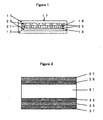
- a representative example is shown in Figure 1 .
- the electrode substrate is a transparent conductive substrate in which a transparent conductive layer (E) is placed on a gas barrier laminated film.
- the gas barrier laminated film has a gas barrier layer (X) and a hardened resin layer (U) on a transparent polymer substrate (S). And, the placing of the transparent conductive layer (E) is performed in such a manner that the transparent electrode (E) is in contact with the hardened resin layer (U).
- a liquid crystal display component having high reliability which is resistant to the deterioration of display quality even when it is allowed to stand in a high-temperature and high-humidity environment for a long time is provided.
- This transparent conductive substrate is also included as one of the objects of the present invention.
- a typical example of such a transparent conductive substrate is shown in Figure 2 .
- a transparent conductive layer (E) 27, a hardened resin layer (U) 29, a transparent polymer substrate (S) 31, a hardened resin layer (B) 33, a gas barrier layer (X) 35 and a hardened resin layer (C) 37 are placed in such a manner that they are in contact with each other in this order.
- Such a transparent conductive substrate has an all-over water absorption coefficient of 2% or less and a total light transmittance of 80% or more, that is, it is low in water absorption and excellent in transparency.
- the conductive substrate therefore can be suitably used naturally as an electrode substrate of a liquid crystal display component in which high reliability and a high gas barrier property are expected, and also in the field of a flat panel display field such as a photosensitive conductor, a surface light emitter, an EL-display or the like.
- a material for a transparent polymer substrate (S) is not specifically limited as far as it is a transparent polymer having excellent transparency and heat resistance.
- a transparent polymer include a polyester resin, a polycarbonate resin, a polyarylate resin, a polysulfone resin such as polysulfone, polyether sulfone or polyarylsulfone, a polyolefin resin, an acetate resin such as cellulose triacetate, a polyacrylate resin, various kinds of thermosetting resins and the like.
- a film or a sheet mainly comprising a polycarbonate resin or a polyarylate resin is more preferable in that it has excellent transparency and heat resistance as mentioned above, and relatively low optical anisotropy.
- the polycarbonate resin is especially suitable when it is formed by a solvent casting method since the obtained film or sheet is excellent in surface smoothness and in optical isotropy.
- polycarbonate resin is a polycarbonate resin whose bisphenol component is a bisphenol expressed by the following formula [1] e.g., 2,2-bis(4-hydroxyphenyl)propane (Bisphenol A).
- R 1 , R 2 , R 3 and R 4 are same as or different from each other, and they are each a hydrogen atom or methyl group
- X is a cycloalkylene group having 5 to 10 carbon atoms, an aralkylene group having 7 to 15 carbon atoms or a haloalkylene group having 1 to 5 carbon atoms.
- Concrete examples of the X when it is a cycloalkylene group, include 1,1-cyclopentylene, 1,1-cyclohexylene, 1,1-(3,3,5-trimethyl)cyclohexylene, norbornane-2,2-diyl and tricyclo[5.2.1.0 2,6 ]decane-8,8'-diyl.
- 1,1-cyclohexylene and 1,1-(3,3,5-trimethyl)cyclohexylene are suitably used in that the raw materials are easily available.
- concrete examples of the X when it is an aralkylene group, include phenylmethylene, diphenylmethylene, 1,1-(1-phenyl)ethylene and 9,9-fluorenylene.
- 2,2-hexafluoropropylene, 2,2-(1,1,3,3-tetrafluoro-1,3-dicyclo)propylene or the like is suitably used as the haloalkylene of the X.
- These compounds may be used singly or plurally.
- 1,1-(3,3,5-trimethyl)cyclohexylene and 9,9-fluorenylene are preferable from the point of view of heat resistance and optical properties required in a liquid crystal display component.
- the above-mentioned bisphenol components may be used in the combination of two or more kinds.
- Such a polycarbonate resin may be a copolymer or may be used in the combination of two or more kinds.
- a polycarbonate resin As such a polycarbonate resin, (i) a homopolymer whose bisphenol component is bisphenol A or (ii) a copolymer whose bisphenol components are bisphenol A and a bisphenol of the above formula [1], wherein the X is 1,1-(3,3,5-trimethyl)cyclohexylene or 9,9-fluorenylene, is further preferable.
- the content of bisphenol A is preferably 10 to 90 mol %.
- the transparent polymer substrate (S) is preferably a film or a sheet having a thickness in the range of 0.01 to 1.0 mm.
- the thickness is less than 0.01 mm, the stiffness is not sufficient, it is easily deformed on panel processing, and it is difficult in handling.
- it is larger than 1.0 mm, it is resistant to deformation, but when such a liquid crystal display component has been assembled, a double-imaging trouble becomes extreme with the result that it deteriorates display quality.
- the preferred thickness is in the range of 0.02 to 0.7 mm.
- the transparent conductive substrate preferably has the following excellent optical isotropy, transparency and non-water-absorption when used as an electrode substrate for a liquid crystal display panel:
- the retardation value is expressed by the product ⁇ n ⁇ d of the difference ⁇ n of the refractive indexes in birefringence at a wave length of 590 nm determined by a known measuring instrument and the thickness d of the film.
- a transparent polymer substrate having a low water absorption coefficient is preferred.
- the substrate absorbs water at a high-temperature high-humidity test, the surface electric resistivity of the base of the transparent conductive layer is lowered, and resultingly the display defect of the panel is apt to occur.
- Such a trouble can be suppressed considerably by the lamination of a gas barrier layer shown below; however, in order to get higher high-temperature high-humidity reliability, it is preferable that the water absorption coefficient of the transparent polymer substrate is 0.7% or less.
- the organic gas barrier layer include a layer formed of a vinyl alcohol polymer such as polyvinyl alcohol or a vinyl alcohol-ethylene copolymer, an acrylonitrile polymer such as polyacrylonitrile, an acrylonitrile-methyl acrylate copolymer or an acrylonitrile-styrene copolymer or a polymer such as polyvinylidene chloride.
- the organic gas barrier layer can be commonly formed by applying a coating composition prepared by dissolving an above-mentioned polymer in an organic solvent on a transparent polymer substrate (S) by a coating method.
- a coating method prepared by dissolving an above-mentioned polymer in an organic solvent on a transparent polymer substrate (S) by a coating method.
- a known method for example, a reverse roll coating method, a micro gravure coating method, a direct gravure coating method, a kiss-roll coating method or a die coating method can be used.
- the viscosity of a coating solution and the film thickness of a gas barrier layer can be controlled by diluting the coating composition with an appropriate organic solvent.
- the thickness of the organic gas barrier layer may be controlled depending on the material to be used so that the water vapor transmission of the whole of the transparent conductive substrate after the removal of the transparent conductive layer from the transparent conductive substrate of the present invention becomes as little as possible in a high-temperature and high-humidity environment; however, usually it is preferably 1 to 50 ⁇ m.
- examples of the inorganic gas barrier layer include a metal oxide mainly of one or more kinds of metals selected from a group consisting of silicon, aluminum, magnesium, zinc, zirconium, titanium, yttrium and tantalum, a metal nitride of silicone, aluminum or boron, and a mixture of these compounds.
- a metal oxide consisting mainly of silicon oxide having the ratio of the number of oxygen atoms to the number of silicon atoms of 1.5 to 2.0 from view points of gas barrier property, transparency, surface smoothness, flexibility, membrane stress, cost and the like.
- the ratio of the number of oxygen atoms to the number of silicone atoms in the silicone oxide is analyzed and determined by X-ray photoelectric spectroscopy, X-ray micro spectroscopy, Auger electron spectroscopy, Rutherford's back scattering method or the like.
- the ratio becomes smaller than 1.5, the transparency is lowered, and so it is preferably 1.5 to 2.0.
- the compounding of magnesium oxide and/or magnesium fluoride in an amount of 5 to 30% by weight based on the total weight in the above-mentioned silicone oxide enables the increase of transparency.
- These inorganic gas barrier layers can be formed by a vapor deposition method which forms a film by depositing a material from a gas phase, for example, such as a sputter technique, a vacuum evaporation method, an ion plating method, a plasma CVD method or the like.
- a sputter technique is preferred in that especially excellent gas barrier property is obtained.
- the film thickness of the inorganic gas barrier layer is preferably in the range of 2 nm to 1 ⁇ m.
- the thickness of the metal oxide layer is less than 2 nm, it is difficult to form a homogeneous layer, and no layer parts are formed with the result that the gas permeability becomes large.
- the thickness is larger than 1 ⁇ m, not only the transparency becomes poor, but also when the transparent conductive substrate is bent, cracks are generated in the gas barrier layer, and the gas permeability is increased.
- the hardened resin layer (B) having a water absorption coefficient larger than that of the transparent polymer substrate (S) is laminated on the surface of the (S) of the opposite side to the surface on which a hardened resin layer (U) is laminated, it is possible to obtain a panel which is further resistant to the deterioration of displaying quality even in the case where it is allowed to stand for a long time in a high-temperature and high-humidity environment.
- a silicon-containing resin such as the (P) or (Q) which will be described later
- a thermosetting resin such as an epoxy resin, a radiation curing resin such as an ultraviolet-curing acrylic resin, a melamine resin, a urethane resin, an alkyd resin, or the like
- an ultraviolet-curing acrylic resin such as acrylic resin
- a melamine resin such as an ultraviolet-curing acrylic resin
- a urethane resin such as an alkyd resin, or the like
- a metal oxide consisting mainly of the above-mentioned silicon oxide is used as the gas barrier layer (X), and a hardened resin layer (B) consisting of a silicon-containing resin and a hardened resin layer (C) consisting of a silicone-containing resin are placed in such a manner that they come into contact with the (X) by sandwiching it.
- a silicon-containing resin a vinyl alcohol-containing polysiloxane resin (P) or an organic polysiloxane resin (Q) is preferable, and it is more preferable that at least one out of hardened resin layers (B) and (C) is the (P).
- the gas transmission of the whole of the substrate can be reduced, and especially, a water vapor transmission can be reduced below 0.1 g/m 2 /day.
- the vinyl alcohol-containing polysiloxane resin (P) can be obtained by using a coating composition containing a vinyl alcohol polymer, an epoxy group-containing silicone compound and an amino group-containing silicon compound.
- the vinyl alcohol polymer means a vinyl alcohol copolymer containing not less than 50 mol % vinyl alcohol or a homopolymer of vinyl alcohol.
- the vinyl alcohol copolymer include a vinyl alcohol-vinyl acetate copolymer, a vinyl alcohol-vinyl butyrate copolymer, an ethylene-vinyl alcohol copolymer or a polyvinyl alcohol having a silyl group in a molecule.
- a vinyl alcohol-containing polysiloxane resin (P) having excellent chemical resistance, water resistance and durability can be obtained.
- the vinyl alcohol polymer is used as a coating composition by dissolving it in a solvent such as water, an alcohol or dimethylimidazoline.
- a solvent such as water, an alcohol or dimethylimidazoline.
- an ethylene-vinyl alcohol copolymer is preferably used as a component of a coating composition by dissolving it in a mixed solvent composed mainly of water and propanol.
- the epoxy group-containing silicon compound is selected from a group consisting of a silicon compound having an epoxy group and an alkoxysilyl group, its (partial) hydrolyzate, its (partial) condensate and their mixture, and it is expressed, for example, by the following formula [II] X-R 11 -Si(R 12 ) n (OR 13 ) 3-n [II]
- R 11 is an alkylene group having 1 to 4 carbon atoms
- R 12 and R 13 are each an alkyl group having 1 to 4 carbon atoms
- X is a glycidoxy group or an epoxycyclohexyl group
- n is 0 or 1.
- An especially preferable epoxy group-containing silicone compound is 3-glycidoxypropyltrimethoxysilane, 2-(3,4-epoxycyclohexy)ethyltrimethoxysilane. These compounds may be used singly or in the combination of two or more kinds.
- the amino group-containing silicon compound is selected from a group consisting of a silicon compound containing an amino group and an alkoxysilyl group, its (partial) hydrolyzate, its (partial) condensate and their mixture, and it is expressed, for example, by the following formula [III].
- Y-HN-R 14 -Si(R 15 ) m (OR 16 ) 3-m [III]
- R 14 is an alkylene group having 1 to 4 carbon atoms
- R 15 and R 16 are each an alkyl group having 1 to 4 carbon atoms
- Y is a hydrogen atom or an aminoalkyl group
- m is 0 or 1.
- an especially preferable amino group-containing silicone compound is 3-aminopropyltrimethoxysilane, 3-aminopropyltriethoxysilane, N-methyl-3-aminopropyltrimethoxysilane, 3-aminopropylmethyldiethoxysilane, N-(2-aminoethyl)-3-aminopropyltrimethoxysilane and N-(2-aminoethyl)-3-aminopropylmethyldimethoxysilane. These compounds may be used singly or in the combination of two or more kinds.
- a (partial) hydrolyzate or a (partial) condensate of an epoxy group-containing silicon compound or an amino group-containing silicon compound is a product of a partial or total hydrolysis of the above-mentioned epoxy group-containing silicon compound or amino group-containing silicon compound, a product of the condensation of a part or the whole of the hydrolyzate with itself, or a product of the condensation of the condensate with the epoxy group-containing silicon compound or the amino group-containing silicon compound which has not been hydrolyzed, i.e. the raw material.
- sol-gel reaction a so-called sol-gel reaction.
- the hydrolysate is obtained, for example, by mixing the raw material with an acidic aqueous solution of an inorganic acid such as hydrochloric acid or an organic acid such as acetic acid, or water.
- the coating solution is preferably diluted with an organic solvent selected from various of an alcohol, an ester, an ether, a ketone, a cellosolve and the like in consideration of storage stability and coating stability.
- the compounding ratio of the epoxy group-containing silicone compound to the amino group-containing silicone compound is expressed by the ratio of the amount Ep of the epoxy-group in terms of molar equivalent to the amount Ap of the amino-group in terms of molar equivalent, it is preferably in the range of 1/6 ⁇ Ep/Ap ⁇ 6/1.
- the compounding ratio is out of the range, adhesiveness, heat resistance, solvent resistance, water resistance and durability become poor.
- the mixing of a mixture of such an epoxy group-containing silicon compound and an amino group-containing silicone compound with a polyvinyl alcohol polymer is carried out in such a manner that the compounding ratio becomes not less than 20% by weight and not more than 95% by weight after hardening.
- the weight of the mixture of the epoxy group-containing silicon compound and the amino group-containing silicon compound after hardening is based on the weight expressed by X-R 11 -Si(R 12 ) n O (3-n)/2 and Y-HN-R 14 -Si(R 15 ) m O (3-m)/2 .
- a gas barrier property is further improved.
- an organic solvent, a catalyst such as acetic acid, a stabilizer and a leveling agent are optionally contained besides the vinyl alcohol polymer, the epoxy group-containing polymer and the amino group-containing polymer.
- concentration of acetic acid in said composition the acetic acid is preferably added in the range of 0.2 to 5 molar equivalents per molar concentration of the amino group and/or imino group in the coating composition.
- the amounts of the organic solvent, stabilizer and leveling agent may be controlled considering workability and/or the film thickness of the hardened resin layer to be obtained.
- the (P) can be obtained by applying the composition on a base material such as the (S) and subjecting it to hardening reaction under heating or the like.
- the heating is carried out usually at a temperature in the range from room temperature to the glass transition temperature of the (S).
- sol-gel reaction of the epoxy group-containing silicon compound and the amino group-containing silicon compound proceeds, and as a result, a part or all of the vinyl alcohol polymer is made to react to obtain a hardened resin layer.
- the thickness of the layer of the polyvinyl alcohol-containing polysiloxane resin (P) can be properly selected from the range roughly of 0.01 to 20 ⁇ m.
- the organic polysiloxane resin (Q) can be obtained by using a coating composition composed of an epoxy group-containing silicon compound and an amino group-containing silicon compound.
- organic polysiloxane resin As the above-mentioned organic polysiloxane resin (Q), an organic silicon compound expressed by the following formula (IV) or the product obtained by subjecting its hydrolysate to so-called sol-gel reaction is preferred.
- R 17 is an organic group having 1 to 10 carbon atoms
- R 18 is a hydrocarbon group having 1 to 6 carbon atoms or a halogenated hydrocarbon group
- X is a hydrolyzing group
- a and b are each 0 or 1.
- Examples of the organic silicon compound expressed by the above-mentioned formula (IV) include tetramethoxysilane, tetraethoxysilane, methyltrimethoxysilane, methyltriethoxysilane, ethyltrimethoxysilane, vinyltrimethoxysilane, vinyltriethoxysilane, 3-methacryloxypropyltrimethoxysilane, 3-mercaptopropyltrimethoxysilane, dimethyldimethoxysilane, 3-glycidoxypropyltrimethoxysilane, 3-glycidoxypropyltriethoxysilane, (3,4-epoxycyclohexyl)ethyltrimethoxysilane, (3,4-epoxycyclohexyl)ethyltriethoxysilane, aminomethyltriethoxysilane, 3-aminopropyltrimethoxysilane, 3-aminopropyltriethoxy
- These compounds can be used singly or in the combination of two or more kinds.
- a mixture composed mainly of an epoxy group-containing silicon compound of the above formula (II) and an amino group-containing silicone compound of the above formula (III).
- the compounding ratio of the epoxy group-containing silicone compound to the amino group-containing silicone compound is expressed by the ratio of the amount Eq of the epoxy-group in terms of molar equivalent to the amount Aq of the amino-group in terms of molar equivalent, it is preferable to use the compounds in the range of 5/95 ⁇ Eq/Aq ⁇ 95/5, from the points of view of chemical resistance and interlayer adhesivity.
- the formation of a gas barrier layer consisting of a metal oxide composed mainly of the above-mentioned silicon oxide on said organic polysiloxane resin layer further improves the gas barrier property.
- the organic polysiloxane resin (Q) can be produced by the same method as for the above-mentioned (P).
- the film thickness of the organic polysiloxane resin (Q) can be properly selected from the range roughly of 0.01 to 20 ⁇ m.
- the hardened resin layer (U) is used by laminating a transparent conductive layer (E) on it.
- the (U) has a surface electric resistivity of 1.0 ⁇ 10 13 ⁇ / ⁇ or more in an environment of 50°C and 30% RH and that of 1.0 ⁇ 10 12 ⁇ / ⁇ or more in an environment of 50°C and 90% RH, and it can provide a liquid crystal display component which is free from a display defect in a liquid crystal panel for a long time, and has high stability and reliability.
- said hardened resin layer (U) it is preferable to suppress polar groups, water absorption and ionic impurities as low as possible.
- the more the content of the polar groups such as a hydroxyl group, an amino group, an amide group or a carbonyl group the higher the absorption and the more the contamination of ionic impurities are, the more extreme the decreasing of surface electric resistivity is.
- the polar groups exist in some degree, the interlayer close adhesion of transparent conductive substrates can not be secured.
- the water absorption varies depending on the structure of a hardened resin layer and the layer forming conditions, and a highly cross-linked layer is preferable.
- thermosetting resin which can obtain sufficient objective properties with a short heat treatment is more preferred.
- the contamination of ionic impurities or the like must be suppressed as low as possible, of course, in the purification of the raw material of the hardened resin layer (U) but also in the manufacturing process of the transparent conductive substrate.
- Such a hardened resin layer (U) is required to have chemical resistance, transparency and excellent interlayer adhesivity.
- the hardened resin layer (11) includes an acrylic resin which contains the units of the following formula (V) and, optionally, formula (VI)
- Such a resin may be compounded with a known hydrolysate of an alkoxysilane or silane coupling agent in order to impart further adhesivity and solvent resistance.
- a known hydrolysate of an alkoxysilane or silane coupling agent in order to impart further adhesivity and solvent resistance.
- the above-mentioned radiation curing resin is usually compounded with an adequate amount of a known optical reaction initiator.
- the film thickness of the above-mentioned resin layer (U) can be adequately selected from the range roughly of 0.01 to 20 ⁇ m, preferably 0.03 to 10 ⁇ m.
- the above-mentioned hardened resin layer (U) can be manufactured by a conventional method comprising the application of a composition prepared by mixing a hardening resin in an organic solvent on a base material followed by the heating or ultraviolet irradiation to harden the resin.
- the layer (U) can be formed by the above-mentioned method.
- the present invention gives a transparent conductive substrate having the above-mentioned excellent properties and excellent gas barrier property by placing the transparent conductive layer (E) in such a manner that it is in contact with the hardened resin layer (U) of a gas barrier laminated film comprising the above-mentioned transparent polymer substrate (S), gas barrier layer (X) and hardened resin layer (U). That is, the laminated film has a high value of surface electric resistivity in the layer (U) even in a high-temperature and high-humidity environment, and at the same time the laminated film is excellent in a gas barrier property and has a water absorption coefficient of 2% or less.
- the laminated film has a water vapor transmission of 1 g/m 2 /day or less, preferably 0.1 g/m 2 /day or less in an environment of 40°C and 90% RH, and further, the surface of the (U) exhibits a high insulation resistance in a high-temperature and high-humidity environment.
- the transparent conductive layer (E) a known metal layer, metal oxide layer or the like can be used; however, the metal oxide layer is especially preferable from the points of view of transparency, conductivity and mechanical properties.
- the transparent conductive layer (E) include metal oxide layers of indium oxide, cadmium oxide and tin oxide to which tin, tellurium, cadmium, molybdenum, tungsten, fluorine, zinc, germanium or the like is added as an impurity, and zinc oxide, titanium oxide and the like to which aluminum is added as an impurity.
- a thin film of an indium oxide containing 2 to 15% by weight tin oxide as an impurity or a thin film of an indium oxide containing 2 to 15% by weight zinc oxide as an impurity is preferable since it is excellent in transparency, and conductivity.
- the film thickness of the above-mentioned transparent conductive layer (E) is determined depending the objective surface electric resistivity, but it is 1 nm to 1 ⁇ m, preferably 10 nm to 500 nm.
- the transparent conductive substrate prepared by laminating layers in the following order is preferable, for example,
- various kinds of chemical treatments, or physical treatments such as corona treatment, plasma treatment or UV-irradiation on the lamination or the like of undercoat layers for intensifying each interlayer adhesion can be performed as long as the effect of the present invention is not lowered.
- the adhesivity preferably further increases.
- a urethane resin is preferable for the hardened resin layer (A).
- the transparent conductive substrate of the present invention When the transparent conductive substrate of the present invention is handled in a film roll state, it is efficient to place a slipperiness-imparting layer on the opposite side to the side where a transparent conductive layer is laminated or to subject that side to a knurling treatment.
- a color filter layer can be formed optionally on the transparent conductive layer of the present invention, for example, with the object of imparting a color display function to the liquid crystal display component produced by using the substrate.
- the color filter can be formed by a known technology such as a dyeing method, a pigment dispersion method, an electrodeposition technique or a printing method. It is preferable that the color filter layer is formed at an interlayer space other than that between the transparent conductive layer (E) and the hardened resin layer (U) of a transparent conductive substrate or on the outermost side which is opposite to the side where the transparent conductive layer (E) is laminated since this makes easy to secure the motional reliability of the liquid crystal panel to be formed.
- the transparent conductive substrate of the present invention has excellent transparency, optical isotropy, chemical resistance, interlayer adhesivity and gas barrier properties; and it is extremely useful as a transparent conductive substrate which can give a liquid crystal panel resistant to the occurrence of the deterioration of display quality even after long standing in a high-temperature and high-humidity environment.
- Water vapor barrier property A water vapor transmission in an atmosphere of 40°C and 90% RH was measured by using permatran W1A manufactured by Mocon Company.
- Water absorption coefficients of a transparent polymer substrate (S), the whole of a transparent conductive substrate and a hardened resin layer (B) were each measured according to ASTM D570.
- the measuring sample was prepared by mixing the above-obtained sample with KBr at a ratio of 0.3 part to 100 pats by weight.
- an FT-IR manufactured by Perkin-Elmer Corporation was used.
- Optical isotropy The retardation value against the light having a wave length of 590 nm was measured by using a multi-wavelength refractometer M-150 manufactured by Nippon Bunko.
- Interlayer adhesivity The interlayer adhesive strengths of the layers constituting a transparent conductive substrate were each evaluated according to ASTM D2196-68.
- a liquid crystal display component shown in Figure 1 was prepared and the reliability was evaluated on the component.
- the liquid crystal display component has the following structure: an upper side laminated film having a gas barrier property (hereafter, a gas barrier laminated film is referred to as a laminated film) 11 and the lower laminated film 13 are placed at positions facing each other, and the edge parts of the laminated films 11 and 13 are sealed with a sealing material 15 and pieces of a gapping material 21 are dispersed to form a liquid crystal cell 17; a liquid crystal material 19 is enclosed in the liquid crystal cell 17; polarizing plates are placed in such a manner that the liquid crystal cell 17 is held between them to constitute an STN-type liquid crystal display component; on the upper laminated film 11, a transparent conductive layer 23 which has been subjected to a patterning treatment is placed to constitute a transparent conductive substrate of the present invention; on the lower laminated film 13, a transparent conductive layer 23 which has not been subjected to a patterning treatment is placed to constitute a transparent
- a display electrode for 160 ⁇ 100 dots was formed on the transparent conductive layer by photolithography. Subsequently, on the surface of the electrode, an alignment layer 1000 ⁇ thick was formed, and the alignment layer was subjected to a rubbing treatment so that the twist angle becomes 220°. Then, plastic beads of 6.5 ⁇ m in diameter as a gapping agent were dispersed on the inside surface of the electrode surface in such a manner that the dispersion density became 150 piece/mm 2 , and two sheets of the transparent conductive substrates were stuck together with an epoxy adhesive in such a manner that the electrode surfaces were placed inwardly to form a cell.
- a nematic liquid crystal containing chiral nematic liquid crystal was infused into the cell from an inlet, and the inlet was sealed after the cell gap was leveled by a pressuring method.
- polarizing plates were laminated on both the sides of the cell to obtain a liquid crystal panel.
- liquid crystal panel was allowed to stand in an environment of 50°C and 90% RH for 250 hr, and the decrease of impedance of the liquid cell was examined.
- a polycarbonate (BisA-PC) having the bisphenol component consisting only of BisA and having an average molecular weight of 37,000 and Tg of 155°C was dissolved in methylene chloride in such a manner as to become 20% by weight. This solution was cast on a polyester film 175 ⁇ m thick by a die coating method. Subsequently, the coated film was dried in a drying furnace until the remaining solvent concentration became 13% by weight, and the polycarbonate film was peeled from the polyester film. The obtained polycarbonate film was dried in a drying furnace of 120°C until the remaining solvent concentration in the film became 0.08% by weight under holding the balance between longitudinal and lateral tensions.
- Thus-obtained transparent polymer substrate (S) has a thickness of 100 ⁇ m and a light transmittance of 91% at a wave-length of 550 nm.
- a coating composition for forming a polyvinyl alcohol-containing polysiloxane resin layer (P) was prepared as follows.
- the component (P1) EVOH in an amount of 100 parts was dissolved under heating in a mixed solvent of 720 parts of water and 1080 parts of n-propanol to obtain a homogeneous solution.
- a leveling agent SH30PA manufacture by Toray Dow Corning Co., Ltd.
- acetic acid 39 parts of acetic acid
- 211 parts of the component (P2) ECHETMOS was added, and the mixture was stirred for 10 min.
- 77 parts of the component (P3) APTMOS was added to the obtained solution, and the mixture was stirred for 3 hr to obtain the objective coating composition.
- This coating composition was applied on one side of the above-mentioned transparent polymer substrate (S), then the coated substrate was subjected to a thermal treatment at 130°C for 3 min to form a layer (P) of 0.05 ⁇ m in thickness.
- a gas barrier layer (X) consisting of an SiO 2 layer of 250 ⁇ in thickness was laminated on a layer (B) by a DC magnetron sputtering method.
- a transparent conductive layer (E) consisting of an ITO layer of 130 nm in thickness was formed on the surface of the opposite side to the (X)-laminated face of the film by a DC magnetron sputtering method, and as the result, a transparent conductive substrate was obtained.
- the evaluation results of the obtained transparent conductive substrate were good as shown in Table 1.
- a liquid crystal display component prepared by using the transparent conductive substrate of the present invention showed completely no visual observation defect such as orientation deterioration in a high-temperature preservation test at 80°C for 1000 hr, and the increase of power consumption was within 20% of the initial value; and high reliability was exhibited.
- a coating composition was obtained by mixing 10 parts of DCPA, 10 parts of EA, 10 parts of UA, 30 parts of 1-meihoxy-2-propanol and 2 parts of 1-hydroxycyclohexyl phenyl ketone as an initiator, by weight. By applying the obtained composition and heating at 60 °C for 1 min followed by irradiation with a high-pressure mercury lamp, the hardened resin layer (U) was formed.
- a coating composition was obtained by mixing 20 parts of DCPA, 10 parts of UA, 30 parts of 1-methoxy-2-propanol and 2 parts of 1-hydroxycyclohexyl phenyl ketone as an initiator, by weight. By applying the obtained composition and heating at 60 °C for 1 min followed by irradiation with a high-pressure mercury lamp, the hardened resin layer (U) was formed.
- the liquid crystal display component of the present invention is resistant to the deterioration of the display quality for a long time and has an extremely high reliability since a transparent conductive substrate containing a hardened resin layer, which is placed in the lower layer of a transparent conductive layer and has an excellent insulation characteristic in a high-temperature and high-humidity environment, is used as an electrode substrate.
- the transparent conductive substrate is excellent also in a gas barrier property, and it can be used suitably as an electrode substrate in the field of a flat panel display such as a photosensitive conductor, a surface light emitter, an EL-display or the like.
Landscapes
- Physics & Mathematics (AREA)
- Nonlinear Science (AREA)
- Mathematical Physics (AREA)
- Chemical & Material Sciences (AREA)
- Crystallography & Structural Chemistry (AREA)
- General Physics & Mathematics (AREA)
- Optics & Photonics (AREA)
- Liquid Crystal (AREA)
- Laminated Bodies (AREA)
Claims (16)
- Transparentes leitfähiges Substrat, umfassend eine Gasbarrierelaminatfolie, welche umfasst: ein transparentes polymeres Substrat (S), eine Gasbarrierelage (X), bestehend aus einem Metalloxid, einem Metallnitrid oder deren Mischung, und eine gehärtete Harzschicht (U), und eine transparente leitfähige Lage (E), welche in Kontakt mit der gehärteten Harzlage (U) der Laminatfolie platziert ist, dadurch gekennzeichnet, dass(i) der Wasserabsorptionskoeffizient 2 % oder weniger beträgt,(ii) die Gesamtlichtdurchlässigkeit 80 % oder mehr beträgt,(iii) die Dicke des transparenten polymeren Substrats (S) 0,01 bis 1,0 mm beträgt,(iv) die Retardation des transparenten polymeren Substrats (S) 20 nm oder weniger beträgt,(v) die Dicke der Gasbarrierelage (X) 5 bis 200 nm beträgt,(vi) die Dicke der transparenten leitfähigen Lage (E) 1 nm bis 1 µm beträgt,(vii) die gehärtete Harzlage (U) einen spezifischen elektrischen Oberflächenwiderstand von 1,0 x 10¹³ Ω/□ oder mehr in einer Umgebung von 50 °C und 30 % rF und von 1,0 x 10¹² Ω/□ oder mehr in einer Umgebung von 50 °C und 90 % rF aufweist, wobei die gehärtete Harzlage (U) ein Acrylharz umfasst, welches die Einheiten der folgenden Formel (V) enthält:

- Transparentes leitfähiges Substrat nach Anspruch 1, wobei die gehärtete Harzlage (U) ferner ein Acrylharz umfasst, welches die Einheiten der folgenden Formel (VI) enthält
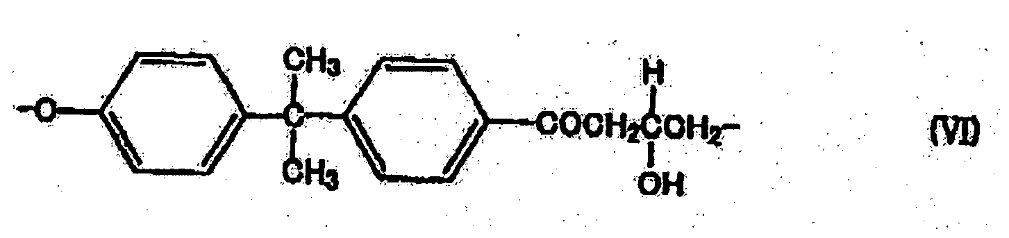
- Transparentes leitfähiges Substrat nach Anspruch 1, wobei die Laminatfolie eine Wasserdampfdurchlässigkeit von 1 g/m2/Tag oder weniger in einer Umgebung von 40 °C und 90 % rF aufweist.
- Transparentes leitfähiges Substrat nach Anspruch 1, wobei eine gehärtete Harzlage (B) auf der Seite platziert ist, welche der Seite, wo die gehärtete Harzlage (U) des transparenten polymeren Substrats (S) platziert ist, gegenüberliegt, derart, dass die Lage (B) mit dem Substrat (S) in Kontakt ist, und wobei der Wasserabsorptionskoeffizient der Lage (B) größer ist als derjenige des Substrats (S).
- Transparentes leitfähiges Substrat nach Anspruch 4, wobei der Wasserabsorptionskoeffizient des transparenten polymeren Substrats (S) 1 % oder weniger beträgt.
- Transparentes leitfähiges Substrat nach Anspruch 4, wobei die gehärtete Harzlage (B) ein Vinylalkohol-haltiges Polysiloxanharz (P), erhältlich aus einer Beschichtungszusammensetzung, die ein Vinylalkohol-Polymer, eine Epoxygruppen-haltige Siliciumverbindung und eine Aminogruppen-haltige Siliciumverbindung enthält, oder ein organisches Polysiloxanharz (Q), erhältlich aus einer Beschichtungszusammensetzung, die eine Epoxygruppen-haltige Siliciumverbindung und eine Aminogruppen-haltige Siliciumverbindung enthält, umfasst.
- Transparentes leitfähiges Substrat nach Anspruch 1, wobei die Laminatfolie ferner eine gehärtete Harzlage (B) und eine gehärtete Harzlage (C) umfasst und wobei die Gasbarrierelage (X) in Kontakt mit der gehärteten Harzlage (B) und der gehärteten Harzlage (C) platziert ist.
- Transparentes leitfähiges Substrat nach Anspruch 7, wobei die gehärtete Harzlage (B) ein Vinylalkohol-haltiges Polysiloxanharz (P), erhältlich aus einer Beschichtungszusammensetzung, die ein Vinylalkohol-Polymer, eine Epoxygruppen-haltige Siliciumverbindung und eine Aminogruppen-haltige Siliciumverbindung enthält, oder ein organisches Polysiloxanharz (Q), erhältlich aus einer Beschichtungszusammensetzung, die eine Epoxygruppen-haltige Siliciumverbindung und eine Aminogruppen-haltige Siliciumverbindung enthält, umfasst und wobei die gehärtete Harzlage (C) das oben erwähnte Harz (P) oder (Q) umfasst.
- Transparentes leitfähiges Substrat nach Anspruch 8, wobei die Dicke der Gasbarrierelage (X) im Bereich von 5 bis 50 nm liegt.
- Transparentes leitfähiges Substrat nach Anspruch 1, wobei das Metalloxid hauptsächlich aus einem Siliciumoxid besteht, mit einem Verhältnis der Zahl von Sauerstoffatomen zu derjenigen der Siliciumatome von 1,5 bis 2,0.
- Transparentes leitfähiges Substrat nach Anspruch 1, wobei das transparente polymere Substrat (S) hauptsächlich aus Polycarbonat oder Polyacrylat besteht und eine Gesamtlichtdurchlässigkeit von 80 % oder mehr und eine Retardation von 20 nm oder weniger aufweist.
- Transparentes leitfähiges Substrat nach Anspruch 1, ferner umfassend eine gehärtete Harzlage (A), wobei die gehärtete Harzlage (A) zwischen der gehärteten Harzlage (U) und dem transparenten polymeren Substrats (S) platziert ist, derart, dass die Lage (A) in Kontakt mit der Lage (U) und dem Substrat (S) ist.
- Transparentes leitfähiges Substrat nach Anspruch 1, ferner umfassend eine gehärtete Harzlage (A), eine gehärtete Harzlage (B) und eine gehärtete Harzlage (C), wobei die gehärtete Harzlage (U), die gehärtete Harzlage (A), das transparente polymere Substrat (S), die gehärtete Harzlage (B), die ein Metalloxid, ein Metallnitrid oder deren Mischung umfassende Gasbarrierelage (X) und die gehärtete Harzlage (C) in dieser Reihenfolge in Kontakt miteinander sind und wobei:(viii) die Laminatfolie eine Wasserdampfdurchlässigkeit von 0,1 g/m2/Tag oder weniger in einer Umgebung von 40 °C und 90 % rF aufweist.
- Transparentes leitfähiges Substrat nach Anspruch 13, wobei die gehärtete Harzlage (U) ein Vinylalkohol-haltiges Polysiloxanharz (P), erhältlich aus einer Beschichtungszusammensetzung, die ein strahlungshärtendes Harz oder ein Vinylalkohol-Polymer, eine Epoxygruppen-haltige Siliciumverbindung und eine Aminogruppen-haltige Siliciumverbindung enthält, oder ein organisches Polysiloxanharz (Q), erhältlich aus einer Beschichtungszusammensetzung, die eine Epoxygruppen-haltige Siliciumverbindung und eine Aminogruppen-haltige Siliciumverbindung enthält, umfasst, wobei die gehärtete Harzlage (B) das oben erwähnte Harz (P) oder (Q) umfasst und wobei die gehärtete Harzlage (C) das oben erwähnte Harz (P) oder (Q) umfasst.
- Transparentes leitfähiges Substrat nach Anspruch 14, wobei die Gasbarrierelage (X) ein Metalloxid umfasst, welches hauptsächlich aus Siliciumoxid besteht, und wobei das Silicium-haltige Harz die folgenden Formeln (1), (2) und (3) erfüllt:


worin (a) die einer in der Nähe von 3500 cm-1 existierenden O-H-Streckschwingung zugeordnete Extinktion, (b) die einer in der Nähe von 3000 cm-1 existierenden C-H-Streckschwingung zugeordnete Extinktion, (c) die einer in der Nähe von 1600 cm-1 existierenden -NH2-De-formationsschwingung in der Ebene zugeordnete Extinktion und (d) die auf eine in der Nähe von 1100 cm-1 existierende Si-O-Bindung zurückzuführende Extinktion im Infrarotabsorptionsspektrum sind. - Flüssgkristallanzeigekomponente, umfassend ein Paar von Elektrodensubstraten wie in einem der Ansprüche 1 bis 15 definiert und zwischen denen eine Flüssigkristalllage angeordnet ist.
Priority Applications (1)
| Application Number | Priority Date | Filing Date | Title |
|---|---|---|---|
| EP20080075083 EP1921491A1 (de) | 1998-11-30 | 1999-11-26 | Flüssigkristallanzeige und dafür geeignetes durchsichtiges, leitfähiges Substrat |
Applications Claiming Priority (5)
| Application Number | Priority Date | Filing Date | Title |
|---|---|---|---|
| JP33967798 | 1998-11-30 | ||
| JP33967798 | 1998-11-30 | ||
| JP22623799 | 1999-08-10 | ||
| JP11226237A JP2001052530A (ja) | 1999-08-10 | 1999-08-10 | 透明導電性基板 |
| PCT/JP1999/006613 WO2000033127A1 (en) | 1998-11-30 | 1999-11-26 | Liquid crystal device and transparent conductive substrate preferable to the same |
Related Child Applications (1)
| Application Number | Title | Priority Date | Filing Date |
|---|---|---|---|
| EP20080075083 Division EP1921491A1 (de) | 1998-11-30 | 1999-11-26 | Flüssigkristallanzeige und dafür geeignetes durchsichtiges, leitfähiges Substrat |
Publications (3)
| Publication Number | Publication Date |
|---|---|
| EP1063560A1 EP1063560A1 (de) | 2000-12-27 |
| EP1063560A4 EP1063560A4 (de) | 2003-06-04 |
| EP1063560B1 true EP1063560B1 (de) | 2009-07-15 |
Family
ID=26527076
Family Applications (2)
| Application Number | Title | Priority Date | Filing Date |
|---|---|---|---|
| EP99973131A Expired - Lifetime EP1063560B1 (de) | 1998-11-30 | 1999-11-26 | Fluessigkristallanzeige und dafuer bevorzugtes transparantes, leitfaehiges substrat |
| EP20080075083 Withdrawn EP1921491A1 (de) | 1998-11-30 | 1999-11-26 | Flüssigkristallanzeige und dafür geeignetes durchsichtiges, leitfähiges Substrat |
Family Applications After (1)
| Application Number | Title | Priority Date | Filing Date |
|---|---|---|---|
| EP20080075083 Withdrawn EP1921491A1 (de) | 1998-11-30 | 1999-11-26 | Flüssigkristallanzeige und dafür geeignetes durchsichtiges, leitfähiges Substrat |
Country Status (7)
| Country | Link |
|---|---|
| US (2) | US6369871B1 (de) |
| EP (2) | EP1063560B1 (de) |
| KR (1) | KR100542062B1 (de) |
| CA (1) | CA2319382C (de) |
| DE (1) | DE69941114D1 (de) |
| TW (1) | TW484029B (de) |
| WO (1) | WO2000033127A1 (de) |
Families Citing this family (32)
| Publication number | Priority date | Publication date | Assignee | Title |
|---|---|---|---|---|
| CA2352567A1 (en) * | 2001-07-06 | 2003-01-06 | Mohamed Latreche | Translucent material displaying ultra-low transport of gases and vapors, and method for its production |
| JP3866591B2 (ja) * | 2001-10-29 | 2007-01-10 | 富士通株式会社 | 電極間接続構造体の形成方法および電極間接続構造体 |
| US20030207093A1 (en) * | 2001-12-03 | 2003-11-06 | Toshio Tsuji | Transparent conductive layer forming method, transparent conductive layer formed by the method, and material comprising the layer |
| US6866949B2 (en) * | 2002-03-08 | 2005-03-15 | Dai Nippon Printing Co., Ltd. | Substrate film, gas barrier film, and display using the same |
| JP2004127719A (ja) * | 2002-10-02 | 2004-04-22 | Nippon Hoso Kyokai <Nhk> | 透明導電性フィルム及び表示装置 |
| EP1574882B1 (de) * | 2002-12-20 | 2013-01-23 | Teijin Limited | Transparentes leitfähiges laminat, berührungstafel und flüssigkristallanzeigeeinheit mit berührungstafel |
| JP4654911B2 (ja) * | 2003-05-16 | 2011-03-23 | 凸版印刷株式会社 | 透明ガスバリア積層フィルム、これを用いたエレクトロルミネッセンス発光素子、エレクトロルミネッセンス表示装置、及び電気泳動式表示パネル |
| US20060257760A1 (en) * | 2003-08-11 | 2006-11-16 | Kenichi Mori | Near-infrared absorbing film, and process for production the same, near-infrared absorbing film roll, process for producing the same and near-infrared absorbing filter |
| JPWO2005100014A1 (ja) * | 2004-04-15 | 2008-03-06 | 帝人株式会社 | 透明ガスバリア性積層フィルム |
| JP4365792B2 (ja) * | 2005-01-19 | 2009-11-18 | 株式会社フューチャービジョン | 液晶表示装置 |
| JP4652122B2 (ja) * | 2005-05-18 | 2011-03-16 | 株式会社日立製作所 | 投射型映像表示装置、それに用いる光学部材及び光学ユニット |
| US20060286370A1 (en) * | 2005-06-21 | 2006-12-21 | Tang-Chia Chiu | Nano protective film structure |
| US20070058114A1 (en) * | 2005-09-12 | 2007-03-15 | Asahi Glass Company, Limited | Light control device |
| KR100789617B1 (ko) * | 2005-09-13 | 2007-12-27 | 주식회사 엘지화학 | 네가티브 c 타입의 보상 필름 및 이의 제조 방법 |
| US20070096631A1 (en) * | 2005-11-01 | 2007-05-03 | Un-Cheol Sung | Flat panel display and fabricating method thereof |
| KR101386563B1 (ko) * | 2006-06-30 | 2014-04-21 | 엘지디스플레이 주식회사 | 플렉서블 표시장치 제조방법 |
| JP5520528B2 (ja) * | 2008-07-10 | 2014-06-11 | 東レ・ダウコーニング株式会社 | ガスバリアー性硬化オルガノポリシロキサン樹脂フィルム及びその製造方法 |
| CN102216074B (zh) * | 2008-11-19 | 2015-06-24 | Lg化学株式会社 | 层压的塑料基板及其制备方法 |
| JP5343058B2 (ja) * | 2010-10-15 | 2013-11-13 | リンテック株式会社 | 透明導電性フィルム、その製造方法、電子デバイス用部材及び電子デバイス |
| KR101308480B1 (ko) * | 2011-06-14 | 2013-09-16 | 엘지디스플레이 주식회사 | 플라스틱 유기 전계 발광 표시 장치 및 그 제조 방법 |
| US9580625B2 (en) * | 2011-08-03 | 2017-02-28 | Lintec Corporation | Gas barrier adhesive sheet, method for producing same, electronic member, and optical member |
| KR102168722B1 (ko) * | 2011-11-04 | 2020-10-22 | 린텍 가부시키가이샤 | 가스 배리어 필름 및 그 제조 방법, 가스 배리어 필름 적층체, 전자 디바이스용 부재, 그리고 전자 디바이스 |
| KR20130101331A (ko) * | 2012-03-05 | 2013-09-13 | 삼성디스플레이 주식회사 | 액티브 리타더 및 이를 갖는 표시 장치의 제조 방법 |
| JPWO2014084352A1 (ja) * | 2012-11-30 | 2017-01-05 | リンテック株式会社 | 接着剤組成物、接着シート、電子デバイス及びその製造方法 |
| JP5923441B2 (ja) * | 2012-12-21 | 2016-05-24 | 株式会社ジャパンディスプレイ | 表示装置及びヘッドアップディスプレイ |
| DE102014202718A1 (de) * | 2014-02-14 | 2015-08-20 | Evonik Degussa Gmbh | Beschichtungszusammensetzung, Verfahren zu ihrer Herstellung und ihre Verwendung |
| JP2017105013A (ja) * | 2015-12-08 | 2017-06-15 | 株式会社リコー | ガスバリア性積層体、半導体装置、表示素子、表示装置、システム |
| TWI598669B (zh) * | 2016-06-20 | 2017-09-11 | 明基材料股份有限公司 | 液晶裝置 |
| PL233211B1 (pl) * | 2017-01-25 | 2019-09-30 | Saule Spolka Z Ograniczona Odpowiedzialnoscia | Folia optoelektroniczna oraz sposób wytwarzania folii optoelektronicznej |
| WO2019208261A1 (ja) * | 2018-04-27 | 2019-10-31 | 日東電工株式会社 | 調光フィルムおよび液晶表示装置 |
| KR102382553B1 (ko) * | 2018-08-14 | 2022-04-04 | 주식회사 엘지화학 | 광학 디바이스 |
| KR102736669B1 (ko) * | 2021-06-23 | 2024-12-03 | (주)이녹스첨단소재 | 디스플레이용 접착 필름 |
Family Cites Families (14)
| Publication number | Priority date | Publication date | Assignee | Title |
|---|---|---|---|---|
| US5208299A (en) * | 1992-04-10 | 1993-05-04 | The Dow Chemical Company | Nonlinear optical arylhydrazones and nonlinear optical polymers thereof |
| JPH0625399A (ja) * | 1992-07-07 | 1994-02-01 | Teijin Chem Ltd | 光カード用基材 |
| JP3726241B2 (ja) * | 1993-03-29 | 2005-12-14 | 東レ株式会社 | プラスチック光学物品とその製造方法 |
| US5478518A (en) | 1993-10-04 | 1995-12-26 | Teijin Limited | Polycarbonate film for optical purposes and a production process thereof |
| JP3017912B2 (ja) * | 1993-12-13 | 2000-03-13 | シャープ株式会社 | 液晶表示装置用電極基板及び液晶表示装置 |
| JPH08166581A (ja) * | 1994-12-14 | 1996-06-25 | Kanegafuchi Chem Ind Co Ltd | 耐熱性光学プラスチック積層シート及びその製造方法 |
| JPH08211376A (ja) * | 1995-02-02 | 1996-08-20 | Teijin Ltd | 透明積層フィルム |
| DE69729022T2 (de) * | 1996-03-25 | 2005-06-09 | Teijin Ltd. | Beschichtungszusammensetzung, transparentes Elektrodensubstrat mit einer solchen Beschichtung und Flüssigkristallanzeigeelement mit einem solchen Substrat |
| JP3589331B2 (ja) * | 1996-05-28 | 2004-11-17 | 東洋紡績株式会社 | 電極基板 |
| EP0943640A4 (de) * | 1997-10-03 | 2002-02-27 | Unitika Ltd | Hochwärmbeständige, hochreine polyarylate und daraus hergestellte filme |
| EP0914926B1 (de) * | 1997-11-07 | 2002-09-11 | Rohm And Haas Company | Verfahren und Vorrichtung zum Formen einer Kunststoffplatte |
| US6270863B1 (en) * | 1997-11-07 | 2001-08-07 | Rohm And Haas Company | Process and apparatus for forming plastic sheet |
| US6322860B1 (en) * | 1998-11-02 | 2001-11-27 | Rohm And Haas Company | Plastic substrates for electronic display applications |
| US6638582B1 (en) * | 1999-07-29 | 2003-10-28 | Teijin Limited | Phase difference film, phase difference film composite and liquid crystal display device using the same |
-
1999
- 1999-11-26 CA CA 2319382 patent/CA2319382C/en not_active Expired - Fee Related
- 1999-11-26 US US09/601,253 patent/US6369871B1/en not_active Expired - Fee Related
- 1999-11-26 WO PCT/JP1999/006613 patent/WO2000033127A1/ja not_active Ceased
- 1999-11-26 DE DE69941114T patent/DE69941114D1/de not_active Expired - Lifetime
- 1999-11-26 EP EP99973131A patent/EP1063560B1/de not_active Expired - Lifetime
- 1999-11-26 EP EP20080075083 patent/EP1921491A1/de not_active Withdrawn
- 1999-11-26 KR KR1020007008271A patent/KR100542062B1/ko not_active Expired - Fee Related
- 1999-11-26 TW TW88120736A patent/TW484029B/zh not_active IP Right Cessation
-
2002
- 2002-02-06 US US10/066,594 patent/US6734946B2/en not_active Expired - Fee Related
Also Published As
| Publication number | Publication date |
|---|---|
| WO2000033127A1 (en) | 2000-06-08 |
| DE69941114D1 (de) | 2009-08-27 |
| EP1063560A1 (de) | 2000-12-27 |
| CA2319382C (en) | 2010-08-10 |
| CA2319382A1 (en) | 2000-06-08 |
| EP1063560A4 (de) | 2003-06-04 |
| TW484029B (en) | 2002-04-21 |
| KR20010034462A (ko) | 2001-04-25 |
| US6369871B1 (en) | 2002-04-09 |
| KR100542062B1 (ko) | 2006-01-12 |
| EP1921491A1 (de) | 2008-05-14 |
| US6734946B2 (en) | 2004-05-11 |
| US20020140890A1 (en) | 2002-10-03 |
Similar Documents
| Publication | Publication Date | Title |
|---|---|---|
| US6734946B2 (en) | Liquid crystal display component and transparent conductive substrate suitable for the same | |
| JP2000227603A (ja) | 液晶表示素子及びそれに好適な透明導電性基板 | |
| EP0798590B1 (de) | Beschichtungszusammensetzung, transparentes Elektrodensubstrat mit einer solchen Beschichtung und Flüssigkristallanzeigeelement mit einem solchen Substrat | |
| US20110232726A1 (en) | Barrier laminate, method of manufacturing the laminate, gas barrier film and device | |
| JP3370205B2 (ja) | 透明導電基板 | |
| US20110236674A1 (en) | Barrier laminate, method of manufacturing the laminate, gas barrier film and device | |
| EP2138532B1 (de) | Laminat mit Barrierewirkung, Gassperrfolie und Vorrichtung | |
| JP2004330507A (ja) | ディスプレイ用に適したガスバリア性高分子積層フィルム | |
| JP3655704B2 (ja) | 透明導電性積層体 | |
| JPH10146929A (ja) | 透明ガスバリアー性積層フィルム | |
| JP4429467B2 (ja) | 透明導電性フィルム | |
| JP2004330623A (ja) | ディスプレイ用に適したガスバリア性高分子積層フィルム | |
| JP2001052530A (ja) | 透明導電性基板 | |
| JPH0929885A (ja) | 透明導電性フィルム | |
| HK1118101A (en) | Liquid crystal device and transparent conductive substrate suitable for the same | |
| JP2002052636A (ja) | 透明導電性基板 | |
| JP3667933B2 (ja) | 透明電極基板及びそれを用いた液晶表示素子 | |
| JPH11174424A (ja) | 液晶表示パネル用基板 | |
| JP4233180B2 (ja) | 透明導電性高分子基板 | |
| JP2004099754A (ja) | 光学用フィルム | |
| KR100475418B1 (ko) | 투명전극기판을갖는액정표시소자및투명전극기판 | |
| JP2004103292A (ja) | 複層フィルム | |
| JPH09254303A (ja) | 透明導電フィルム | |
| JPH1166969A (ja) | 透明導電フィルム | |
| JP3794731B2 (ja) | 偏光機能を有する電極フィルム |
Legal Events
| Date | Code | Title | Description |
|---|---|---|---|
| PUAI | Public reference made under article 153(3) epc to a published international application that has entered the european phase |
Free format text: ORIGINAL CODE: 0009012 |
|
| 17P | Request for examination filed |
Effective date: 20000815 |
|
| AK | Designated contracting states |
Kind code of ref document: A1 Designated state(s): AT BE CH CY DE DK ES FI FR GB GR IE IT LI LU MC NL PT SE |
|
| A4 | Supplementary search report drawn up and despatched |
Effective date: 20030417 |
|
| RBV | Designated contracting states (corrected) |
Designated state(s): BE DE GB NL SE |
|
| 17Q | First examination report despatched |
Effective date: 20050623 |
|
| GRAP | Despatch of communication of intention to grant a patent |
Free format text: ORIGINAL CODE: EPIDOSNIGR1 |
|
| GRAS | Grant fee paid |
Free format text: ORIGINAL CODE: EPIDOSNIGR3 |
|
| GRAA | (expected) grant |
Free format text: ORIGINAL CODE: 0009210 |
|
| AK | Designated contracting states |
Kind code of ref document: B1 Designated state(s): BE DE GB NL SE |
|
| REG | Reference to a national code |
Ref country code: GB Ref legal event code: FG4D |
|
| REF | Corresponds to: |
Ref document number: 69941114 Country of ref document: DE Date of ref document: 20090827 Kind code of ref document: P |
|
| PG25 | Lapsed in a contracting state [announced via postgrant information from national office to epo] |
Ref country code: SE Free format text: LAPSE BECAUSE OF FAILURE TO SUBMIT A TRANSLATION OF THE DESCRIPTION OR TO PAY THE FEE WITHIN THE PRESCRIBED TIME-LIMIT Effective date: 20090715 |
|
| PLBE | No opposition filed within time limit |
Free format text: ORIGINAL CODE: 0009261 |
|
| STAA | Information on the status of an ep patent application or granted ep patent |
Free format text: STATUS: NO OPPOSITION FILED WITHIN TIME LIMIT |
|
| PG25 | Lapsed in a contracting state [announced via postgrant information from national office to epo] |
Ref country code: BE Free format text: LAPSE BECAUSE OF FAILURE TO SUBMIT A TRANSLATION OF THE DESCRIPTION OR TO PAY THE FEE WITHIN THE PRESCRIBED TIME-LIMIT Effective date: 20090715 |
|
| 26N | No opposition filed |
Effective date: 20100416 |
|
| PGFP | Annual fee paid to national office [announced via postgrant information from national office to epo] |
Ref country code: GB Payment date: 20101123 Year of fee payment: 12 |
|
| PGFP | Annual fee paid to national office [announced via postgrant information from national office to epo] |
Ref country code: NL Payment date: 20111111 Year of fee payment: 13 |
|
| PGFP | Annual fee paid to national office [announced via postgrant information from national office to epo] |
Ref country code: DE Payment date: 20111227 Year of fee payment: 13 |
|
| REG | Reference to a national code |
Ref country code: NL Ref legal event code: V1 Effective date: 20130601 |
|
| GBPC | Gb: european patent ceased through non-payment of renewal fee |
Effective date: 20121126 |
|
| PG25 | Lapsed in a contracting state [announced via postgrant information from national office to epo] |
Ref country code: NL Free format text: LAPSE BECAUSE OF NON-PAYMENT OF DUE FEES Effective date: 20130601 |
|
| REG | Reference to a national code |
Ref country code: DE Ref legal event code: R119 Ref document number: 69941114 Country of ref document: DE Effective date: 20130601 |
|
| PG25 | Lapsed in a contracting state [announced via postgrant information from national office to epo] |
Ref country code: DE Free format text: LAPSE BECAUSE OF NON-PAYMENT OF DUE FEES Effective date: 20130601 |
|
| PG25 | Lapsed in a contracting state [announced via postgrant information from national office to epo] |
Ref country code: GB Free format text: LAPSE BECAUSE OF NON-PAYMENT OF DUE FEES Effective date: 20121126 |