EP1065768A2 - Verbindungsstruktur für Stromsammelschienen - Google Patents
Verbindungsstruktur für Stromsammelschienen Download PDFInfo
- Publication number
- EP1065768A2 EP1065768A2 EP00105142A EP00105142A EP1065768A2 EP 1065768 A2 EP1065768 A2 EP 1065768A2 EP 00105142 A EP00105142 A EP 00105142A EP 00105142 A EP00105142 A EP 00105142A EP 1065768 A2 EP1065768 A2 EP 1065768A2
- Authority
- EP
- European Patent Office
- Prior art keywords
- bus bars
- insulating plate
- compression blades
- face
- lower layer
- Prior art date
- Legal status (The legal status is an assumption and is not a legal conclusion. Google has not performed a legal analysis and makes no representation as to the accuracy of the status listed.)
- Granted
Links
Images



Classifications
-
- H—ELECTRICITY
- H05—ELECTRIC TECHNIQUES NOT OTHERWISE PROVIDED FOR
- H05K—PRINTED CIRCUITS; CASINGS OR CONSTRUCTIONAL DETAILS OF ELECTRIC APPARATUS; MANUFACTURE OF ASSEMBLAGES OF ELECTRICAL COMPONENTS
- H05K3/00—Apparatus or processes for manufacturing printed circuits
- H05K3/40—Forming printed elements for providing electric connections to or between printed circuits
- H05K3/4038—Through-connections; Vertical interconnect access [VIA] connections
- H05K3/4084—Through-connections; Vertical interconnect access [VIA] connections by deforming at least one of the conductive layers
-
- H—ELECTRICITY
- H01—ELECTRIC ELEMENTS
- H01R—ELECTRICALLY-CONDUCTIVE CONNECTIONS; STRUCTURAL ASSOCIATIONS OF A PLURALITY OF MUTUALLY-INSULATED ELECTRICAL CONNECTING ELEMENTS; COUPLING DEVICES; CURRENT COLLECTORS
- H01R9/00—Structural associations of a plurality of mutually-insulated electrical connecting elements, e.g. terminal strips or terminal blocks; Terminals or binding posts mounted upon a base or in a case; Bases therefor
- H01R9/22—Bases, e.g. strip, block, panel
- H01R9/226—Bases, e.g. strip, block, panel comprising a plurality of conductive flat strips providing connection between wires or components
-
- H—ELECTRICITY
- H05—ELECTRIC TECHNIQUES NOT OTHERWISE PROVIDED FOR
- H05K—PRINTED CIRCUITS; CASINGS OR CONSTRUCTIONAL DETAILS OF ELECTRIC APPARATUS; MANUFACTURE OF ASSEMBLAGES OF ELECTRICAL COMPONENTS
- H05K7/00—Constructional details common to different types of electric apparatus
- H05K7/02—Arrangements of circuit components or wiring on supporting structure
- H05K7/026—Multiple connections subassemblies
-
- H—ELECTRICITY
- H05—ELECTRIC TECHNIQUES NOT OTHERWISE PROVIDED FOR
- H05K—PRINTED CIRCUITS; CASINGS OR CONSTRUCTIONAL DETAILS OF ELECTRIC APPARATUS; MANUFACTURE OF ASSEMBLAGES OF ELECTRICAL COMPONENTS
- H05K1/00—Printed circuits
- H05K1/02—Details
- H05K1/0286—Programmable, customizable or modifiable circuits
- H05K1/0287—Programmable, customizable or modifiable circuits having an universal lay-out, e.g. pad or land grid patterns or mesh patterns
- H05K1/0289—Programmable, customizable or modifiable circuits having an universal lay-out, e.g. pad or land grid patterns or mesh patterns having a matrix lay-out, i.e. having selectively interconnectable sets of X-conductors and Y-conductors in different planes
-
- H—ELECTRICITY
- H05—ELECTRIC TECHNIQUES NOT OTHERWISE PROVIDED FOR
- H05K—PRINTED CIRCUITS; CASINGS OR CONSTRUCTIONAL DETAILS OF ELECTRIC APPARATUS; MANUFACTURE OF ASSEMBLAGES OF ELECTRICAL COMPONENTS
- H05K2201/00—Indexing scheme relating to printed circuits covered by H05K1/00
- H05K2201/03—Conductive materials
- H05K2201/0332—Structure of the conductor
- H05K2201/0388—Other aspects of conductors
- H05K2201/0394—Conductor crossing over a hole in the substrate or a gap between two separate substrate parts
-
- H—ELECTRICITY
- H05—ELECTRIC TECHNIQUES NOT OTHERWISE PROVIDED FOR
- H05K—PRINTED CIRCUITS; CASINGS OR CONSTRUCTIONAL DETAILS OF ELECTRIC APPARATUS; MANUFACTURE OF ASSEMBLAGES OF ELECTRICAL COMPONENTS
- H05K2203/00—Indexing scheme relating to apparatus or processes for manufacturing printed circuits covered by H05K3/00
- H05K2203/06—Lamination
- H05K2203/063—Lamination of preperforated insulating layer
-
- H—ELECTRICITY
- H05—ELECTRIC TECHNIQUES NOT OTHERWISE PROVIDED FOR
- H05K—PRINTED CIRCUITS; CASINGS OR CONSTRUCTIONAL DETAILS OF ELECTRIC APPARATUS; MANUFACTURE OF ASSEMBLAGES OF ELECTRICAL COMPONENTS
- H05K3/00—Apparatus or processes for manufacturing printed circuits
- H05K3/10—Apparatus or processes for manufacturing printed circuits in which conductive material is applied to the insulating support in such a manner as to form the desired conductive pattern
- H05K3/20—Apparatus or processes for manufacturing printed circuits in which conductive material is applied to the insulating support in such a manner as to form the desired conductive pattern by affixing prefabricated conductor pattern
- H05K3/202—Apparatus or processes for manufacturing printed circuits in which conductive material is applied to the insulating support in such a manner as to form the desired conductive pattern by affixing prefabricated conductor pattern using self-supporting metal foil pattern
-
- H—ELECTRICITY
- H05—ELECTRIC TECHNIQUES NOT OTHERWISE PROVIDED FOR
- H05K—PRINTED CIRCUITS; CASINGS OR CONSTRUCTIONAL DETAILS OF ELECTRIC APPARATUS; MANUFACTURE OF ASSEMBLAGES OF ELECTRICAL COMPONENTS
- H05K3/00—Apparatus or processes for manufacturing printed circuits
- H05K3/30—Assembling printed circuits with electric components, e.g. with resistors
- H05K3/32—Assembling printed circuits with electric components, e.g. with resistors electrically connecting electric components or wires to printed circuits
- H05K3/328—Assembling printed circuits with electric components, e.g. with resistors electrically connecting electric components or wires to printed circuits by welding
Definitions
- the present invention relates to a connection structure for bus bars to be housed in an electric connection box.
- the electric connection box to be used for branching and connecting a wire harness or the like for an automobile with a variety of electrical equipments branches and connects the electric wires rationally and economically by concentrating a branching and connecting point at one point.
- a variety of types have been developed for different kinds and applications of automobiles as the wire harness grows dense.
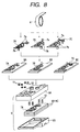
- One of the aforementioned electric connection boxes is manufactured, as shown in Fig. 8, by punching a hoop material 6 into individual bus bars 7A to 7C by a press mold, by cutting and raising tab terminals 7a and 7b vertically from the pattern portion of each of the bus bars 7A to 7C, by stacking insulating plates 8A to 8C individually between the bus bars 7A to 7C, and by housing the stack in an upper case 9A and a lower case 9B of an electric connection box 9.
- numeral 10 designates relay terminals
- numerals 11 and 12 designate relays and fuses.
- bus bars 7A to 7C have pattern portions of different shapes, however, they have to be individually punched out by dedicated press molds so that their fabrication costs rise. If the electric connection boxes of the same kind of automobile belong to different grades, the pattern portions of the bus bars have different shapes to raise another problem of lack of flexibility.
- the present invention has been conceived to solve the aforementioned problems of the prior art and has an object to provide a bus bar connection structure which can lower the fabrication cost and which is excellent in the flexibility.
- connection structure for bus bars to be housed in an electric connection box characterized: in that there are arranged on one side of an insulating plate longitudinal bus bars which are extended straight in a longitudinal direction at a predetermined pitch whereas there are arranged on the other face of the insulating plate transverse bus bars which are extended straight in a transverse direction at a predetermined pitch; in that the insulating plate is provided with through holes at the intersecting portions of the bus bars on the two faces; in that at least one of the bus bars on the two faces is provided at suitable positions of the intersecting portions with recesses to be fitted in the through holes; and in that the recesses are brought into contact with and welded to the bus bars on the confronting face so that the bus bars on the two faces are electrically connected.
- the bus bars on the two faces can be electrically connected by arranging the longitudinal bus bars on one face of the insulating plate and the transverse bus bars on the other face of the insulating plate, by fitting the recesses of at least one of the bus bars of the suitable positions of the intersecting portions of the bus bars on the two faces in the through holes of the insulating plate, and by bringing the recesses into contact with the face, as confronted thereby, and welding them to the confronted face.
- Another circuit can be formed by making an electric disconnection with the same bus bars.
- the construction can be made, as in Aspect 4, such that the bus bars for the lower layer are provided with lower layer compression blades which are extended through slits formed in said insulating plate to over the face of the insulating plate for the upper layer, such that there are arranged on the face of the insulating plate for the upper layer the bus bars which are provided at their two ends with upper layer compression blades confronting the lower layer compression blades and connector tab terminals, and such that jumper electric wires are compressed on the upper layer compression blades and the lower layer compression blades to connect the bus bars on the two faces electrically.
- the construction can be made, as in Aspect 5, such that the bus bars for the lower layer are provided with lower layer compression blades which are extended through slits formed in said insulating plate to over the face of the insulating plate for the upper layer, such that there are arranged on the face of the insulating plate for the upper layer connector tab terminals which are provided with compression blades at their lower ends, and such that jumper electric wires are compressed on the compression blades and the lower layer compression blades so that the bus bars for the lower layer and the connector tab terminals for the upper layer are electrically connected.
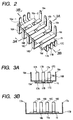
- a rectangular insulating plate 15 On the lower face of a rectangular insulating plate 15, as shown in Figs. 1 to 3, there are arranged longitudinal bus bars 17A, 17B and 17C which are extended straight in the longitudinal direction at a predetermined pitch P1.
- transverse bus bars 16A, 16B, 16C and 16D On the upper face of the insulating plate 15, there are arranged transverse bus bars 16A, 16B, 16C and 16D which are extended straight in the transverse direction at a predetermined pitch P2.
- through holes 15a are formed in a lattice shape in all the intersections of the bus bars 16(A to C) and 17(A to D) on the two faces.
- bus bar grooves 15b are formed in the lower face of the insulating plate 15, for fitting the longitudinal bus bars 17 (A to C) individually.
- a recess 16a-1 of the transverse bus bar 16A contacts with the longitudinal bus bar 17A
- a recess 16a-2 of the contacts with the longitudinal bus bar 17C Likewise: the recess 16b of the transverse bus bar 16B contacts with the longitudinal bus bar 17b; the recess 16c of the transverse bus bar 16C contacts with the longitudinal bus bar 17C; and the recess 16d of the transverse bus bar 16D contacts with the longitudinal bus bar 17A.
- the individual recesses 16a to 16d of the transverse bus bars 16 (A to D) are electrically connected with the individual opposed longitudinal bus bars 17 (A to C) by welding their contacting portions individually by means of a laser.
- transverse bus bars 16(A to D) and longitudinal bus bars 17(A to C) are raised upward to form connector tab terminals 16e and 17e.
- the transverse bus bar 16A is cut between the recesses 16a-1 and 16a-2 so that it can be disconnected.
- the bus bars 16 (A to D) and 17(A to C) on the upper and lower faces of the insulating plate 15 can be electrically connected by arranging the transverse bus bars 16(A to D) on the upper face of the insulating plate 15 and the longitudinal bus bars 17(A to C) on the lower face of the insulating plate, by fitting the recesses 16a to 16d of the transverse bus bars 16(A to D) in the through holes 15a of the insulating plate 15 to weld them to the opposed longitudinal bus bars 17(A to C).
- the insulating plate 15 and the longitudinal bus bars 17(A to C) can be made completely common, and the transverse bus bars 16(A to D) can also be made common by forming the positions of the recesses 16a to 16d later.
- the bus bar structure is made merely by arranging those straight longitudinal bus bars 17(A to C) and transverse bus bars 16(A to D) in combination, and by welding the recesses 16a to 16d at the intersecting portions.
- the bus bars need not be punched into different pattern shapes by dedicated press molds, as in the prior art, thereby to lower the fabrication cost.
- the structure can respond to any bus bar pattern shape to reduce the number of steps of designing the circuit remarkably and to respond a design change accompanying a slight circuit change quickly thereby to improve the flexibility drastically.
- connector tab terminals 16e and 17e are individually formed at the two end portions of the individual bus bars 16(A to D) and 17(A to C), moreover, they need not be separately welded so that the fabrication cost is lowered.
- transverse bus bar 16A is cut so that even an identical bus bar can be electrically disconnected to make another circuit.
- the transverse bus bars 16(A to D) are provided with the recesses 16a to 16d.
- the longitudinal bus bars 17(A to C) may be provided with recesses and welded to the transverse bus bars 16(A to D).
- the transverse bus bars 16(A to D) and the longitudinal bus bars 17(A to C) may be individually provided with recesses, and these recesses may be welded in the through holes 15a.
- Fig. 4 to Fig. 6A show a first application embodiment, in which transverse bus bars 16F and 16G are basically given the same shape as that of the aforementioned transverse bus bars 16(A to D).
- longitudinal bus bars 17F to 17H are also basically given the same shape as that of the aforementioned longitudinal bus bars 17(A to C).
- lower layer compression blades 17i are formed integrally with the side edge portions of the longitudinal bus bars 17F to 17H and are raised upward, as shown in Fig. 6A, like the connector tab terminals 17e.
- the lower layer compression blades 17i other than the necessary ones are cut off by means of a press.
- the longitudinal bus bars 17F to 17H can spare their own material to improve the yield, if they are blanked to stagger the lower layer compression blades 17i.
- recesses 16f and 16g of the aforementioned individual transverse bus bars 16(F, G) are fitted in the through holes 15a of the insulating plate 15 and are individually brought into contact with the opposed longitudinal bus bars 17(F to H), so that they are electrically connected by welding the contacting portions individually by means of a laser.
- jumper electric wires 19 are compressed on the upper layer compression blades 18a and the lower layer compression blades 17i so that the bus bars 18(A to F) and 17(F to H) on the upper and lower faces of the insulating plate 15 can be electrically connected with ease.
- Fig. 7 shows a second application embodiment.
- I-shaped bus bar connector tab terminals 20 (as referred to Fig. 6B) which are provided with compression blades 20a at their lower ends.
- the compression blades 20a of those individual tab terminals 20 are confronted by the lower layer compression blades 17i of the aforementioned longitudinal bus bars 17(F to H), as are extended through the (not-shown) lists formed in the aforementioned insulating plate 15 to over the upper face of the insulating plate 15.
- the jumper electric wires 19 are compressed on the compression blades 20a of the tab terminals 20 and the lower layer compression blades 17i of the longitudinal bus bars 17(F to H) so that the tab terminals 20 on the upper face of the insulating plate 15 and the bus bars 17(F to H) on the lower face can be electrically connected with ease.
- the bus bars on the two faces can be electrically connected by arranging the longitudinal bus bars on the one face of the insulating plate and the transverse bus bars on the other face of the insulating plate, by fitting the recesses of the bus bars of at least one face at the suitable positions of the intersecting portions of the bus bars of the two faces in the through holes of the insulating plate to bring the recesses into contact with the bus bars of the face, as confronted thereby, and to weld them to the same bus bars.
- the bus bars are made merely by arranging those common, straight longitudinal bus bars and transverse bus bars in combination, and by welding the recesses at the intersecting portions connecting the upper and lower layer bus bars. Unlike the prior art, therefore, the bus bars need not be punched into different pattern shapes by dedicated press molds, as in the prior art, thereby to lower the fabrication cost.
- the structure can respond to any bus bar pattern shape to reduce the number of steps of designing the circuit remarkably and to respond a design change accompanying a slight circuit change quickly thereby to improve the flexibility drastically.
- the bus bars for the lower layer and the bus bars for the upper layer or the connector tab terminals can be electrically connected with ease.
Landscapes
- Engineering & Computer Science (AREA)
- Microelectronics & Electronic Packaging (AREA)
- Manufacturing & Machinery (AREA)
- Connection Or Junction Boxes (AREA)
- Installation Of Bus-Bars (AREA)
- Multi-Conductor Connections (AREA)
Applications Claiming Priority (2)
| Application Number | Priority Date | Filing Date | Title |
|---|---|---|---|
| JP18064999A JP3338004B2 (ja) | 1999-06-25 | 1999-06-25 | バスバーの接続構造 |
| JP18064999 | 1999-06-25 |
Publications (3)
| Publication Number | Publication Date |
|---|---|
| EP1065768A2 true EP1065768A2 (de) | 2001-01-03 |
| EP1065768A3 EP1065768A3 (de) | 2003-01-15 |
| EP1065768B1 EP1065768B1 (de) | 2006-02-08 |
Family
ID=16086898
Family Applications (1)
| Application Number | Title | Priority Date | Filing Date |
|---|---|---|---|
| EP00105142A Expired - Lifetime EP1065768B1 (de) | 1999-06-25 | 2000-03-10 | Verbindungsstruktur für Stromsammelschienen |
Country Status (4)
| Country | Link |
|---|---|
| US (1) | US6270361B1 (de) |
| EP (1) | EP1065768B1 (de) |
| JP (1) | JP3338004B2 (de) |
| DE (1) | DE60025859T2 (de) |
Cited By (6)
| Publication number | Priority date | Publication date | Assignee | Title |
|---|---|---|---|---|
| EP1335452A3 (de) * | 2002-02-08 | 2007-05-02 | W.C. Heraeus GmbH | Verfahren zur elektrischen Kontaktierung zweier Metallstrukturen |
| DE102007003652A1 (de) * | 2007-01-18 | 2008-07-31 | Tyco Electronics Amp Gmbh | Elektrische Überbrückung |
| EP2913229A1 (de) * | 2009-09-03 | 2015-09-02 | Lisa Dräxlmaier GmbH | Elektrisches bauteil als halbzeug für einen stromverteiler |
| WO2017071815A1 (de) * | 2015-10-27 | 2017-05-04 | Sew-Eurodrive Gmbh & Co. Kg | Anschlusseinheit für ein elektrogerät, elektrogerätesystem und verfahren zur herstellung |
| DE102004061527B4 (de) | 2003-12-22 | 2018-08-16 | Kabushiki Kaisha T An T | Stromschienenträger für eine Innenleuchte eines Fahrzeugs |
| US20210328396A1 (en) * | 2018-08-27 | 2021-10-21 | Molex, Llc | Hinged busbar assembly |
Families Citing this family (20)
| Publication number | Priority date | Publication date | Assignee | Title |
|---|---|---|---|---|
| JP2001035616A (ja) * | 1999-07-21 | 2001-02-09 | Sumitomo Wiring Syst Ltd | ワイヤハーネス用ジョイントコネクタ |
| JP3446672B2 (ja) * | 1999-07-30 | 2003-09-16 | 住友電装株式会社 | 電気接続箱 |
| JP4097388B2 (ja) * | 2000-07-21 | 2008-06-11 | 住友電装株式会社 | ジャンクションボックスの組立方法および該方法で組み立てられたジャンクションボックス |
| EP1201505B1 (de) * | 2000-10-26 | 2006-12-06 | Sumitomo Wiring Systems, Ltd. | Elektrische Kraftfahrzeugverbindungsdose |
| JP3724372B2 (ja) * | 2000-12-28 | 2005-12-07 | 住友電装株式会社 | 電気接続箱 |
| DE10117798A1 (de) * | 2001-04-10 | 2002-12-05 | Bosch Gmbh Robert | Stecker |
| KR100440159B1 (ko) * | 2002-06-26 | 2004-07-12 | 현대자동차주식회사 | 차량의 릴레이 박스 |
| JP4580036B1 (ja) * | 2009-06-12 | 2010-11-10 | 株式会社神戸製鋼所 | バスバーおよびコネクタ |
| US8379374B2 (en) * | 2010-07-16 | 2013-02-19 | Rockwell Automation Technologies, Inc. | Bus to bus power interconnect |
| DE102011004526B4 (de) | 2011-02-22 | 2021-05-06 | Vitesco Technologies GmbH | Leiterplatte mit hoher Stromtragfähigkeit und Verfahren zur Herstellung einer solchen Leiterplatte |
| JP6000722B2 (ja) * | 2012-07-30 | 2016-10-05 | ユニオンマシナリ株式会社 | 成形配線板ユニット |
| JP6078410B2 (ja) * | 2013-04-12 | 2017-02-08 | 矢崎総業株式会社 | 電子部品の組付構造及び電子部品 |
| US9391413B2 (en) * | 2013-04-23 | 2016-07-12 | Abb Technology Ag | Bus bar arrangement and a shroud for the same |
| US9917291B2 (en) | 2015-05-05 | 2018-03-13 | Johnson Controls Technology Company | Welding process for a battery module |
| US9812848B2 (en) * | 2015-10-30 | 2017-11-07 | Rockwell Automation Technologies, Inc. | Fixed vertical distribution bus bar |
| KR101989859B1 (ko) * | 2016-12-15 | 2019-09-30 | 주식회사 아모그린텍 | 파워 릴레이 어셈블리 |
| EP3454436B1 (de) * | 2017-09-11 | 2024-07-17 | ABB S.p.A. | Fachaufteilungs- und sammelschienenunterstützungsvorrichtung in einem niederspannungsschaltschrank |
| JP6835795B2 (ja) * | 2018-11-12 | 2021-02-24 | 矢崎総業株式会社 | バスバー押さえ構造、電気接続箱、及びワイヤハーネス |
| DE102018219466A1 (de) * | 2018-11-14 | 2020-05-14 | Audi Ag | Verfahren zum Herstellen einer Stromführungseinrichtung, Anschlussdose für eine Fahrzeugbatterie und Kraftfahrzeug |
| JP7803692B2 (ja) * | 2021-11-24 | 2026-01-21 | 古河電気工業株式会社 | 電気接続体及び電気接続体の製造方法 |
Family Cites Families (10)
| Publication number | Priority date | Publication date | Assignee | Title |
|---|---|---|---|---|
| US2019625A (en) * | 1934-03-30 | 1935-11-05 | Rca Corp | Electrical apparatus |
| US2977672A (en) * | 1958-12-12 | 1961-04-04 | Gen Electric | Method of making bonded wire circuit |
| US4208080A (en) * | 1976-08-18 | 1980-06-17 | Amp Incorporated | Junction boxes |
| JPS6035911A (ja) * | 1983-08-05 | 1985-02-23 | 古河電気工業株式会社 | 電気接続箱 |
| US4963099A (en) * | 1988-03-25 | 1990-10-16 | Yazaki Corporation | Electrical junction box |
| JPH0615457Y2 (ja) * | 1988-07-15 | 1994-04-20 | 矢崎総業株式会社 | 電気接続箱 |
| US5295847A (en) * | 1990-01-16 | 1994-03-22 | Yazaki Corporation | Branch junction box and busbars for branch connection |
| US5310353A (en) * | 1992-06-17 | 1994-05-10 | Augat Inc. | Electrical power distribution center having conductive ridges |
| JP2929414B2 (ja) * | 1994-07-05 | 1999-08-03 | 矢崎総業株式会社 | 電気接続箱 |
| US5801335A (en) * | 1997-03-28 | 1998-09-01 | General Motors Corporation | Swage lock for coupling substrates together |
-
1999
- 1999-06-25 JP JP18064999A patent/JP3338004B2/ja not_active Expired - Fee Related
-
2000
- 2000-03-07 US US09/520,186 patent/US6270361B1/en not_active Expired - Fee Related
- 2000-03-10 DE DE60025859T patent/DE60025859T2/de not_active Expired - Lifetime
- 2000-03-10 EP EP00105142A patent/EP1065768B1/de not_active Expired - Lifetime
Cited By (11)
| Publication number | Priority date | Publication date | Assignee | Title |
|---|---|---|---|---|
| EP1335452A3 (de) * | 2002-02-08 | 2007-05-02 | W.C. Heraeus GmbH | Verfahren zur elektrischen Kontaktierung zweier Metallstrukturen |
| DE102004061527B4 (de) | 2003-12-22 | 2018-08-16 | Kabushiki Kaisha T An T | Stromschienenträger für eine Innenleuchte eines Fahrzeugs |
| DE102007003652A1 (de) * | 2007-01-18 | 2008-07-31 | Tyco Electronics Amp Gmbh | Elektrische Überbrückung |
| DE102007003652B4 (de) * | 2007-01-18 | 2014-05-28 | Tyco Electronics Amp Gmbh | Elektrische Überbrückung |
| EP2913229A1 (de) * | 2009-09-03 | 2015-09-02 | Lisa Dräxlmaier GmbH | Elektrisches bauteil als halbzeug für einen stromverteiler |
| WO2017071815A1 (de) * | 2015-10-27 | 2017-05-04 | Sew-Eurodrive Gmbh & Co. Kg | Anschlusseinheit für ein elektrogerät, elektrogerätesystem und verfahren zur herstellung |
| CN107851912A (zh) * | 2015-10-27 | 2018-03-27 | 索尤若驱动有限及两合公司 | 用于电气设备的接线单元、电气设备系统和制造方法 |
| US20180316148A1 (en) * | 2015-10-27 | 2018-11-01 | Sew-Eurodrive Gmbh & Co. Kg | Connection unit for an electrical device, electrical device system, and production method |
| US10594098B2 (en) | 2015-10-27 | 2020-03-17 | Sew-Eurodrive Gmbh & Co. Kg | Connection unit for an electrical device, electrical device system, and production method |
| US20210328396A1 (en) * | 2018-08-27 | 2021-10-21 | Molex, Llc | Hinged busbar assembly |
| US11837830B2 (en) * | 2018-08-27 | 2023-12-05 | Molex, Llc | Hinged busbar assembly |
Also Published As
| Publication number | Publication date |
|---|---|
| JP3338004B2 (ja) | 2002-10-28 |
| EP1065768A3 (de) | 2003-01-15 |
| US6270361B1 (en) | 2001-08-07 |
| EP1065768B1 (de) | 2006-02-08 |
| DE60025859T2 (de) | 2006-09-28 |
| JP2001016745A (ja) | 2001-01-19 |
| DE60025859D1 (de) | 2006-04-20 |
Similar Documents
| Publication | Publication Date | Title |
|---|---|---|
| EP1065768B1 (de) | Verbindungsstruktur für Stromsammelschienen | |
| EP1017133A2 (de) | Elektrisches Verbindergehäuse | |
| US6514091B2 (en) | Electrical junction box for a vehicle | |
| EP0994639B1 (de) | Gitterleiterplatte | |
| US6390830B1 (en) | Bus bar-connecting structure | |
| US8258913B2 (en) | Fuse element and method of manufacturing the same | |
| JP3446672B2 (ja) | 電気接続箱 | |
| EP1063725B1 (de) | Verbindungsstruktur für elektrische Drähte | |
| EP1119225B1 (de) | Gedruckte Schaltungsplatte, elektrisches Verbindungsgehäuse mit dieser Schaltungsplatte und Verfahren zur Herstellung | |
| US20010031583A1 (en) | Multipole electrical connector | |
| JP2000307202A (ja) | 回路板および該回路板を収容した電気接続箱 | |
| US6626693B2 (en) | Metal terminal and method of forming metal terminal | |
| JP3562431B2 (ja) | 大型バスバーの製造方法 | |
| EP1283578A1 (de) | Verbinder ausgestattet mit Klammerkontakten auf einer Sammelschiene | |
| JP3501056B2 (ja) | 電気接続箱 | |
| EP0895310A2 (de) | Elektrische Anschlussbuchse und Herstellungsverfahren für die Endanschlüsse | |
| JP3427780B2 (ja) | 回路板を収容した電気接続箱 | |
| JPH07135719A (ja) | バスバー材料、該バスバー材料より形成されるバスバー及び該バスバーを備えた電気接続箱 | |
| JP3736341B2 (ja) | ジャンクションボックス内に収容する回路板の形成方法および回路板を収容しているジャンクションボックス | |
| JP2001314020A (ja) | 電気接続箱及びそれに用いるブスバーの形成方法 | |
| JP3364881B2 (ja) | ブスバー配線板の製造方法 | |
| JPH11215655A (ja) | 電気接続箱のバスバー構造 | |
| JP2007215373A (ja) | 自動車用ジャンクションボックス | |
| KR19980084250A (ko) | 자동차의 역전류방지용 다이오드 제조방법 | |
| JP2008022682A (ja) | ジャンクションブロック |
Legal Events
| Date | Code | Title | Description |
|---|---|---|---|
| PUAI | Public reference made under article 153(3) epc to a published international application that has entered the european phase |
Free format text: ORIGINAL CODE: 0009012 |
|
| AK | Designated contracting states |
Kind code of ref document: A2 Designated state(s): AT BE CH CY DE DK ES FI FR GB GR IE IT LI LU MC NL PT SE |
|
| AX | Request for extension of the european patent |
Free format text: AL;LT;LV;MK;RO;SI |
|
| PUAL | Search report despatched |
Free format text: ORIGINAL CODE: 0009013 |
|
| AK | Designated contracting states |
Kind code of ref document: A3 Designated state(s): AT BE CH CY DE DK ES FI FR GB GR IE IT LI LU MC NL PT SE |
|
| AX | Request for extension of the european patent |
Free format text: AL;LT;LV;MK;RO;SI |
|
| RIC1 | Information provided on ipc code assigned before grant |
Free format text: 7H 02B 1/20 A, 7H 01R 25/16 B, 7H 02G 5/00 B, 7H 05K 7/02 B, 7H 01R 9/22 B |
|
| RAP1 | Party data changed (applicant data changed or rights of an application transferred) |
Owner name: SUMITOMO ELECTRIC INDUSTRIES, LTD. Owner name: SUMITOMO WIRING SYSTEMS, LTD. Owner name: AUTONETWORKS TECHNOLOGIES, LTD. |
|
| 17P | Request for examination filed |
Effective date: 20030320 |
|
| 17Q | First examination report despatched |
Effective date: 20030812 |
|
| AKX | Designation fees paid |
Designated state(s): DE |
|
| GRAP | Despatch of communication of intention to grant a patent |
Free format text: ORIGINAL CODE: EPIDOSNIGR1 |
|
| GRAS | Grant fee paid |
Free format text: ORIGINAL CODE: EPIDOSNIGR3 |
|
| GRAA | (expected) grant |
Free format text: ORIGINAL CODE: 0009210 |
|
| AK | Designated contracting states |
Kind code of ref document: B1 Designated state(s): DE |
|
| REF | Corresponds to: |
Ref document number: 60025859 Country of ref document: DE Date of ref document: 20060420 Kind code of ref document: P |
|
| PLBE | No opposition filed within time limit |
Free format text: ORIGINAL CODE: 0009261 |
|
| STAA | Information on the status of an ep patent application or granted ep patent |
Free format text: STATUS: NO OPPOSITION FILED WITHIN TIME LIMIT |
|
| 26N | No opposition filed |
Effective date: 20061109 |
|
| PGFP | Annual fee paid to national office [announced via postgrant information from national office to epo] |
Ref country code: DE Payment date: 20130306 Year of fee payment: 14 |
|
| REG | Reference to a national code |
Ref country code: DE Ref legal event code: R119 Ref document number: 60025859 Country of ref document: DE |
|
| REG | Reference to a national code |
Ref country code: DE Ref legal event code: R119 Ref document number: 60025859 Country of ref document: DE Effective date: 20141001 |
|
| PG25 | Lapsed in a contracting state [announced via postgrant information from national office to epo] |
Ref country code: DE Free format text: LAPSE BECAUSE OF NON-PAYMENT OF DUE FEES Effective date: 20141001 |