EP1065788A2 - Convertisseur analogique-numérique et codeur correspondant - Google Patents
Convertisseur analogique-numérique et codeur correspondant Download PDFInfo
- Publication number
- EP1065788A2 EP1065788A2 EP00119883A EP00119883A EP1065788A2 EP 1065788 A2 EP1065788 A2 EP 1065788A2 EP 00119883 A EP00119883 A EP 00119883A EP 00119883 A EP00119883 A EP 00119883A EP 1065788 A2 EP1065788 A2 EP 1065788A2
- Authority
- EP
- European Patent Office
- Prior art keywords
- signal
- output
- signals
- circuit
- input
- Prior art date
- Legal status (The legal status is an assumption and is not a legal conclusion. Google has not performed a legal analysis and makes no representation as to the accuracy of the status listed.)
- Granted
Links
Images











Classifications
-
- H—ELECTRICITY
- H03—ELECTRONIC CIRCUITRY
- H03M—CODING; DECODING; CODE CONVERSION IN GENERAL
- H03M1/00—Analogue/digital conversion; Digital/analogue conversion
- H03M1/12—Analogue/digital converters
- H03M1/34—Analogue value compared with reference values
- H03M1/36—Analogue value compared with reference values simultaneously only, i.e. parallel type
-
- H—ELECTRICITY
- H03—ELECTRONIC CIRCUITRY
- H03M—CODING; DECODING; CODE CONVERSION IN GENERAL
- H03M7/00—Conversion of a code where information is represented by a given sequence or number of digits to a code where the same, similar or subset of information is represented by a different sequence or number of digits
- H03M7/14—Conversion to or from non-weighted codes
- H03M7/16—Conversion to or from unit-distance codes, e.g. Gray code, reflected binary code
- H03M7/165—Conversion to or from thermometric code
-
- H—ELECTRICITY
- H03—ELECTRONIC CIRCUITRY
- H03M—CODING; DECODING; CODE CONVERSION IN GENERAL
- H03M1/00—Analogue/digital conversion; Digital/analogue conversion
- H03M1/12—Analogue/digital converters
- H03M1/34—Analogue value compared with reference values
- H03M1/36—Analogue value compared with reference values simultaneously only, i.e. parallel type
- H03M1/361—Analogue value compared with reference values simultaneously only, i.e. parallel type having a separate comparator and reference value for each quantisation level, i.e. full flash converter type
- H03M1/362—Analogue value compared with reference values simultaneously only, i.e. parallel type having a separate comparator and reference value for each quantisation level, i.e. full flash converter type the reference values being generated by a resistive voltage divider
- H03M1/365—Analogue value compared with reference values simultaneously only, i.e. parallel type having a separate comparator and reference value for each quantisation level, i.e. full flash converter type the reference values being generated by a resistive voltage divider the voltage divider being a single resistor string
Definitions
- the output signals SG1-SG3 are supplied to the encoder section 3 from the comparators CM1-CM3.
- the operation timings of the comparators CM1-CM3 and the encoder section 3 are controlled by the control circuit 4.
- the address decoder and the encoder section 3 output digital output signals D0 and D1, each consisting of a single bit.
- An A/D converter embodying a second aspect of the present invention includes a plurality of comparators, an address decoder and an encoder section. Those comparators receive reference voltages respectively having different voltage values. Each comparator compares the received reference voltage with an analog input voltage and produces an output according to a thermometer code.
- the address decoder outputs an address signal for selecting a specific address based on the output signals of the comparators.
- the encoder section includes a plurality of ROM cells connected between a plurality of bit lines and a plurality of word lines. In response to the selection of a word line, the ROM cells permit a digital signal associated with the selected word line to be output from the bit lines.
- the control circuit 31 allows the comparators CM which are equal in number to the number of thermometer-code based outputs to perform the comparison operation and allows the remaining comparators CM to perform the reset operation.
- the first selector 44 selects the output signals from the comparators CM which are executing the comparison operation, and sends the selected output signals to the encoder 32 as thermometer-code based outputs.
- the second selector 45 selects the reference voltages which are to be supplied to the comparators that execute the reset operation in such a way that the combination of the reference voltages to be supplied to the comparators which execute the comparison operation always becomes the same.
- the reset operation based on the reference voltages and the comparison between an analog voltage with the reference voltages are executed in parallel.
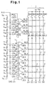
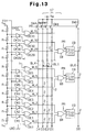
- the number of the ROM cells 2 connected to the least significant bit line BL0 is half the number required by the first previously-considered A/D converter. Therefore, the parasitic capacitance of the bit line BL0 becomes smaller than that of the first previously-considered A/D converter. Since the precharge potential of the least significant bit line BL0 is the most frequently inverted, the reduction of the parasitic capacitance of bit line BL0 therefore significantly contributes to increasing the operation speed of the encoder section 17. As such, the operation speed of the entire A/D converter is improved by the increased operation speed of the encoder section 17. This advantage becomes more pronounced as the number of bits of a digital output signal increases, which requires that the number of ROM cells 2 connected to bit line BL0 be increased.
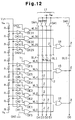
- the least significant bit line BL0 consists of two bit lines BL0a and BL0b.
- a group of ROM cells are alternately connected to the two bit lines BL0a and BL0b.
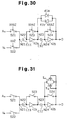
- the switch circuit S16 is controlled by a reset signal XXAZ. More specifically, when the reset signal XXAZ goes high, the switch circuit S16 is turned on to apply the reference voltage V R to the capacitor C2, while when the reset signal XXAZ goes low, the switch circuit S16 is turned off.
- the comparator CM2 When the reset signal XAZ2 goes low next, the comparator CM2 initiates the reset operation. Because of the H-level control signal XUD, the comparator CM2 is reset by the reference voltage V R2 . Further, the control signal N3 goes low so that the comparator CM3 outputs the output signal Q3 as the output signal E3. Therefore, the comparators CM0, CM1 and CM3 compare the analog input signal Ain with the reference voltages V R1 to V R3 and output the output signals Q0, Q1 and Q3 indicative of the comparison results as the output signals E1-E3.
- the comparator CM0 When the reset signal XAZ0 goes low next, the comparator CM0 initiates the reset operation. Because of the H-level control signal XUD, the comparator CM1 is reset by the reference voltage V RL . Further, the control signal N1 goes low so that the comparator CM1 outputs the output signal Q1 as the output signal E1. Therefore, the comparators CM1, CM2 and CM3 compare the analog input signal Ain with the reference voltages V R1 to V R3 and output the output signals Q1, Q2 and Q3 indicative of the comparison results as the output signals E1-E3.
- the IAZ architecture is defined that each comparator in turn is auto-zeroed while the others stay in the comparison state, but as a whole the A/D converter always appears to be in the comparison state.
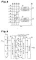
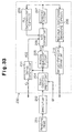
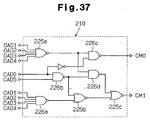
- a register 221 for use in setting the compensation amount, holds the value of an 8-bit binary code in the D/A converter 217, which corresponds to a one-LSB change in the potential of each of the digital output signals OAD0-OAD4 from the A/D converter 215.
- a write control signal WRITE and an address signal ADR are input to the register 221 from an external MPU via a serial interface 220, externally supplied data is written, via data bus DBUS, to an address in the register 221 which is selected by the address signal ADR.
- the data stored in the register 221 can be erased by a reset signal XRESET externally supplied thereto.
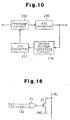
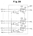
- the LSB selecting circuit 222 When the control signals LBC and LBD both go high, the LSB selecting circuit 222 directly outputs the input data I7-I0 as the eight 1-bit output signals OT7-OT0.
- the control signal LBC goes low with the control signal LBD kept high, the LSB selecting circuit 222 shifts the input data I7-I2 by two bits to the least significant bit side and outputs the resultant data as the output signals OT5-OT0. In this case, the output signals OT7 and OT6 are set to "0".
- the switch circuit 212 when the reading of the servo area by the reading head 201 starts, the switch circuit 212 is turned off to inhibit the inputting of the analog input signal Ain, so that the closed loop circuit is formed by the amplifier 214, A/D converter 215, offset voltage canceling circuit 216, D/A converter 217 and resistors R1-R3.
- the offset voltage of the A/D converter 215 can be therefore automatically canceled by the action of the offset voltage canceling circuit 216.
Landscapes
- Engineering & Computer Science (AREA)
- Theoretical Computer Science (AREA)
- Analogue/Digital Conversion (AREA)
Applications Claiming Priority (7)
| Application Number | Priority Date | Filing Date | Title |
|---|---|---|---|
| JP3407695 | 1995-02-22 | ||
| JP3407695 | 1995-02-22 | ||
| JP20622695A JP3579138B2 (ja) | 1995-08-11 | 1995-08-11 | 半導体集積回路 |
| JP20622695 | 1995-08-11 | ||
| JP23175795 | 1995-09-08 | ||
| JP7231757A JP2945307B2 (ja) | 1995-02-22 | 1995-09-08 | A/d変換器 |
| EP96301186A EP0729235B1 (fr) | 1995-02-22 | 1996-02-22 | Convertisseurs analogiques-numériques et codeur pour de tels convertisseurs |
Related Parent Applications (1)
| Application Number | Title | Priority Date | Filing Date |
|---|---|---|---|
| EP96301186A Division EP0729235B1 (fr) | 1995-02-22 | 1996-02-22 | Convertisseurs analogiques-numériques et codeur pour de tels convertisseurs |
Publications (3)
| Publication Number | Publication Date |
|---|---|
| EP1065788A2 true EP1065788A2 (fr) | 2001-01-03 |
| EP1065788A3 EP1065788A3 (fr) | 2002-01-23 |
| EP1065788B1 EP1065788B1 (fr) | 2004-11-24 |
Family
ID=27288320
Family Applications (2)
| Application Number | Title | Priority Date | Filing Date |
|---|---|---|---|
| EP00119883A Expired - Lifetime EP1065788B1 (fr) | 1995-02-22 | 1996-02-22 | Convertisseur analogique-numérique et codeur correspondant |
| EP96301186A Expired - Lifetime EP0729235B1 (fr) | 1995-02-22 | 1996-02-22 | Convertisseurs analogiques-numériques et codeur pour de tels convertisseurs |
Family Applications After (1)
| Application Number | Title | Priority Date | Filing Date |
|---|---|---|---|
| EP96301186A Expired - Lifetime EP0729235B1 (fr) | 1995-02-22 | 1996-02-22 | Convertisseurs analogiques-numériques et codeur pour de tels convertisseurs |
Country Status (5)
| Country | Link |
|---|---|
| US (2) | US6288668B1 (fr) |
| EP (2) | EP1065788B1 (fr) |
| KR (1) | KR100215137B1 (fr) |
| DE (2) | DE69633945T2 (fr) |
| TW (1) | TW282598B (fr) |
Families Citing this family (31)
| Publication number | Priority date | Publication date | Assignee | Title |
|---|---|---|---|---|
| JP3439322B2 (ja) * | 1997-06-17 | 2003-08-25 | Necエレクトロニクス株式会社 | 差動入力チョッパ型電圧比較回路 |
| US6218975B1 (en) * | 1997-09-02 | 2001-04-17 | Fujitsu Limited | Interleaved auto-zero analog-to-digital converter with switching noise compensation |
| JP2001319424A (ja) * | 1999-09-24 | 2001-11-16 | Sanyo Electric Co Ltd | 信号処理回路および半導体集積回路 |
| KR100725881B1 (ko) * | 1999-09-24 | 2007-06-08 | 산요덴키가부시키가이샤 | 신호 처리 회로 및 반도체 집적 회로 |
| US7173551B2 (en) | 2000-12-21 | 2007-02-06 | Quellan, Inc. | Increasing data throughput in optical fiber transmission systems |
| US7149256B2 (en) | 2001-03-29 | 2006-12-12 | Quellan, Inc. | Multilevel pulse position modulation for efficient fiber optic communication |
| US7307569B2 (en) | 2001-03-29 | 2007-12-11 | Quellan, Inc. | Increasing data throughput in optical fiber transmission systems |
| CA2442922A1 (fr) | 2001-04-04 | 2002-10-17 | Quellan, Inc. | Procede et systeme permettant de decoder des signaux multiniveau |
| AU2003211094A1 (en) | 2002-02-15 | 2003-09-09 | Quellan, Inc. | Multi-level signal clock recovery technique |
| US6816101B2 (en) * | 2002-03-08 | 2004-11-09 | Quelian, Inc. | High-speed analog-to-digital converter using a unique gray code |
| EP1367720B1 (fr) * | 2002-05-27 | 2007-06-13 | Fujitsu Limited | Circuit de courant de polarisation de convertisseur A/N |
| US7035361B2 (en) | 2002-07-15 | 2006-04-25 | Quellan, Inc. | Adaptive noise filtering and equalization for optimal high speed multilevel signal decoding |
| AU2003287628A1 (en) | 2002-11-12 | 2004-06-03 | Quellan, Inc. | High-speed analog-to-digital conversion with improved robustness to timing uncertainty |
| US7804760B2 (en) | 2003-08-07 | 2010-09-28 | Quellan, Inc. | Method and system for signal emulation |
| WO2005018134A2 (fr) | 2003-08-07 | 2005-02-24 | Quellan, Inc. | Procede et systeme pour supprimer la diaphonie |
| ATE488068T1 (de) | 2003-11-17 | 2010-11-15 | Quellan Inc | Verfahren und system zur löschung von antennenstörungen |
| US7616700B2 (en) | 2003-12-22 | 2009-11-10 | Quellan, Inc. | Method and system for slicing a communication signal |
| JP2005269400A (ja) * | 2004-03-19 | 2005-09-29 | Sanyo Electric Co Ltd | 比較装置及び方法、その比較方法を利用可能なアナログデジタル変換装置、及びその比較方法に利用可能な判定装置 |
| US7522883B2 (en) | 2004-12-14 | 2009-04-21 | Quellan, Inc. | Method and system for reducing signal interference |
| US7725079B2 (en) | 2004-12-14 | 2010-05-25 | Quellan, Inc. | Method and system for automatic control in an interference cancellation device |
| JP4684743B2 (ja) * | 2005-05-27 | 2011-05-18 | ルネサスエレクトロニクス株式会社 | A/d変換回路、a/d変換器およびサンプリングクロックのスキュー調整方法 |
| KR101372361B1 (ko) | 2006-04-26 | 2014-03-12 | 인터실 아메리카스 엘엘씨 | 통신 채널로부터 복사성 방출을 감소시키기 위한 방법 및 시스템 |
| WO2008069144A1 (fr) * | 2006-12-04 | 2008-06-12 | Panasonic Corporation | Convertisseur a/n |
| JP2008219761A (ja) | 2007-03-07 | 2008-09-18 | Nec Electronics Corp | 入力信号検出回路 |
| US7696916B2 (en) * | 2007-09-13 | 2010-04-13 | Sony Corporation | Parallel type analog-to-digital conversion circuit, sampling circuit and comparison amplification circuit |
| JP4777444B2 (ja) * | 2009-03-03 | 2011-09-21 | シャープ株式会社 | デコーダ装置および移動制御装置 |
| KR101591339B1 (ko) * | 2009-08-11 | 2016-02-03 | 삼성전자주식회사 | 다단 증폭 회로 |
| JP5625857B2 (ja) * | 2010-06-10 | 2014-11-19 | 富士通株式会社 | 半導体集積回路、閾値設定方法、及び通信装置 |
| US10848166B1 (en) | 2019-12-06 | 2020-11-24 | Analog Devices International Unlimited Company | Dual mode data converter |
| US11374559B2 (en) * | 2020-05-18 | 2022-06-28 | Nxp Usa, Inc. | Low power comparator |
| KR20230089441A (ko) * | 2021-12-13 | 2023-06-20 | 주식회사 스카이칩스 | 디지털 제어되는 알에프 전력증폭기 |
Family Cites Families (22)
| Publication number | Priority date | Publication date | Assignee | Title |
|---|---|---|---|---|
| JPS55118221A (en) | 1979-03-06 | 1980-09-11 | Nec Corp | Comparison circuit |
| JPS57204633A (en) | 1981-06-10 | 1982-12-15 | Toshiba Corp | Analog-to-digital converter |
| JPS59152718A (ja) | 1983-02-18 | 1984-08-31 | Hitachi Ltd | コンパレ−タ |
| JPS60213118A (ja) | 1984-04-06 | 1985-10-25 | Hitachi Ltd | 電圧比較回路 |
| JPH0758910B2 (ja) | 1985-05-27 | 1995-06-21 | 松下電器産業株式会社 | 並列型a/d変換器 |
| JPH0681050B2 (ja) | 1985-08-21 | 1994-10-12 | 株式会社日立製作所 | 並列形ad変換器 |
| EP0217009A3 (fr) * | 1985-10-04 | 1989-05-03 | Tektronix, Inc. | Encodeur pour la conversion d'un code thermomètre en un code binaire adjacent |
| JPH0693497B2 (ja) * | 1986-07-30 | 1994-11-16 | 日本電気株式会社 | 相補型mis集積回路 |
| JPS63144617A (ja) | 1986-12-08 | 1988-06-16 | Sony Corp | チヨツパ型コンパレ−タ |
| US4963874A (en) | 1987-04-28 | 1990-10-16 | Matsushita Electric Industrial Co., Ltd. | Parallel type A/D converter |
| JP2547775B2 (ja) | 1987-06-23 | 1996-10-23 | 住友電気工業株式会社 | Ofケ−ブル |
| JPS6422210A (en) | 1987-07-17 | 1989-01-25 | Sanyo Electric Co | Control circuit of electric machinery |
| JPS6444128A (en) | 1987-08-12 | 1989-02-16 | Hitachi Ltd | A/d converter |
| JP2840747B2 (ja) | 1988-05-25 | 1998-12-24 | ソニー株式会社 | ディジタル信号再生装置 |
| JP2623298B2 (ja) | 1988-06-23 | 1997-06-25 | 三菱電機株式会社 | アナログ/デジタル変換器の制御方法 |
| US5072221A (en) | 1988-08-04 | 1991-12-10 | Signal Processing Technologies, Inc. | Error limiting analog to digital converter |
| JP2844806B2 (ja) | 1990-02-28 | 1999-01-13 | ソニー株式会社 | 並列比較型a―d変換器 |
| US5184131A (en) | 1989-07-06 | 1993-02-02 | Nissan Motor Co., Ltd. | A-d converter suitable for fuzzy controller |
| EP0730351B1 (fr) | 1990-02-28 | 2001-07-25 | Sony Corporation | Convertisseur analogique-numérique intrégralement parallèle |
| JP3103657B2 (ja) | 1992-03-23 | 2000-10-30 | 松下電器産業株式会社 | 電圧保持回路及び容量結合網を有するa/d変換器 |
| JPH06132824A (ja) | 1992-10-22 | 1994-05-13 | Matsushita Electric Ind Co Ltd | 直並列型a/d変換器 |
| US5450085A (en) | 1993-08-31 | 1995-09-12 | Advanced Micro Devices, Inc. | Method and apparatus for high speed analog to digital conversion using multiplexed flash sections |
-
1995
- 1995-09-29 TW TW084110201A patent/TW282598B/zh active
-
1996
- 1996-02-21 US US08/603,607 patent/US6288668B1/en not_active Expired - Fee Related
- 1996-02-22 EP EP00119883A patent/EP1065788B1/fr not_active Expired - Lifetime
- 1996-02-22 EP EP96301186A patent/EP0729235B1/fr not_active Expired - Lifetime
- 1996-02-22 KR KR1019960004155A patent/KR100215137B1/ko not_active Expired - Fee Related
- 1996-02-22 DE DE69633945T patent/DE69633945T2/de not_active Expired - Fee Related
- 1996-02-22 DE DE69621174T patent/DE69621174T2/de not_active Expired - Fee Related
-
2000
- 2000-05-09 US US09/568,243 patent/US6288665B1/en not_active Expired - Fee Related
Also Published As
| Publication number | Publication date |
|---|---|
| EP0729235A1 (fr) | 1996-08-28 |
| DE69633945T2 (de) | 2005-04-07 |
| DE69621174T2 (de) | 2002-08-29 |
| KR100215137B1 (ko) | 1999-08-16 |
| DE69621174D1 (de) | 2002-06-20 |
| US6288665B1 (en) | 2001-09-11 |
| EP0729235B1 (fr) | 2002-05-15 |
| EP1065788A3 (fr) | 2002-01-23 |
| KR960032909A (ko) | 1996-09-17 |
| US6288668B1 (en) | 2001-09-11 |
| DE69633945D1 (de) | 2004-12-30 |
| TW282598B (fr) | 1996-08-01 |
| EP1065788B1 (fr) | 2004-11-24 |
Similar Documents
| Publication | Publication Date | Title |
|---|---|---|
| EP1065788B1 (fr) | Convertisseur analogique-numérique et codeur correspondant | |
| KR101394640B1 (ko) | 인코드 회로 및 아날로그-디지털 변환기 | |
| TWI402854B (zh) | 用於m位元記憶體單元的m+n位元程式化及m+l位元讀取 | |
| KR960012353B1 (ko) | 부호화 회로 및 이에 적용가능한 데이터 검출용 반도체 집적회로 및 다이나믹 센스앰프 | |
| US6459394B1 (en) | Multi-bank flash ADC array with uninterrupted operation during offset calibration and auto-zero | |
| KR100284522B1 (ko) | 재편성 가능한 아날로그-디지틀 변환기 | |
| US8677221B2 (en) | Partial voltage read of memory | |
| US6456527B1 (en) | Nonvolatile multilevel memory and reading method thereof | |
| WO1989011758A1 (fr) | Circuit de decodage pour convertisseurs analogiques/numeriques rapides | |
| US6169503B1 (en) | Programmable arrays for data conversions between analog and digital | |
| US5635934A (en) | Digital read channel utilizing analog-to-digital converter with offset reduction | |
| JP2009147648A (ja) | A/d変換器及び情報記録再生装置 | |
| KR19990007167A (ko) | 다중 임계값으로부터 하나의 임계값이 설정될 수 있는 반도체 메모리 장치 | |
| JPH08293795A (ja) | エンコーダ及びa/d変換器及び半導体集積回路装置 | |
| US5684486A (en) | Flash A/D converter | |
| US7185269B2 (en) | Viterbi decoding device and method for processing multi-data input into multi-data output | |
| JP3157778B2 (ja) | エンコーダ及びa/d変換器 | |
| JP2001217716A (ja) | ディジタル・システム用の効率的アナログ/ディジタル変換器並びにその方法 | |
| GB1568101A (en) | Analog-to-digital converter | |
| JP4281909B2 (ja) | A/d変換回路とそれを用いたディスク再生システム | |
| JP2008199682A (ja) | 並列型ad変換器、これを用いた信号処理回路およびこれを搭載した記録再生装置 | |
| JP2011250188A (ja) | 固体撮像装置 | |
| JP3273887B2 (ja) | 並列型a/d変換器 | |
| JP3221131B2 (ja) | アナログ/ディジタル変換回路 | |
| JP3141265B2 (ja) | アナログ/ディジタル変換回路 |
Legal Events
| Date | Code | Title | Description |
|---|---|---|---|
| PUAI | Public reference made under article 153(3) epc to a published international application that has entered the european phase |
Free format text: ORIGINAL CODE: 0009012 |
|
| AC | Divisional application: reference to earlier application |
Ref document number: 729235 Country of ref document: EP |
|
| AK | Designated contracting states |
Kind code of ref document: A2 Designated state(s): DE FR GB |
|
| PUAL | Search report despatched |
Free format text: ORIGINAL CODE: 0009013 |
|
| AK | Designated contracting states |
Kind code of ref document: A3 Designated state(s): DE FR GB |
|
| RIC1 | Information provided on ipc code assigned before grant |
Free format text: 7H 03M 7/16 A, 7H 03M 7/22 B |
|
| 17P | Request for examination filed |
Effective date: 20020429 |
|
| AKX | Designation fees paid |
Free format text: DE FR GB |
|
| 17Q | First examination report despatched |
Effective date: 20030415 |
|
| GRAP | Despatch of communication of intention to grant a patent |
Free format text: ORIGINAL CODE: EPIDOSNIGR1 |
|
| GRAS | Grant fee paid |
Free format text: ORIGINAL CODE: EPIDOSNIGR3 |
|
| GRAA | (expected) grant |
Free format text: ORIGINAL CODE: 0009210 |
|
| AC | Divisional application: reference to earlier application |
Ref document number: 0729235 Country of ref document: EP Kind code of ref document: P |
|
| AK | Designated contracting states |
Kind code of ref document: B1 Designated state(s): DE FR GB |
|
| REG | Reference to a national code |
Ref country code: GB Ref legal event code: FG4D |
|
| REF | Corresponds to: |
Ref document number: 69633945 Country of ref document: DE Date of ref document: 20041230 Kind code of ref document: P |
|
| PLBE | No opposition filed within time limit |
Free format text: ORIGINAL CODE: 0009261 |
|
| STAA | Information on the status of an ep patent application or granted ep patent |
Free format text: STATUS: NO OPPOSITION FILED WITHIN TIME LIMIT |
|
| ET | Fr: translation filed | ||
| 26N | No opposition filed |
Effective date: 20050825 |
|
| PGFP | Annual fee paid to national office [announced via postgrant information from national office to epo] |
Ref country code: DE Payment date: 20090219 Year of fee payment: 14 |
|
| PGFP | Annual fee paid to national office [announced via postgrant information from national office to epo] |
Ref country code: GB Payment date: 20090217 Year of fee payment: 14 |
|
| PGFP | Annual fee paid to national office [announced via postgrant information from national office to epo] |
Ref country code: FR Payment date: 20090213 Year of fee payment: 14 |
|
| GBPC | Gb: european patent ceased through non-payment of renewal fee |
Effective date: 20100222 |
|
| REG | Reference to a national code |
Ref country code: FR Ref legal event code: ST Effective date: 20101029 |
|
| PG25 | Lapsed in a contracting state [announced via postgrant information from national office to epo] |
Ref country code: FR Free format text: LAPSE BECAUSE OF NON-PAYMENT OF DUE FEES Effective date: 20100301 |
|
| PG25 | Lapsed in a contracting state [announced via postgrant information from national office to epo] |
Ref country code: DE Free format text: LAPSE BECAUSE OF NON-PAYMENT OF DUE FEES Effective date: 20100901 |
|
| PG25 | Lapsed in a contracting state [announced via postgrant information from national office to epo] |
Ref country code: GB Free format text: LAPSE BECAUSE OF NON-PAYMENT OF DUE FEES Effective date: 20100222 |