EP1067589A2 - Vorrichtung und Verfahren zur Ausrichtung von einem Halbleitersubstrat - Google Patents
Vorrichtung und Verfahren zur Ausrichtung von einem Halbleitersubstrat Download PDFInfo
- Publication number
- EP1067589A2 EP1067589A2 EP00202403A EP00202403A EP1067589A2 EP 1067589 A2 EP1067589 A2 EP 1067589A2 EP 00202403 A EP00202403 A EP 00202403A EP 00202403 A EP00202403 A EP 00202403A EP 1067589 A2 EP1067589 A2 EP 1067589A2
- Authority
- EP
- European Patent Office
- Prior art keywords
- semiconductor substrate
- spindle
- orifla
- holding means
- notch
- Prior art date
- Legal status (The legal status is an assumption and is not a legal conclusion. Google has not performed a legal analysis and makes no representation as to the accuracy of the status listed.)
- Ceased
Links
Images


Classifications
-
- H—ELECTRICITY
- H10—SEMICONDUCTOR DEVICES; ELECTRIC SOLID-STATE DEVICES NOT OTHERWISE PROVIDED FOR
- H10P—GENERIC PROCESSES OR APPARATUS FOR THE MANUFACTURE OR TREATMENT OF DEVICES COVERED BY CLASS H10
- H10P72/00—Handling or holding of wafers, substrates or devices during manufacture or treatment thereof
- H10P72/50—Handling or holding of wafers, substrates or devices during manufacture or treatment thereof for positioning, orientation or alignment
-
- H—ELECTRICITY
- H10—SEMICONDUCTOR DEVICES; ELECTRIC SOLID-STATE DEVICES NOT OTHERWISE PROVIDED FOR
- H10P—GENERIC PROCESSES OR APPARATUS FOR THE MANUFACTURE OR TREATMENT OF DEVICES COVERED BY CLASS H10
- H10P72/00—Handling or holding of wafers, substrates or devices during manufacture or treatment thereof
- H10P72/06—Apparatus for monitoring, sorting, marking, testing or measuring
- H10P72/0606—Position monitoring, e.g. misposition detection or presence detection
- H10P72/0608—Position monitoring, e.g. misposition detection or presence detection of substrates stored in a container, a magazine, a carrier, a boat or the like
-
- H—ELECTRICITY
- H10—SEMICONDUCTOR DEVICES; ELECTRIC SOLID-STATE DEVICES NOT OTHERWISE PROVIDED FOR
- H10P—GENERIC PROCESSES OR APPARATUS FOR THE MANUFACTURE OR TREATMENT OF DEVICES COVERED BY CLASS H10
- H10P72/00—Handling or holding of wafers, substrates or devices during manufacture or treatment thereof
- H10P72/70—Handling or holding of wafers, substrates or devices during manufacture or treatment thereof for supporting or gripping
- H10P72/76—Handling or holding of wafers, substrates or devices during manufacture or treatment thereof for supporting or gripping using mechanical means, e.g. clamps or pinches
-
- Y—GENERAL TAGGING OF NEW TECHNOLOGICAL DEVELOPMENTS; GENERAL TAGGING OF CROSS-SECTIONAL TECHNOLOGIES SPANNING OVER SEVERAL SECTIONS OF THE IPC; TECHNICAL SUBJECTS COVERED BY FORMER USPC CROSS-REFERENCE ART COLLECTIONS [XRACs] AND DIGESTS
- Y10—TECHNICAL SUBJECTS COVERED BY FORMER USPC
- Y10S—TECHNICAL SUBJECTS COVERED BY FORMER USPC CROSS-REFERENCE ART COLLECTIONS [XRACs] AND DIGESTS
- Y10S414/00—Material or article handling
- Y10S414/135—Associated with semiconductor wafer handling
- Y10S414/136—Associated with semiconductor wafer handling including wafer orienting means
Definitions
- the present invention relates to an apparatus for arbitrarily aligning a semiconductor substrate, and particularly to an apparatus and method for aligning a notch or orientation flap (hereinafter referred to as "orifla”) provided at an edge portion of a semiconductor substrate to an arbitrary position.
- a notch or orientation flap hereinafter referred to as "orifla”
- a vacuum suction apparatus is vacuum clung to a rear surface of a semiconductor substrate and rotates the semiconductor substrate so that a notch or "orifla” reaches an arbitrary position.
- the rear surface of the semiconductor substrate is contaminated by the dirt of a vacuum pat, particles produced from that, reverse diffusion of particles from the vacuum suction apparatus, or the like.
- An object of the present invention is therefore to provide an aligner apparatus and method in which a notch or "orifla" can be aligned to an arbitrary position without contaminating a rear surface of a semiconductor substrate.
- Another object of the present invention is to provide an aligner apparatus and method in which alignment is quickly completed by a simple structure and an aligned semiconductor substrate can be accurately conveyed.
- a device of the present invention to achieve the foregoing objects is an aligner apparatus for arbitrarily aligning a circular semiconductor substrate having a notch or "orifla" at an edge portion.
- This apparatus includes at least three spindle means rotatably axially supported by a plate, holding means for holding the semiconductor substrate, attached to respective tip ends of the spindle means, a rotation mechanism for rotating the spindle means, and a sensor for detecting the notch or "orifla”.
- the holding means includes a taper-shaped roller portion, so that it can quickly and certainly come in contact with the edge portion of the semiconductor substrate.
- the roller portion preferably includes a guide portion of a spherical or taper shape at a tip end in its axial direction, and the semiconductor substrate can be guided to the roller portion by this guide portion.
- the holding means is attached to the tip end of the spindle means movably only in the axial direction, and an elastic member intervenes between the holding means and the spindle means.
- the rotation mechanism preferably includes a pulse motor for rotating the spindle means, and the rotation of the pulse motor is controlled by a signal from the sensor.
- the sensor detects the notch or "orifla” of the semiconductor substrate, and transmits the signal to the pulse motor so as to rotate the semiconductor substrate until the notch or "orifla” reaches a predetermined position.
- the semiconductor substrate is first conveyed to a position where the edge portion is brought into contact with the respective holding means.
- the rotation mechanism is started to rotate the spindle means, and the semiconductor substrate held by the holding means is rotated around the axial line.
- the sensor detects the notch or "orifla”.
- the spindle means is rotated by the rotation mechanism, and the semiconductor substrate is rotated to the predetermined position. In this way, alignment of the semiconductor substrate is completed.
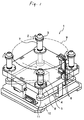
- Figs. 1 and 2 are a perspective view and a side view of a preferred embodiment of an aligner apparatus of the present invention.
- a plate 8 is fixed to a pedestal 10 through a leg portion 10' (in Fig. 1, one at this side is shown).
- This pedestal 10 is for only setting the plate 8, a relevant control apparatus, and the like, and becomes unnecessary when the aligner apparatus is directly installed in a semiconductor manufacturing apparatus.
- spindles 7 are axially supported at approximately four corners of the plate 8. As described below, the spindles 7 are located at positions where they can support a circular semiconductor substrate 9. As is well shown in Fig. 2, the spindle 7 is attached to the plate 8 through a bearing 14 provided in a hole bored in the plate 8.
- a nut 12 is attached to a lower portion of the spindle 7 protruding from the hole of the plate 8, and a cover 15 is attached to its upper portion. In this way, the spindle 7 is rotatably axially supported by the plate 8.
- Holding means is provided at a tip end of each of the spindles 7.
- This holding means includes a guide portion 2 of a spherical or taper shape, and a roller 3 continued from this and having a taper-shaped shoulder portion 13.
- the semiconductor substrate 9 is held, while its edge portion is brought into contact with the taper-shaped shoulder portion 13 of the roller 3 of the holding means provided on each of the spindles 7.
- the semiconductor substrate 9 is conveyed to the shoulder portion 13 by conveying means (not shown), even if a little position error exists at that time, it is guided to the shoulder portion 13 along the sloped side of the guide portion 2.
- the guide portion is provided for this, if the conveying means can dispose the semiconductor substrate 9 to each of the shoulder portions 13 of the rollers, the guide portion becomes unnecessary.
- the semiconductor substrate 9 when the semiconductor substrate 9 is disposed to each of the should portions 13 of the rollers 3 of the holding means, and the spindles 7 are rotated to rotate the rollers 3 of the holding means, interlocking with the rotation, the semiconductor substrate 9 being in contact with and supported by the should portions 13 can also be rotated around the axial line.
- roller 3 comes in contact with the edge portion of the semiconductor substrate 9, and transmits the rotation of the roller 3 to the semiconductor substrate 9, it is desirable that a rubber lining is provided in order to reduce damage at the contact and to prevent a slip between both during the rotation.
- the holding means is for holding and rotating the semiconductor substrate 9, at least three holding means are sufficient (the number of the spindles to which they are attached is also the same).
- the edge portion of the semiconductor substrate 9 comes in contact with the roller 3 of each of the holding means.
- the number is four or more, there is a case where some roller 3 does not come in contact with the edge portion of the semiconductor substrate. In such a case, it becomes hard to transmit the rotation of the spindle to the semiconductor substrate through the holding means, and the rotation of the semiconductor substrate becomes unstable.
- a floating mechanism is provided for at least one holding member.
- a hollow cylindrical portion 32 capable of housing the upper portion of the spindle 7 extends downward from a roller 31 of holding means 30 including this floating mechanism.
- a hole 34 capable of housing a spring 33 is formed in the inside of a tip end of the spindle 7.
- the spring 33 performs an action to push up the holding means 30 when the holding means 30 is pushed down.
- a groove 35 is formed along an axial line on the side of the cylindrical portion 32 so that although the cylindrical portion 32 can move in the axial direction with respect to the spindle 7, they can not rotate relatively to each other, and a guide pin 36 passing through the groove 35 and preventing the relative rotation is fixed to the spindle 7.
- the holding means protrudes upward from other holding means.
- the conveyed semiconductor substrate first comes in contact with the roller of the holding means having the floating mechanism.
- the roller goes down by the weight of the semiconductor substrate until the edge portion of the semiconductor substrate comes in contact with the roller of other holding means, the roller continues to be in contact with the edge portion of the semiconductor substrate by the repulsive force of the spring 33, and therefore, all rollers can come in contact with the edge portion of the semiconductor substrate.
- a pulley 11 is attached to a lower end of each of the spindles 7.
- a timing belt 5 is hung on the pulley 11.
- the timing belt 5 is hung also on a pulse motor 4 fixed to the rear surface of the plate 8.
- the pulse motor 4 is started, the four spindles are rotated through the timing belt 5.
- the rotation of the pulse motor 4 is transmitted in synchronization with the respective spindles.
- the rotation of the pulse motor 4 may also be transmitted to the spindles by using a gear instead of the timing belt.
- the four spindles are rotated by using the timing belt, by rotating one spindle (in this case, the timing belt becomes unnecessary), it is also possible to rotate the semiconductor substrate positioned thereon. However, for more certain rotation, it is desirable that two spindles positioned diagonally are rotated (in this case, a timing belt is hung on the spindles to be rotated).
- a sensor 6 is set above and below the edge portion of the semiconductor substrate 9. A part of light emitted from the upper element of the sensor is blocked off by the semiconductor substrate (in Fig. 1, indicated by a plane depicted by a one-dot-chain line).
- the semiconductor substrate rotates and when the notch or "orifla” passes through the place of the sensor 6, the amount of blocked light is changed, and this is detected by the lower element. In this way, the position of the notch or "orifla” of the semiconductor substrate is detected by the sensor.
- the sensor 6 After detecting the notch or "orifla" of the semiconductor substrate 9, the sensor 6 transmits a signal to the pulse motor 4, and the pulse motor 4 makes a predetermined number of rotations through pulse control.
- the rotation is transmitted to the spindle 7 through the timing belt, the roller of the holding means attached to the spindle is rotated, and the semiconductor substrate 9 is interlocked with the roller 3 and is rotated until the notch or "orifla" reaches a predetermined position.
- the one sensor 6 is provided in this embodiment, a plurality of sensors may be provided.
- the semiconductor substrate 9 is conveyed by conveying means (not shown) to the upper vicinity of the holding means.
- the conveying means slowly falls vertically downward, and the semiconductor substrate 9 is inserted between the guide portions 2.
- the guide portion 2 guides the semiconductor substrate 9 to the taper-shaped shoulder portion 13 of the roller 3. Even if a position shift slightly occurs when the semiconductor substrate is inserted between the guide portions, the semiconductor substrate is guided by the guide portion and is put on the roller. This means that centering of the semiconductor substrate is also performed.
- the four spindles 7 are synchronously rotated through the timing belt 5.
- the holding means provided to the spindle is also rotated, and interlocking with the rotation, the semiconductor substrate 9 thereon rotates around the axial line.
- the notch or "orifla” of the semiconductor substrate 9 passes through the place of the sensor 6, the sensor 6 detects that. Then, a signal for causing a certain number of rotations necessary for the notch or "orifla” to reach the predetermined position is transmitted to the pulse motor 4.
- the conveying means may stand by at a lower side of the semiconductor substrate 9, while the semiconductor substrate 9 is interlocked with the rotation of the holding means and is rotated.
- the notch or "orifla" reaches the predetermined position, and alignment of the semiconductor substrate is completed.
- the conveying means goes up, and can move the semiconductor substrate 9 to a next processing step while supporting the aligned and centered semiconductor substrate 9.
Landscapes
- Container, Conveyance, Adherence, Positioning, Of Wafer (AREA)
- Registering Or Overturning Sheets (AREA)
Applications Claiming Priority (4)
| Application Number | Priority Date | Filing Date | Title |
|---|---|---|---|
| JP19508799 | 1999-07-08 | ||
| JP19508799 | 1999-07-08 | ||
| JP21734899 | 1999-07-30 | ||
| JP21734899A JP3245833B2 (ja) | 1999-07-08 | 1999-07-30 | 半導体基板アライナー装置および方法 |
Publications (2)
| Publication Number | Publication Date |
|---|---|
| EP1067589A2 true EP1067589A2 (de) | 2001-01-10 |
| EP1067589A3 EP1067589A3 (de) | 2006-07-12 |
Family
ID=26508916
Family Applications (1)
| Application Number | Title | Priority Date | Filing Date |
|---|---|---|---|
| EP00202403A Ceased EP1067589A3 (de) | 1999-07-08 | 2000-07-06 | Vorrichtung und Verfahren zur Ausrichtung von einem Halbleitersubstrat |
Country Status (5)
| Country | Link |
|---|---|
| US (1) | US6454516B1 (de) |
| EP (1) | EP1067589A3 (de) |
| JP (1) | JP3245833B2 (de) |
| KR (1) | KR20010039706A (de) |
| TW (1) | TW478088B (de) |
Cited By (7)
| Publication number | Priority date | Publication date | Assignee | Title |
|---|---|---|---|---|
| EP1450392A1 (de) * | 2003-02-20 | 2004-08-25 | Applied Materials, Inc. | Eine Methode und eine Vorrichtung um ein Substrat relativ zu einer Halterung zu positionieren |
| US7104535B2 (en) | 2003-02-20 | 2006-09-12 | Applied Materials, Inc. | Methods and apparatus for positioning a substrate relative to a support stage |
| US7151981B2 (en) | 2003-02-20 | 2006-12-19 | Applied Materials, Inc. | Methods and apparatus for positioning a substrate relative to a support stage |
| US7372250B2 (en) | 2003-02-20 | 2008-05-13 | Applied Materials, Inc. | Methods and apparatus for determining a position of a substrate relative to a support stage |
| US7499767B2 (en) | 2003-02-20 | 2009-03-03 | Applied Materials, Inc. | Methods and apparatus for positioning a substrate relative to a support stage |
| US7625063B2 (en) | 2004-11-04 | 2009-12-01 | Applied Materials, Inc. | Apparatus and methods for an inkjet head support having an inkjet head capable of independent lateral movement |
| WO2013102351A1 (zh) * | 2012-01-05 | 2013-07-11 | 沈阳新松机器人自动化股份有限公司 | 透光夹持式预对准机 |
Families Citing this family (18)
| Publication number | Priority date | Publication date | Assignee | Title |
|---|---|---|---|---|
| DE10121010B4 (de) * | 2001-04-28 | 2007-06-28 | Infineon Technologies Ag | Halter für Halbleiterwafer in einer Bürstenreinigungsanlage |
| KR20030021653A (ko) * | 2001-09-07 | 2003-03-15 | 삼성전자주식회사 | 웨이퍼 스테이지 및 이를 이용한 베이크 장치 |
| US7256132B2 (en) * | 2002-07-31 | 2007-08-14 | Applied Materials, Inc. | Substrate centering apparatus and method |
| KR100814448B1 (ko) * | 2003-12-12 | 2008-03-17 | 한미반도체 주식회사 | 반도체 패키지 건조시스템 |
| JP4467367B2 (ja) * | 2004-06-22 | 2010-05-26 | 大日本スクリーン製造株式会社 | 基板反転装置、基板搬送装置、基板処理装置、基板反転方法、基板搬送方法および基板処理方法 |
| JP4410063B2 (ja) * | 2004-09-06 | 2010-02-03 | 東京エレクトロン株式会社 | 基板処理装置 |
| US9202725B2 (en) * | 2006-07-24 | 2015-12-01 | Planar Semiconductor, Inc. | Holding and rotary driving mechanism for flat objects |
| KR100872267B1 (ko) * | 2007-07-23 | 2008-12-05 | 주식회사 윌비에스엔티 | 웨이퍼 토글 롤러 결합구조 |
| JP5723612B2 (ja) * | 2011-01-28 | 2015-05-27 | リンテック株式会社 | 板状部材の支持装置 |
| CN103206591B (zh) * | 2012-01-11 | 2016-10-05 | 昆山允升吉光电科技有限公司 | 电动载物台定位方法 |
| CN103985662B (zh) * | 2014-04-24 | 2017-07-04 | 京东方科技集团股份有限公司 | 一种对位装置及对位平台 |
| TWM549447U (zh) * | 2016-11-23 | 2017-09-21 | 辛耘企業股份有限公司 | 基板對準及檢測裝置與基板處理機台 |
| CN110729216A (zh) * | 2019-10-21 | 2020-01-24 | 华虹半导体(无锡)有限公司 | 晶圆位置检测装置、晶圆位置检测方法 |
| KR102308346B1 (ko) * | 2021-01-12 | 2021-10-01 | (주)볼타오토메이션 | 웨이퍼의 센터링 장치 |
| CN112967995B (zh) * | 2021-02-01 | 2022-12-30 | 泉芯集成电路制造(济南)有限公司 | 一种芯片夹具、芯片清洗装置及芯片刻蚀装置 |
| WO2024233209A1 (en) * | 2023-05-10 | 2024-11-14 | Jabil Inc. | Apparatus, system and method for aligning flat panels and film frames |
| TWD231773S (zh) * | 2023-07-13 | 2024-06-11 | 韓商維比S&T股份有限公司 (南韓) | 晶圓撥動滾輪 |
| TWD233403S (zh) * | 2023-07-13 | 2024-09-01 | 韓商維比S&T股份有限公司 (南韓) | 晶圓撥動滾輪 |
Family Cites Families (31)
| Publication number | Priority date | Publication date | Assignee | Title |
|---|---|---|---|---|
| US2957252A (en) * | 1959-12-11 | 1960-10-25 | William A Pain | Globe support and orienting means |
| US3389778A (en) * | 1967-04-20 | 1968-06-25 | Heisler Company | Apparatus for orienting eared containers |
| US3972424A (en) * | 1973-03-12 | 1976-08-03 | The Computervision Corporation | Automatic wafer loading and pre-alignment system |
| JPS50122879A (de) * | 1974-03-13 | 1975-09-26 | ||
| US4242038A (en) * | 1979-06-29 | 1980-12-30 | International Business Machines Corporation | Wafer orienting apparatus |
| JPS5666036A (en) * | 1979-11-05 | 1981-06-04 | Canon Inc | Wafer positioner |
| US4377038A (en) * | 1981-02-19 | 1983-03-22 | Fmc Corporation | Truck wheel clamp with floating spindle plate |
| JPH0610775B2 (ja) * | 1984-12-05 | 1994-02-09 | 株式会社ニコン | 円形基板の位置決め装置 |
| US4887904A (en) * | 1985-08-23 | 1989-12-19 | Canon Kabushiki Kaisha | Device for positioning a semi-conductor wafer |
| JPS6386447A (ja) * | 1986-09-30 | 1988-04-16 | Nippon Seiko Kk | 露光装置用被露光部材位置決め装置 |
| US5085558A (en) * | 1987-02-09 | 1992-02-04 | Svg Lithography Systems, Inc. | Wafer handling system |
| EP0350752B1 (de) * | 1988-07-15 | 1993-10-13 | Balzers Aktiengesellschaft | Haltevorrichtung für eine Scheibe sowie Anwendung derselben |
| US5052886A (en) * | 1988-12-20 | 1991-10-01 | Texas Instruments Incorporated | Semiconductor wafer orientation device |
| EP0416727A3 (en) | 1989-07-18 | 1992-03-25 | Petrus Joubert Van Der Walt | Method and apparatus for providing stereoscopic images |
| JP3180357B2 (ja) * | 1990-04-06 | 2001-06-25 | 株式会社ニコン | 円形基板の位置決め装置および方法 |
| US5385186A (en) * | 1993-11-12 | 1995-01-31 | Forest Products Machinery, Inc. | Sharp chain charger |
| US5566466A (en) * | 1994-07-01 | 1996-10-22 | Ontrak Systems, Inc. | Spindle assembly with improved wafer holder |
| US6003185A (en) * | 1994-07-15 | 1999-12-21 | Ontrak Systems, Inc. | Hesitation free roller |
| US5551829A (en) * | 1995-10-11 | 1996-09-03 | H-Square Corporation | Notch finder having a flexible alignment rod |
| JPH09246357A (ja) * | 1996-03-04 | 1997-09-19 | Zetetsuku Kk | 半導体ウエハの一斉方向合わせ方法及びその装置 |
| US5851041A (en) * | 1996-06-26 | 1998-12-22 | Ontrak Systems, Inc. | Wafer holder with spindle assembly and wafer holder actuator |
| US5662452A (en) * | 1996-08-26 | 1997-09-02 | H-Square Corporation | Apparatus and method of aligning notches using a free-floating rod |
| US5853284A (en) * | 1996-09-24 | 1998-12-29 | Kaijo Corporation | Notched wafer aligning apparatus |
| US5880479A (en) * | 1996-10-25 | 1999-03-09 | Vanguard International Semiconductor Corporation | Wafer aligner apparatus using different diameter rollers |
| WO1999041022A1 (en) * | 1998-02-14 | 1999-08-19 | Strasbaugh | Accurate positioning of a wafer |
| KR100343153B1 (ko) | 1998-03-30 | 2002-09-18 | 삼성전자 주식회사 | 광기록재생장치 |
| TW412817B (en) * | 1998-06-19 | 2000-11-21 | Matsushita Electric Industrial Co Ltd | A bump bonding apparatus and method |
| FR2780961B1 (fr) * | 1998-07-10 | 2000-10-13 | Dubuit Mach | Dispositifs de chargement et dechargement pour machine d'impression |
| US6270307B1 (en) * | 1999-01-25 | 2001-08-07 | Chartered Semiconductor Manufacturing Company | Method for aligning wafers in a cassette |
| US6357996B2 (en) * | 1999-05-14 | 2002-03-19 | Newport Corporation | Edge gripping specimen prealigner |
| JP3116039U (ja) | 2005-08-23 | 2005-11-24 | 岡本株式会社 | 靴下 |
-
1999
- 1999-07-30 JP JP21734899A patent/JP3245833B2/ja not_active Expired - Fee Related
-
2000
- 2000-06-23 TW TW089112463A patent/TW478088B/zh not_active IP Right Cessation
- 2000-07-06 EP EP00202403A patent/EP1067589A3/de not_active Ceased
- 2000-07-07 KR KR1020000038769A patent/KR20010039706A/ko not_active Ceased
- 2000-07-10 US US09/612,739 patent/US6454516B1/en not_active Expired - Fee Related
Cited By (9)
| Publication number | Priority date | Publication date | Assignee | Title |
|---|---|---|---|---|
| EP1450392A1 (de) * | 2003-02-20 | 2004-08-25 | Applied Materials, Inc. | Eine Methode und eine Vorrichtung um ein Substrat relativ zu einer Halterung zu positionieren |
| KR100587781B1 (ko) * | 2003-02-20 | 2006-06-09 | 어플라이드 머티어리얼스, 인코포레이티드 | 지지 스테이지에 대한 기판의 위치결정 장치 및 방법 |
| US7104535B2 (en) | 2003-02-20 | 2006-09-12 | Applied Materials, Inc. | Methods and apparatus for positioning a substrate relative to a support stage |
| US7151981B2 (en) | 2003-02-20 | 2006-12-19 | Applied Materials, Inc. | Methods and apparatus for positioning a substrate relative to a support stage |
| US7372250B2 (en) | 2003-02-20 | 2008-05-13 | Applied Materials, Inc. | Methods and apparatus for determining a position of a substrate relative to a support stage |
| CN100399534C (zh) * | 2003-02-20 | 2008-07-02 | 应用材料有限公司 | 相对于支撑台定位基片的方法与设备 |
| US7499767B2 (en) | 2003-02-20 | 2009-03-03 | Applied Materials, Inc. | Methods and apparatus for positioning a substrate relative to a support stage |
| US7625063B2 (en) | 2004-11-04 | 2009-12-01 | Applied Materials, Inc. | Apparatus and methods for an inkjet head support having an inkjet head capable of independent lateral movement |
| WO2013102351A1 (zh) * | 2012-01-05 | 2013-07-11 | 沈阳新松机器人自动化股份有限公司 | 透光夹持式预对准机 |
Also Published As
| Publication number | Publication date |
|---|---|
| US6454516B1 (en) | 2002-09-24 |
| KR20010039706A (ko) | 2001-05-15 |
| JP2001077179A (ja) | 2001-03-23 |
| JP3245833B2 (ja) | 2002-01-15 |
| TW478088B (en) | 2002-03-01 |
| EP1067589A3 (de) | 2006-07-12 |
Similar Documents
| Publication | Publication Date | Title |
|---|---|---|
| EP1067589A2 (de) | Vorrichtung und Verfahren zur Ausrichtung von einem Halbleitersubstrat | |
| US5940960A (en) | Automatic valve stemming method and apparatus | |
| US4483434A (en) | Apparatus for conveying semiconductor substrates | |
| US20010043858A1 (en) | Edge gripping specimen prealigner | |
| CN111029291A (zh) | 一种晶圆定位装置及具有其的减薄机 | |
| JP2002289673A (ja) | 搬出入装置 | |
| JP7786301B2 (ja) | 円筒研削機 | |
| US20040004713A1 (en) | Method of and apparatus for detecting a defect at the outer peripheral edge of a wafer, and cleaning equipment comprising the apparatus | |
| CN117276167A (zh) | 一种晶圆上料平边自动对齐装置及晶圆生产线 | |
| US5139132A (en) | Orientation apparatus and method for disk shaped parts | |
| US6682295B2 (en) | Flatted object passive aligner | |
| EP0911114B1 (de) | Poliervorrichtung | |
| KR980012221A (ko) | 웨이퍼의 자동 정렬장치 | |
| KR100743466B1 (ko) | 기판 이송 장치용 기판 감지 장치 | |
| KR100625280B1 (ko) | 후프 오프너의 후프이송장치 | |
| US20020034434A1 (en) | Wafer flat zone aligner | |
| US20020075478A1 (en) | Inspection device having wafer exchange stage | |
| JP2000146849A (ja) | 円筒体の自動外観検査装置 | |
| JP2002043393A (ja) | ノッチ合わせ装置 | |
| KR20070003396A (ko) | 웨이퍼 이송 장치 | |
| KR20110105572A (ko) | 반도체 웨이퍼 반송용 핸드 | |
| JP3478682B2 (ja) | ノッチ付きウェーハ整列装置 | |
| JP3704365B2 (ja) | ウエハ検査装置 | |
| JPH08255821A (ja) | シリコンウェハー搬送装置 | |
| JP2002319559A (ja) | 研削装置 |
Legal Events
| Date | Code | Title | Description |
|---|---|---|---|
| PUAI | Public reference made under article 153(3) epc to a published international application that has entered the european phase |
Free format text: ORIGINAL CODE: 0009012 |
|
| AK | Designated contracting states |
Kind code of ref document: A2 Designated state(s): AT BE CH CY DE DK ES FI FR GB GR IE IT LI LU MC NL PT SE |
|
| AX | Request for extension of the european patent |
Free format text: AL;LT;LV;MK;RO;SI |
|
| PUAL | Search report despatched |
Free format text: ORIGINAL CODE: 0009013 |
|
| AK | Designated contracting states |
Kind code of ref document: A3 Designated state(s): AT BE CH CY DE DK ES FI FR GB GR IE IT LI LU MC NL PT SE |
|
| AX | Request for extension of the european patent |
Extension state: AL LT LV MK RO SI |
|
| 17P | Request for examination filed |
Effective date: 20070111 |
|
| AKX | Designation fees paid |
Designated state(s): DE |
|
| 17Q | First examination report despatched |
Effective date: 20070319 |
|
| STAA | Information on the status of an ep patent application or granted ep patent |
Free format text: STATUS: THE APPLICATION HAS BEEN REFUSED |
|
| 18R | Application refused |
Effective date: 20071207 |