EP1073106A2 - Verfahren zur Verringerung der Oxidation an einer Zwischenschicht einer Halbleiteranordnung, und resultierende Anordnung - Google Patents
Verfahren zur Verringerung der Oxidation an einer Zwischenschicht einer Halbleiteranordnung, und resultierende Anordnung Download PDFInfo
- Publication number
- EP1073106A2 EP1073106A2 EP00109718A EP00109718A EP1073106A2 EP 1073106 A2 EP1073106 A2 EP 1073106A2 EP 00109718 A EP00109718 A EP 00109718A EP 00109718 A EP00109718 A EP 00109718A EP 1073106 A2 EP1073106 A2 EP 1073106A2
- Authority
- EP
- European Patent Office
- Prior art keywords
- interface
- layer
- plasma
- insulating layer
- semiconductor device
- Prior art date
- Legal status (The legal status is an assumption and is not a legal conclusion. Google has not performed a legal analysis and makes no representation as to the accuracy of the status listed.)
- Granted
Links
Images

Classifications
-
- H—ELECTRICITY
- H10—SEMICONDUCTOR DEVICES; ELECTRIC SOLID-STATE DEVICES NOT OTHERWISE PROVIDED FOR
- H10P—GENERIC PROCESSES OR APPARATUS FOR THE MANUFACTURE OR TREATMENT OF DEVICES COVERED BY CLASS H10
- H10P14/00—Formation of materials, e.g. in the shape of layers or pillars
- H10P14/60—Formation of materials, e.g. in the shape of layers or pillars of insulating materials
- H10P14/63—Formation of materials, e.g. in the shape of layers or pillars of insulating materials characterised by the formation processes
- H10P14/6326—Deposition processes
- H10P14/6328—Deposition from the gas or vapour phase
- H10P14/6334—Deposition from the gas or vapour phase using decomposition or reaction of gaseous or vapour phase compounds, i.e. chemical vapour deposition
- H10P14/6336—Deposition from the gas or vapour phase using decomposition or reaction of gaseous or vapour phase compounds, i.e. chemical vapour deposition in the presence of a plasma [PECVD]
-
- H—ELECTRICITY
- H10—SEMICONDUCTOR DEVICES; ELECTRIC SOLID-STATE DEVICES NOT OTHERWISE PROVIDED FOR
- H10P—GENERIC PROCESSES OR APPARATUS FOR THE MANUFACTURE OR TREATMENT OF DEVICES COVERED BY CLASS H10
- H10P14/00—Formation of materials, e.g. in the shape of layers or pillars
- H10P14/60—Formation of materials, e.g. in the shape of layers or pillars of insulating materials
-
- B—PERFORMING OPERATIONS; TRANSPORTING
- B08—CLEANING
- B08B—CLEANING IN GENERAL; PREVENTION OF FOULING IN GENERAL
- B08B7/00—Cleaning by methods not provided for in a single other subclass or a single group in this subclass
- B08B7/0035—Cleaning by methods not provided for in a single other subclass or a single group in this subclass by radiant energy, e.g. UV, laser, light beam or the like
-
- C—CHEMISTRY; METALLURGY
- C23—COATING METALLIC MATERIAL; COATING MATERIAL WITH METALLIC MATERIAL; CHEMICAL SURFACE TREATMENT; DIFFUSION TREATMENT OF METALLIC MATERIAL; COATING BY VACUUM EVAPORATION, BY SPUTTERING, BY ION IMPLANTATION OR BY CHEMICAL VAPOUR DEPOSITION, IN GENERAL; INHIBITING CORROSION OF METALLIC MATERIAL OR INCRUSTATION IN GENERAL
- C23C—COATING METALLIC MATERIAL; COATING MATERIAL WITH METALLIC MATERIAL; SURFACE TREATMENT OF METALLIC MATERIAL BY DIFFUSION INTO THE SURFACE, BY CHEMICAL CONVERSION OR SUBSTITUTION; COATING BY VACUUM EVAPORATION, BY SPUTTERING, BY ION IMPLANTATION OR BY CHEMICAL VAPOUR DEPOSITION, IN GENERAL
- C23C16/00—Chemical coating by decomposition of gaseous compounds, without leaving reaction products of surface material in the coating, i.e. chemical vapour deposition [CVD] processes
- C23C16/02—Pretreatment of the material to be coated
- C23C16/0227—Pretreatment of the material to be coated by cleaning or etching
- C23C16/0245—Pretreatment of the material to be coated by cleaning or etching by etching with a plasma
-
- C—CHEMISTRY; METALLURGY
- C23—COATING METALLIC MATERIAL; COATING MATERIAL WITH METALLIC MATERIAL; CHEMICAL SURFACE TREATMENT; DIFFUSION TREATMENT OF METALLIC MATERIAL; COATING BY VACUUM EVAPORATION, BY SPUTTERING, BY ION IMPLANTATION OR BY CHEMICAL VAPOUR DEPOSITION, IN GENERAL; INHIBITING CORROSION OF METALLIC MATERIAL OR INCRUSTATION IN GENERAL
- C23G—CLEANING OR DE-GREASING OF METALLIC MATERIAL BY CHEMICAL METHODS OTHER THAN ELECTROLYSIS
- C23G5/00—Cleaning or de-greasing metallic material by other methods; Apparatus for cleaning or de-greasing metallic material with organic solvents
-
- H—ELECTRICITY
- H10—SEMICONDUCTOR DEVICES; ELECTRIC SOLID-STATE DEVICES NOT OTHERWISE PROVIDED FOR
- H10P—GENERIC PROCESSES OR APPARATUS FOR THE MANUFACTURE OR TREATMENT OF DEVICES COVERED BY CLASS H10
- H10P14/00—Formation of materials, e.g. in the shape of layers or pillars
- H10P14/60—Formation of materials, e.g. in the shape of layers or pillars of insulating materials
- H10P14/65—Formation of materials, e.g. in the shape of layers or pillars of insulating materials characterised by treatments performed before or after the formation of the materials
- H10P14/6516—Formation of materials, e.g. in the shape of layers or pillars of insulating materials characterised by treatments performed before or after the formation of the materials of treatments performed after formation of the materials
- H10P14/6529—Formation of materials, e.g. in the shape of layers or pillars of insulating materials characterised by treatments performed before or after the formation of the materials of treatments performed after formation of the materials by exposure to a gas or vapour
- H10P14/6532—Formation of materials, e.g. in the shape of layers or pillars of insulating materials characterised by treatments performed before or after the formation of the materials of treatments performed after formation of the materials by exposure to a gas or vapour by exposure to a plasma
-
- H—ELECTRICITY
- H10—SEMICONDUCTOR DEVICES; ELECTRIC SOLID-STATE DEVICES NOT OTHERWISE PROVIDED FOR
- H10P—GENERIC PROCESSES OR APPARATUS FOR THE MANUFACTURE OR TREATMENT OF DEVICES COVERED BY CLASS H10
- H10P14/00—Formation of materials, e.g. in the shape of layers or pillars
- H10P14/60—Formation of materials, e.g. in the shape of layers or pillars of insulating materials
- H10P14/66—Formation of materials, e.g. in the shape of layers or pillars of insulating materials characterised by the type of materials
- H10P14/668—Formation of materials, e.g. in the shape of layers or pillars of insulating materials characterised by the type of materials the materials being characterised by the deposition precursor materials
- H10P14/6681—Formation of materials, e.g. in the shape of layers or pillars of insulating materials characterised by the type of materials the materials being characterised by the deposition precursor materials the precursor containing a compound comprising Si
- H10P14/6682—Formation of materials, e.g. in the shape of layers or pillars of insulating materials characterised by the type of materials the materials being characterised by the deposition precursor materials the precursor containing a compound comprising Si the compound being a silane, e.g. disilane, methylsilane or chlorosilane
-
- H—ELECTRICITY
- H10—SEMICONDUCTOR DEVICES; ELECTRIC SOLID-STATE DEVICES NOT OTHERWISE PROVIDED FOR
- H10P—GENERIC PROCESSES OR APPARATUS FOR THE MANUFACTURE OR TREATMENT OF DEVICES COVERED BY CLASS H10
- H10P14/00—Formation of materials, e.g. in the shape of layers or pillars
- H10P14/60—Formation of materials, e.g. in the shape of layers or pillars of insulating materials
- H10P14/69—Inorganic materials
- H10P14/694—Inorganic materials composed of nitrides
- H10P14/6943—Inorganic materials composed of nitrides containing silicon
- H10P14/69433—Inorganic materials composed of nitrides containing silicon the material being a silicon nitride not containing oxygen, e.g. SixNy or SixByNz
-
- H—ELECTRICITY
- H10—SEMICONDUCTOR DEVICES; ELECTRIC SOLID-STATE DEVICES NOT OTHERWISE PROVIDED FOR
- H10P—GENERIC PROCESSES OR APPARATUS FOR THE MANUFACTURE OR TREATMENT OF DEVICES COVERED BY CLASS H10
- H10P50/00—Etching of wafers, substrates or parts of devices
- H10P50/20—Dry etching; Plasma etching; Reactive-ion etching
- H10P50/26—Dry etching; Plasma etching; Reactive-ion etching of conductive or resistive materials
- H10P50/264—Dry etching; Plasma etching; Reactive-ion etching of conductive or resistive materials by chemical means
- H10P50/266—Dry etching; Plasma etching; Reactive-ion etching of conductive or resistive materials by chemical means by vapour etching only
- H10P50/267—Dry etching; Plasma etching; Reactive-ion etching of conductive or resistive materials by chemical means by vapour etching only using plasmas
-
- H—ELECTRICITY
- H10—SEMICONDUCTOR DEVICES; ELECTRIC SOLID-STATE DEVICES NOT OTHERWISE PROVIDED FOR
- H10P—GENERIC PROCESSES OR APPARATUS FOR THE MANUFACTURE OR TREATMENT OF DEVICES COVERED BY CLASS H10
- H10P50/00—Etching of wafers, substrates or parts of devices
- H10P50/20—Dry etching; Plasma etching; Reactive-ion etching
- H10P50/28—Dry etching; Plasma etching; Reactive-ion etching of insulating materials
- H10P50/282—Dry etching; Plasma etching; Reactive-ion etching of insulating materials of inorganic materials
- H10P50/283—Dry etching; Plasma etching; Reactive-ion etching of insulating materials of inorganic materials by chemical means
-
- H—ELECTRICITY
- H10—SEMICONDUCTOR DEVICES; ELECTRIC SOLID-STATE DEVICES NOT OTHERWISE PROVIDED FOR
- H10P—GENERIC PROCESSES OR APPARATUS FOR THE MANUFACTURE OR TREATMENT OF DEVICES COVERED BY CLASS H10
- H10P70/00—Cleaning of wafers, substrates or parts of devices
- H10P70/20—Cleaning during device manufacture
- H10P70/23—Cleaning during device manufacture during, before or after processing of insulating materials
- H10P70/234—Cleaning during device manufacture during, before or after processing of insulating materials the processing being the formation of vias or contact holes
-
- H—ELECTRICITY
- H10—SEMICONDUCTOR DEVICES; ELECTRIC SOLID-STATE DEVICES NOT OTHERWISE PROVIDED FOR
- H10P—GENERIC PROCESSES OR APPARATUS FOR THE MANUFACTURE OR TREATMENT OF DEVICES COVERED BY CLASS H10
- H10P70/00—Cleaning of wafers, substrates or parts of devices
- H10P70/20—Cleaning during device manufacture
- H10P70/27—Cleaning during device manufacture during, before or after processing of conductive materials, e.g. polysilicon or amorphous silicon layers
-
- H—ELECTRICITY
- H10—SEMICONDUCTOR DEVICES; ELECTRIC SOLID-STATE DEVICES NOT OTHERWISE PROVIDED FOR
- H10P—GENERIC PROCESSES OR APPARATUS FOR THE MANUFACTURE OR TREATMENT OF DEVICES COVERED BY CLASS H10
- H10P70/00—Cleaning of wafers, substrates or parts of devices
- H10P70/20—Cleaning during device manufacture
- H10P70/27—Cleaning during device manufacture during, before or after processing of conductive materials, e.g. polysilicon or amorphous silicon layers
- H10P70/277—Cleaning during device manufacture during, before or after processing of conductive materials, e.g. polysilicon or amorphous silicon layers the processing being a planarisation of conductive layers
-
- H—ELECTRICITY
- H10—SEMICONDUCTOR DEVICES; ELECTRIC SOLID-STATE DEVICES NOT OTHERWISE PROVIDED FOR
- H10W—GENERIC PACKAGES, INTERCONNECTIONS, CONNECTORS OR OTHER CONSTRUCTIONAL DETAILS OF DEVICES COVERED BY CLASS H10
- H10W20/00—Interconnections in chips, wafers or substrates
- H10W20/01—Manufacture or treatment
- H10W20/031—Manufacture or treatment of conductive parts of the interconnections
- H10W20/056—Manufacture or treatment of conductive parts of the interconnections by filling conductive material into holes, grooves or trenches
-
- H—ELECTRICITY
- H10—SEMICONDUCTOR DEVICES; ELECTRIC SOLID-STATE DEVICES NOT OTHERWISE PROVIDED FOR
- H10W—GENERIC PACKAGES, INTERCONNECTIONS, CONNECTORS OR OTHER CONSTRUCTIONAL DETAILS OF DEVICES COVERED BY CLASS H10
- H10W20/00—Interconnections in chips, wafers or substrates
- H10W20/01—Manufacture or treatment
- H10W20/071—Manufacture or treatment of dielectric parts thereof
- H10W20/074—Manufacture or treatment of dielectric parts thereof of dielectric parts comprising thin functional dielectric layers, e.g. dielectric etch-stop, barrier, capping or liner layers
- H10W20/077—Manufacture or treatment of dielectric parts thereof of dielectric parts comprising thin functional dielectric layers, e.g. dielectric etch-stop, barrier, capping or liner layers on sidewalls or on top surfaces of conductors
-
- H—ELECTRICITY
- H10—SEMICONDUCTOR DEVICES; ELECTRIC SOLID-STATE DEVICES NOT OTHERWISE PROVIDED FOR
- H10W—GENERIC PACKAGES, INTERCONNECTIONS, CONNECTORS OR OTHER CONSTRUCTIONAL DETAILS OF DEVICES COVERED BY CLASS H10
- H10W20/00—Interconnections in chips, wafers or substrates
- H10W20/40—Interconnections external to wafers or substrates, e.g. back-end-of-line [BEOL] metallisations or vias connecting to gate electrodes
- H10W20/41—Interconnections external to wafers or substrates, e.g. back-end-of-line [BEOL] metallisations or vias connecting to gate electrodes characterised by their conductive parts
- H10W20/425—Barrier, adhesion or liner layers
-
- H—ELECTRICITY
- H10—SEMICONDUCTOR DEVICES; ELECTRIC SOLID-STATE DEVICES NOT OTHERWISE PROVIDED FOR
- H10P—GENERIC PROCESSES OR APPARATUS FOR THE MANUFACTURE OR TREATMENT OF DEVICES COVERED BY CLASS H10
- H10P14/00—Formation of materials, e.g. in the shape of layers or pillars
- H10P14/60—Formation of materials, e.g. in the shape of layers or pillars of insulating materials
- H10P14/69—Inorganic materials
- H10P14/6902—Inorganic materials composed of carbon, e.g. alpha-C, diamond or hydrogen doped carbon
-
- H—ELECTRICITY
- H10—SEMICONDUCTOR DEVICES; ELECTRIC SOLID-STATE DEVICES NOT OTHERWISE PROVIDED FOR
- H10P—GENERIC PROCESSES OR APPARATUS FOR THE MANUFACTURE OR TREATMENT OF DEVICES COVERED BY CLASS H10
- H10P14/00—Formation of materials, e.g. in the shape of layers or pillars
- H10P14/60—Formation of materials, e.g. in the shape of layers or pillars of insulating materials
- H10P14/69—Inorganic materials
- H10P14/6903—Inorganic materials containing silicon
- H10P14/6905—Inorganic materials containing silicon being a silicon carbide or silicon carbonitride and not containing oxygen, e.g. SiC or SiC:H
-
- H—ELECTRICITY
- H10—SEMICONDUCTOR DEVICES; ELECTRIC SOLID-STATE DEVICES NOT OTHERWISE PROVIDED FOR
- H10P—GENERIC PROCESSES OR APPARATUS FOR THE MANUFACTURE OR TREATMENT OF DEVICES COVERED BY CLASS H10
- H10P14/00—Formation of materials, e.g. in the shape of layers or pillars
- H10P14/60—Formation of materials, e.g. in the shape of layers or pillars of insulating materials
- H10P14/69—Inorganic materials
- H10P14/692—Inorganic materials composed of oxides, glassy oxides or oxide-based glasses
- H10P14/6921—Inorganic materials composed of oxides, glassy oxides or oxide-based glasses containing silicon
- H10P14/69215—Inorganic materials composed of oxides, glassy oxides or oxide-based glasses containing silicon the material being a silicon oxide, e.g. SiO2
-
- H—ELECTRICITY
- H10—SEMICONDUCTOR DEVICES; ELECTRIC SOLID-STATE DEVICES NOT OTHERWISE PROVIDED FOR
- H10P—GENERIC PROCESSES OR APPARATUS FOR THE MANUFACTURE OR TREATMENT OF DEVICES COVERED BY CLASS H10
- H10P70/00—Cleaning of wafers, substrates or parts of devices
- H10P70/20—Cleaning during device manufacture
- H10P70/27—Cleaning during device manufacture during, before or after processing of conductive materials, e.g. polysilicon or amorphous silicon layers
- H10P70/273—Cleaning during device manufacture during, before or after processing of conductive materials, e.g. polysilicon or amorphous silicon layers the processing being a delineation of conductive layers, e.g. by RIE
-
- H—ELECTRICITY
- H10—SEMICONDUCTOR DEVICES; ELECTRIC SOLID-STATE DEVICES NOT OTHERWISE PROVIDED FOR
- H10W—GENERIC PACKAGES, INTERCONNECTIONS, CONNECTORS OR OTHER CONSTRUCTIONAL DETAILS OF DEVICES COVERED BY CLASS H10
- H10W20/00—Interconnections in chips, wafers or substrates
- H10W20/01—Manufacture or treatment
- H10W20/071—Manufacture or treatment of dielectric parts thereof
- H10W20/081—Manufacture or treatment of dielectric parts thereof by forming openings in the dielectric parts
- H10W20/084—Manufacture or treatment of dielectric parts thereof by forming openings in the dielectric parts for dual-damascene structures
Definitions
- the invention relates to the fabrication of semiconductor devices and, more particularly, the invention relates to a method and apparatus for reducing the likelihood of oxidation of conductive material and contamination in a semiconductor device during its fabrication.
- Integrated circuits fabricated on semiconductor substrates for Ultra Large Scale Integration require multiple levels of conductive interconnections for electrically connecting the discrete semiconductor devices that comprise the circuits.
- the multiple levels of interconnections are separated by layers of insulating material. These interposed insulating layers have etched via holes which are used to connect one level of interconnections to another.
- the conductive interconnection material is aluminum, titanium, tungsten or tantalum. As device dimensions decrease and the device density increases, it is necessary to use conductive materials having lower levels of resistivity such as copper.
- a well known method for creating integrated circuits such as those described above is by chemical vapor deposition (CVD).
- CVD chemical vapor deposition
- a precursor gas is mixed with a carrier gas and introduced to a deposition chamber at an elevated temperature.
- the precursor gas Upon contact with a substrate (i.e., a semiconductor wafer) within the chamber, the precursor gas decomposes into various elements and reacts with the surface to create the desired material (insulative layer, typically an oxide or conductive material such
- insulative layer typically an oxide or conductive material
- inventive chamber which provides for a more uniform deposition process, i.e., when filling an opening in an oxide layer with conductive material.
- deficiencies in the CVD process create undesirable results.
- the conductive material is subjected to an oxidation reduction reaction. For example, the topmost exposed surface of a copper interconnect is reduced to copper oxide. Such surface oxides inhibit the adhesion of further material layers that are deposited thereover.
- One particular method known in the art for removing native oxides from conductive interconnects is by sputtering. That is, the interconnect is exposed to a highly energetic plasma form of an inert gas (i.e., argon, xenon or the like). The highly energetic molecules of the plasma strike the oxidized surface thereby striping or sputtering away the oxide molecules.
- an inert gas i.e., argon, xenon or the like
- Sputtering copper is undesirable because it removes required conductive material from the interconnect and it also causes cross contamination in the process chamber. Cross contamination is the condition whereby material other than what is specifically being deposited is also incorporated into a layer.
- a partially formed semiconductor device is subjected to a sputtering step in a process chamber for removal of copper oxide from its copper interconnect.
- copper is also sputtered and inadvertently released into the chamber.
- the sputtered copper is deposited into the insulative layer causing cross contamination.
- Cross contamination may also be a condition whereby the sputtered copper is carried to other process chambers of a semiconductor wafer process system. In either situation, cross contamination is not a desirable aspect of the semiconductor device fabrication process.
- a hydrogen-based plasma is formed of a hydrogen based, chemically reactive species such as ammonia (NH 3 ) or hydrogen (H 2 ).
- the reactive species chemically reacts with and reduces the oxide to form copper (Cu) and byproducts (i.e., water (H2O) and hydroxide (OH)).
- Cu copper
- H2O water
- OH hydroxide
- nitride forming gases i.e., a mixture of silane SiH 4 , ammonia NH 3 and nitrogen N 2 are introduced to form a second plasma suitable for CVD of nitride.
- adhesion is also adversely affected during this process because the silane reacts with residual water or hydroxide that was not evacuated from the chamber. Such a reaction causes an undesirable hazy film to form over the conductive interconnect.
- the copper and silane thermally react to form copper suicides (CuSix) when the plasma is turned off in preparation for the next process step. Either of these films are undesirable for further deposition.
- a method for reducing oxidation of an interface of a semiconductor device comprises the steps of providing said first layer having a partially oxidized interface, introducing a hydrogen-containing plasma to said interface and introducing second-layer-forming materials to said hydrogen-containing plasma, thereby forming a continuous plasma treatment of reduction/deposition upon the interface.
- the method comprises, after introducing the hydrogen-containing plasma to said interface, chemically reducing the oxidized portion of the interface.
- said interface is defined as a generally uniform surface where said insulating material and said conductive material coincide.
- said conductive material is oxidized.
- the first layer further may includes an insulating material having one or more conductive material devices disposed therein and the interface is defined as a generally uniform surface where the insulating material and the conductive material coincide.
- the conductive material makes up the oxidation of the interface.
- the method further comprises introducing ammonia to the interface for the step of introducing the hydrogen-containing plasma step.
- ammonia is introduced at a flow rate of approximately 50-300sccm; the hydrogen-containing plasma is energized with a power of approximately 50-500W and the step is performed for approximately 2-200 seconds.
- the ammonia flow rate is 75sccm, plasma power is 150W and the step is performed for 10 seconds.
- the step of introducing second-layer-forming compounds to the hydrogen-containing plasma further comprises for example introducing silane to the interface.
- silane is introduced at a flow rate of approximately 220sccm; the hydrogen-containing, second-layer-forming-compound introduced plasma is energized with a power of approximately 460W and the step is performed for approximately 9 seconds.
- the first two steps of the method may be performed in a first process chamber and the third step may be performed in a second process chamber instead of conducting all of the steps of the method solely in one process chamber.
- An apparatus in accordance with the invention comprises a first insulating layer, one or more conductive devices disposed within the insulating layer, the insulating layer and conductive devices defining the interface, wherein the interface is treated with a continuous plasma treatment to remove oxidation and deposit a second layer thereupon.
- the insulating layer of the interface is selected from oxides and nitrides and is preferably a nitride.
- the conductive material of the interface is selected from titanium, tantalum, tungsten and copper and is preferably copper.
- the second layer of the interface is an insulating layer that is preferably is composed of a nitride formed from plasma-enhanced CVD of silane, ammonia and nitrogen.
- FIG. 1 depicts a partially formed integrated circuit device 100 in accordance with the subject invention.
- the device 100 is comprised of a substrate material 102 (typically a dielectric material such as SiO 2 ) having a plurality of layers 103 of various materials disposed thereupon.
- the various layers have different electrical properties so as to create conductive pathways, circuit devices, and the like. These pathways and devices are linked to other devices on the substrate via a variety of other lines, interconnects and devices (not shown).
- a first layer 104 is an insulating layer disposed on top of the substrate 102 acting as a primary insulator.
- Such layer is made of dielectric materials selected from the group consisting of silicon dioxide, silicon nitride, silicon carbide, oxides and low k materials such as BLACK DIAMONDTM having a value of approximately 2.4-3.0. BLACK DIAMONDTM is a trademark of Applied Materials, Inc. of Santa Clara, California.
- Other types of insulating materials known to those skilled in the art may also be used to form the first insulating layer 104.
- various circuit pathways or circuit devices 106 comprised of conductive material such as aluminum, titanium, tungsten, tantalum and preferably copper.
- the second insulative layer 108 is a dielectric material such as the aforementioned materials but not necessarily the same material as the first dielectric layer 104.
- An interface 110 is defined as the generally uniform surface where the conductive pathways (devices) 106 and insulating layer 104 meet. A portion 112 of this interface 110 is made up by the conductive pathway (device) 106 and as such is subject to oxidation prior to the deposition of the second insulative layer 108. In accordance with the subject invention and specifically with respect to the method steps described below, the interface portion 112 is treated so as to greatly reduce the amount of oxidation. Accordingly, the second insulative layer 108 is deposited upon the interface 110 with greater adhesion and overall product integrity and reliability.
- the integrated circuit device 100 is formed by a process selected from the group consisting of chemical vapor deposition (CVD) and plasma-enhanced chemical vapor deposition (PECVD). CVD/PECVD and an apparatus for performing same is disclosed in US Patent No. 5,000,113.
- CVD chemical vapor deposition
- PECVD plasma-enhanced chemical vapor deposition
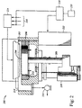
- FIG. 2 is a cross-sectional view of a CVD plasma reactor 200 in which the above plasma reducing process may be performed.
- a reactor may be part of the CENTURA DxZ platform that is manufactured and sold by Applied Materials, Inc. of Santa Clara, California.
- the present invention could be used in other reactors, such as a lamp heated reactor.
- Reactor 200 contains a gas distribution manifold 202, which may be a showerhead, for dispersing process gases through perforated holes (not shown) in the manifold to a substrate or wafer 204 that rests on a substrate support plate or susceptor 206.
- the manifold 202 is connected to a gas panel 224.
- the gas panel 224 is likewise connected to a plurality of process and carrier gas sources 226. Each of the gas sources 226 is connected to a system controller 218.
- the system controller 218 and attendant memory 220 control the activities of the reactor 200. For example, according to the particular process being performed, the controller 218 will send signals to release the appropriate gases at the appropriate flow rates to the gas panel 224.
- the gas panel receives and mixes the gases for distribution to the manifold 202.
- Susceptor 206 is resistivity heated and is mounted on a support stem 208, so that susceptor 206 and the wafer 204 supported on the upper surface of susceptor 206 can be controllably moved by a lift motor 210 between a lower loading/off-loading position and an upper processing position, which is spaced closely adjacent to the manifold 202.
- a lift motor 210 When susceptor 206 and the wafer 204 are in the processing position, they are surrounded by an insulator ring 212.
- gases inlet to manifold 202 are uniformly distributed radially across the substrate surface. The gases exhaust through a port 214 by a vacuum pump system 216.
- the deposition process performed in reactor 200 can be either a thermal process or a plasma enhanced process.
- a controlled plasma is formed adjacent to the wafer by RF energy applied to distribution manifold 202 from RF power supply 222 with susceptor 206 grounded.
- Gas distribution manifold 202 is also an RF electrode, while susceptor 206 is grounded.
- RF power supply 222 can supply either single or mixed frequency RF power to manifold 202 to enhance the decomposition of any reactive species introduced into chamber 200.
- a mixed frequency RF power supply typically supplies power at a high RF frequency (RF1) of 13.56 MHz and at a low RF frequency (RF2) of 350 kHz.
- the above chamber can be used to plasma treat an interface (i.e., reduce an oxide with a reducing agent and particularly a copper oxide with ammonia) and then continuously deposit a second layer upon the interface.
- the reducing agent can be introduced through manifold 202 and be uniformly distributed radially across the wafer surface for the plasma reducing process in the manner described above, followed by the gases exhausting through the port 214.
- the gases necessary to deposit the second layer can be introduced through the manifold 202 without extinguishing the previously formed plasma. That is, the deposition gases alter the characteristics of the plasma thereby allowing for deposition in a seamless manner immediately after reduction.
- the subject invention also includes a method for forming a semiconductor device with a reduced oxidation interface.
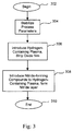
- FIG. 3 depicts a series of method steps 300 in accordance with subject invention.
- the method begins at step 302 and proceeds to step 304 where a stabilization of one or more process parameters is performed. Specifically, conditions such as temperature, pressure, substrate to showerhead spacing and process gas flows are stabilized within a process chamber (i.e., chamber 202).
- the stabilization step 302 is performed for approximately 5-60 seconds, and preferably 15 seconds to attain a process temperature of approximately 400°C, a process pressure of approximately 2.0-6.0 Torr, and preferably 4.2 Torr, a substrate to showerhead spacing of approximately 250-650 mils and preferably 350 mils and a nitrogen gas (N 2 ) flow of approximately 2,000-20,000 sccm and preferably 5,000 sccm.
- a hydrogen containing plasma is introduced to the substrate containing the oxidized interface portions 112. The hydrogen containing plasma chemically reacts with the oxidized interface portions 112 to remove such oxidation and restore the interface portion 112 to its original conductive characteristics.
- the hydrogen containing plasma is preferably formed from a flow of ammonia (NH 3 ) or hydrogen (H 2 ) gas exposed to an appropriate energy source (i.e., DC power source 228).
- Step 306 is conducted for approximately 5-60 seconds and preferably 10 seconds at a temperature of 400°C, a pressure of approximately 2.0-6.0 Torr and preferably 4.2 Torr, a substrate to showerhead spacing of 350 mils and RF power of approximately 50-500 watts and preferably 150 watts and ammonia (NH 3 ) or hydrogen (H 2 ) gas flow of approximately 50-3,000 sccm and preferably 75 ccm and a nitrogen gas (N 2 ) flow rate of approximately 2,000-20,000 sccm and preferably 5,000 sccm.
- step 308 occurs in which one or more insulator forming compounds are introduced to the hydrogen containing plasma to form an insulating layer.
- the insulating layer is in effect the second insulative layer 108 of the device 100.
- step 308 is carried out "in-situ," that is, in the same chamber as the previous steps so as to reduce the likelihood of cross-contamination.
- the second insulative layer need not be fabricated of the same materials as the first insulative layer. Further the second insulative layer may be a plurality of layers formed by a plurality of different process parameters known to those skilled in the art. The following disclosure is exemplary in nature and should not be considered as restricting the scope of the invention.
- the insulator forming compounds are nitride forming compounds which are selected from the group consisting of silane (SiH 4 ), ammonia (NH 3 ) and nitrogen (N 2 ).
- step 308 occurs for approximately 9 seconds at a temperature of 400°C, a pressure of approximately 2.0-6.0 Torr and preferably 4.2 Torr, a substrate to showerhead spacing of approximately 250-650 mils and preferably 550 mils, an RF power of approximately 200-1,000 watts and preferably 460 watts, a silane (SiH 4 ) flow rate of approximately 220 sccm, an ammonia (NH 3 ) flow rate of approximately 50-3,000 sccm and preferably 75 sccm and a nitrogen (N 2 ) flow rate of approximately 2,000-20,000 and preferably 5,000 sccm.
- Table 1 displays an alternate set of process parameters for NH 3 plasma only in both steps 306 and 308.
- Alternate Process Parameters for NH 3 Plasma General Preferred Most Preferred NH 3 Plasma (Step 306) Flow (sccm) 25-1000 25-300 25-100 Pressure (Torr) 1-10 3-7 4-6 Temp (°C) 100-500 200-400 300-400 Spc. (mils) 200-600 300-500 300-400 Power (watts) 100-1000 100-500 100-400 Nitride (Step 308) Flow (sccm) 25-1000 25-300 25-100 Pressure (Torr) 1-10 3-7 4-6 Temp (°C) 100-500 200-400 300-400 Spc. (mils) 200-600 200-600 400-600 Power (watts) 100-1000 100-500 200-400
- the benefits of the subject invention are realized in that oxidation of the interface portion that is conductive is greatly reduced as a result of a chemical reaction. As such, layers deposited thereover have a greater likelihood of adhesion than previously possible with untreated layers or layers treated but still having residual byproducts remaining. Additionally, with a continuous plasma being used, the possibility of copper silicide formation is greatly reduced. That is, copper suicides form when silane is allowed to thermally react at the substrate surface (which contains copper at the interface portions 112). With the back-to-back plasma feature of the subject invention, the silane is broken down into Si and H which allows the nitride to form on the interface before copper suicide can form. Additionally, since the entire process is carried out "in-situ,” there are greatly reduced cross-contamination issues.
Landscapes
- Chemical & Material Sciences (AREA)
- Engineering & Computer Science (AREA)
- Materials Engineering (AREA)
- General Chemical & Material Sciences (AREA)
- Chemical Kinetics & Catalysis (AREA)
- Physics & Mathematics (AREA)
- Mechanical Engineering (AREA)
- Metallurgy (AREA)
- Organic Chemistry (AREA)
- Plasma & Fusion (AREA)
- Optics & Photonics (AREA)
- Internal Circuitry In Semiconductor Integrated Circuit Devices (AREA)
- Formation Of Insulating Films (AREA)
- Drying Of Semiconductors (AREA)
- Element Separation (AREA)
Applications Claiming Priority (2)
| Application Number | Priority Date | Filing Date | Title |
|---|---|---|---|
| US365129 | 1999-07-30 | ||
| US09/365,129 US6355571B1 (en) | 1998-11-17 | 1999-07-30 | Method and apparatus for reducing copper oxidation and contamination in a semiconductor device |
Publications (3)
| Publication Number | Publication Date |
|---|---|
| EP1073106A2 true EP1073106A2 (de) | 2001-01-31 |
| EP1073106A3 EP1073106A3 (de) | 2005-08-24 |
| EP1073106B1 EP1073106B1 (de) | 2008-10-15 |
Family
ID=23437585
Family Applications (1)
| Application Number | Title | Priority Date | Filing Date |
|---|---|---|---|
| EP00109718A Revoked EP1073106B1 (de) | 1999-07-30 | 2000-05-08 | Verfahren zur Verringerung der Oxidation an einer Zwischenschicht einer Halbleiteranordnung |
Country Status (6)
| Country | Link |
|---|---|
| US (5) | US6355571B1 (de) |
| EP (1) | EP1073106B1 (de) |
| JP (1) | JP2001093902A (de) |
| KR (1) | KR100773188B1 (de) |
| DE (1) | DE60040507D1 (de) |
| TW (1) | TW459304B (de) |
Cited By (2)
| Publication number | Priority date | Publication date | Assignee | Title |
|---|---|---|---|---|
| WO2003089681A3 (en) * | 2002-04-18 | 2004-01-22 | Applied Materials Inc | Mixed frequency high temperature nitride cvd process |
| EP2105960A3 (de) * | 2008-03-24 | 2012-04-04 | Air Products and Chemicals, Inc. | Verbesserte Haftung an Kupfer für verbesserten Kupfer-Elektromigrationswiderstand |
Families Citing this family (74)
| Publication number | Priority date | Publication date | Assignee | Title |
|---|---|---|---|---|
| US20010049181A1 (en) | 1998-11-17 | 2001-12-06 | Sudha Rathi | Plasma treatment for cooper oxide reduction |
| US6355571B1 (en) | 1998-11-17 | 2002-03-12 | Applied Materials, Inc. | Method and apparatus for reducing copper oxidation and contamination in a semiconductor device |
| US6821571B2 (en) * | 1999-06-18 | 2004-11-23 | Applied Materials Inc. | Plasma treatment to enhance adhesion and to minimize oxidation of carbon-containing layers |
| JP4554011B2 (ja) * | 1999-08-10 | 2010-09-29 | ルネサスエレクトロニクス株式会社 | 半導体集積回路装置の製造方法 |
| JP2001160558A (ja) * | 1999-12-02 | 2001-06-12 | Nec Corp | 半導体装置の製造方法及び製造装置 |
| JP2001291720A (ja) * | 2000-04-05 | 2001-10-19 | Hitachi Ltd | 半導体集積回路装置および半導体集積回路装置の製造方法 |
| US6794311B2 (en) | 2000-07-14 | 2004-09-21 | Applied Materials Inc. | Method and apparatus for treating low k dielectric layers to reduce diffusion |
| JP2002110679A (ja) * | 2000-09-29 | 2002-04-12 | Hitachi Ltd | 半導体集積回路装置の製造方法 |
| DE10059143B4 (de) * | 2000-11-29 | 2006-12-28 | Advanced Micro Devices, Inc., Sunnyvale | Oberflächenbehandlungs- und Deckschichtverfahren zur Herstellung einer Kupfergrenzfläche in einem Halbleiterbauteil |
| JP2002164428A (ja) * | 2000-11-29 | 2002-06-07 | Hitachi Ltd | 半導体装置およびその製造方法 |
| US6693020B2 (en) * | 2001-03-12 | 2004-02-17 | Motorola, Inc. | Method of preparing copper metallization die for wirebonding |
| US7084070B1 (en) | 2001-03-30 | 2006-08-01 | Lam Research Corporation | Treatment for corrosion in substrate processing |
| US6506677B1 (en) * | 2001-05-02 | 2003-01-14 | Advanced Micro Devices, Inc. | Method of forming capped copper interconnects with reduced hillock formation and improved electromigration resistance |
| US6630406B2 (en) | 2001-05-14 | 2003-10-07 | Axcelis Technologies | Plasma ashing process |
| US6951823B2 (en) * | 2001-05-14 | 2005-10-04 | Axcelis Technologies, Inc. | Plasma ashing process |
| JP2003051481A (ja) * | 2001-08-07 | 2003-02-21 | Hitachi Ltd | 半導体集積回路装置の製造方法 |
| US6797652B1 (en) | 2002-03-15 | 2004-09-28 | Advanced Micro Devices, Inc. | Copper damascene with low-k capping layer and improved electromigration reliability |
| DE10224167B4 (de) * | 2002-05-31 | 2007-01-25 | Advanced Micro Devices, Inc., Sunnyvale | Verfahren zur Herstellung einer Kupferleitung mit erhöhter Widerstandsfähigkeit gegen Elektromigration in einem Halbleiterelement |
| US20040018715A1 (en) * | 2002-07-25 | 2004-01-29 | Applied Materials, Inc. | Method of cleaning a surface of a material layer |
| US6790777B2 (en) * | 2002-11-06 | 2004-09-14 | Texas Instruments Incorporated | Method for reducing contamination, copper reduction, and depositing a dielectric layer on a semiconductor device |
| US7582185B2 (en) * | 2002-12-26 | 2009-09-01 | Canon Kabushiki Kaisha | Plasma-processing apparatus |
| KR100483594B1 (ko) * | 2002-12-27 | 2005-04-15 | 매그나칩 반도체 유한회사 | 반도체 소자의 금속배선 형성방법 |
| US7273808B1 (en) | 2003-02-03 | 2007-09-25 | Novellus Systems, Inc. | Reactive barrier/seed preclean process for damascene process |
| US7604708B2 (en) * | 2003-02-14 | 2009-10-20 | Applied Materials, Inc. | Cleaning of native oxide with hydrogen-containing radicals |
| JP2004247675A (ja) * | 2003-02-17 | 2004-09-02 | Renesas Technology Corp | 半導体装置の製造方法 |
| US8361340B2 (en) * | 2003-04-28 | 2013-01-29 | Air Products And Chemicals, Inc. | Removal of surface oxides by electron attachment |
| US7897029B2 (en) * | 2008-03-04 | 2011-03-01 | Air Products And Chemicals, Inc. | Removal of surface oxides by electron attachment |
| US7387738B2 (en) | 2003-04-28 | 2008-06-17 | Air Products And Chemicals, Inc. | Removal of surface oxides by electron attachment for wafer bumping applications |
| US20040219795A1 (en) * | 2003-05-01 | 2004-11-04 | Taiwan Semiconductor Manufacturing Co. | Method to improve breakdown voltage by H2 plasma treat |
| US7371427B2 (en) * | 2003-05-20 | 2008-05-13 | Applied Materials, Inc. | Reduction of hillocks prior to dielectric barrier deposition in Cu damascene |
| US7723228B2 (en) * | 2003-05-20 | 2010-05-25 | Applied Materials, Inc. | Reduction of hillocks prior to dielectric barrier deposition in Cu damascene |
| US6790778B1 (en) * | 2003-09-10 | 2004-09-14 | Taiwan Semiconductor Manufacturing Co., Ltd. | Method for capping over a copper layer |
| US7309651B2 (en) * | 2003-10-30 | 2007-12-18 | Texas Instruments Incorporated | Method for improving reliability of copper interconnects |
| KR100587659B1 (ko) * | 2003-12-31 | 2006-06-08 | 동부일렉트로닉스 주식회사 | 듀얼 다마신 공정 중 구리 산화 방지 방법 |
| US6897147B1 (en) | 2004-01-15 | 2005-05-24 | Taiwan Semiconductor Manufacturing Company | Solution for copper hillock induced by thermal strain with buffer zone for strain relaxation |
| US20050186339A1 (en) * | 2004-02-20 | 2005-08-25 | Applied Materials, Inc., A Delaware Corporation | Methods and apparatuses promoting adhesion of dielectric barrier film to copper |
| US20050233555A1 (en) * | 2004-04-19 | 2005-10-20 | Nagarajan Rajagopalan | Adhesion improvement for low k dielectrics to conductive materials |
| US7229911B2 (en) * | 2004-04-19 | 2007-06-12 | Applied Materials, Inc. | Adhesion improvement for low k dielectrics to conductive materials |
| US7338903B2 (en) * | 2004-04-24 | 2008-03-04 | Taiwan Semiconductor Manufacturing Co., Ltd. | Sequential reducing plasma and inert plasma pre-treatment method for oxidizable conductor layer |
| US20060081965A1 (en) * | 2004-10-15 | 2006-04-20 | Ju-Ai Ruan | Plasma treatment of an etch stop layer |
| US20070012661A1 (en) * | 2005-07-13 | 2007-01-18 | Vasilyeva Irina V | Silicon nitride passivation layers having oxidized interface |
| KR20090047211A (ko) * | 2007-11-07 | 2009-05-12 | 삼성전자주식회사 | 도전 패턴의 형성 방법 및 이를 이용한 반도체 소자의 제조방법 |
| KR20100099094A (ko) * | 2007-12-27 | 2010-09-10 | 램 리써치 코포레이션 | 베벨 에칭 프로세스에 후속하는 구리 변색 방지 |
| US7737029B2 (en) * | 2008-03-18 | 2010-06-15 | Samsung Electronics Co., Ltd. | Methods of forming metal interconnect structures on semiconductor substrates using oxygen-removing plasmas and interconnect structures formed thereby |
| US20090269507A1 (en) * | 2008-04-29 | 2009-10-29 | Sang-Ho Yu | Selective cobalt deposition on copper surfaces |
| US20100270262A1 (en) * | 2009-04-22 | 2010-10-28 | Applied Materials, Inc. | Etching low-k dielectric or removing resist with a filtered ionized gas |
| US8454850B2 (en) * | 2009-09-02 | 2013-06-04 | Air Products And Chemicals, Inc. | Method for the removal of surface oxides by electron attachment |
| US8329575B2 (en) * | 2010-12-22 | 2012-12-11 | Applied Materials, Inc. | Fabrication of through-silicon vias on silicon wafers |
| US8758638B2 (en) | 2011-05-10 | 2014-06-24 | Applied Materials, Inc. | Copper oxide removal techniques |
| US20140117545A1 (en) * | 2012-10-26 | 2014-05-01 | Globalfoundries Singapore Pte. Ltd | Copper hillock prevention with hydrogen plasma treatment in a dedicated chamber |
| US20140187045A1 (en) * | 2013-01-02 | 2014-07-03 | Applied Materials, Inc. | Silicon nitride gapfill implementing high density plasma |
| US9018108B2 (en) | 2013-01-25 | 2015-04-28 | Applied Materials, Inc. | Low shrinkage dielectric films |
| US9070750B2 (en) | 2013-03-06 | 2015-06-30 | Novellus Systems, Inc. | Methods for reducing metal oxide surfaces to modified metal surfaces using a gaseous reducing environment |
| US9865501B2 (en) | 2013-03-06 | 2018-01-09 | Lam Research Corporation | Method and apparatus for remote plasma treatment for reducing metal oxides on a metal seed layer |
| US8980740B2 (en) | 2013-03-06 | 2015-03-17 | Globalfoundries Inc. | Barrier layer conformality in copper interconnects |
| WO2014150234A1 (en) | 2013-03-15 | 2014-09-25 | Applied Materials, Inc | Processing systems, apparatus, and methods adapted to process substrates in electronic device manufacturing |
| US20150001728A1 (en) * | 2013-06-26 | 2015-01-01 | Taiwan Semiconductor Manufacturing Company, Ltd. | Pre-treatment method for metal-oxide reduction and device formed |
| US20150206798A1 (en) * | 2014-01-17 | 2015-07-23 | Taiwan Semiconductor Manufacturing Company, Ltd. | Interconnect Structure And Method of Forming |
| US9054308B1 (en) | 2014-03-04 | 2015-06-09 | Sandisk 3D Llc | Plasma reduction method for modifying metal oxide stoichiometry in ReRAM |
| US10854472B2 (en) * | 2014-03-19 | 2020-12-01 | Globalfoundries Inc. | Method for forming a metal gate including de-oxidation of an oxidized surface of the metal gate utilizing a reducing agent |
| US9469912B2 (en) | 2014-04-21 | 2016-10-18 | Lam Research Corporation | Pretreatment method for photoresist wafer processing |
| US20150380296A1 (en) * | 2014-06-25 | 2015-12-31 | Lam Research Corporation | Cleaning of carbon-based contaminants in metal interconnects for interconnect capping applications |
| US9472377B2 (en) | 2014-10-17 | 2016-10-18 | Lam Research Corporation | Method and apparatus for characterizing metal oxide reduction |
| US9558955B2 (en) * | 2015-02-03 | 2017-01-31 | Taiwan Semiconductor Manufacturing Co., Ltd. | Formation method of semiconductor device that includes performing hydrogen-containing plasma treatment on metal gate stack |
| US9397011B1 (en) * | 2015-04-13 | 2016-07-19 | Lam Research Corporation | Systems and methods for reducing copper contamination due to substrate processing chambers with components made of alloys including copper |
| US9524905B1 (en) | 2015-08-31 | 2016-12-20 | Sandisk Technologies Llc | Nitrided tungsten via |
| US20180144973A1 (en) * | 2016-11-01 | 2018-05-24 | Applied Materials, Inc. | Electromigration Improvement Using Tungsten For Selective Cobalt Deposition On Copper Surfaces |
| US10443146B2 (en) | 2017-03-30 | 2019-10-15 | Lam Research Corporation | Monitoring surface oxide on seed layers during electroplating |
| KR102331718B1 (ko) | 2017-06-08 | 2021-11-26 | 삼성전자주식회사 | 반도체 장치 제조 방법 |
| US12170310B2 (en) * | 2019-06-26 | 2024-12-17 | Texas Instruments Incorporated | Integrated circuits including composite dielectric layer |
| US11152455B2 (en) | 2019-09-23 | 2021-10-19 | Taiwan Semiconductor Manufacturing Company, Ltd. | Method to reduce breakdown failure in a MIM capacitor |
| US11508617B2 (en) | 2019-10-24 | 2022-11-22 | Applied Materials, Inc. | Method of forming interconnect for semiconductor device |
| US11257677B2 (en) * | 2020-01-24 | 2022-02-22 | Applied Materials, Inc. | Methods and devices for subtractive self-alignment |
| US11430729B2 (en) | 2020-09-16 | 2022-08-30 | Taiwan Semiconductor Manufacturing Company, Ltd. | MIM capacitor with a symmetrical capacitor insulator structure |
Family Cites Families (95)
| Publication number | Priority date | Publication date | Assignee | Title |
|---|---|---|---|---|
| US11A (de) * | 1836-08-10 | |||
| US62A (en) * | 1836-10-20 | Cooking-stove | ||
| US7A (en) * | 1836-08-10 | Thomas Blanchard | Machine for boring holes and cutting lanyard-scores in deadeyes | |
| US1116912A (en) * | 1914-05-14 | 1914-11-10 | Lawson Mfg Company | Gas-burner. |
| US2155862A (en) * | 1936-01-15 | 1939-04-25 | Manifold Supplies Company | Duplicating ink |
| US2290166A (en) * | 1941-02-17 | 1942-07-21 | Edward C Craig | Close fitting, insulating, watertight underwear |
| US2319532A (en) * | 1941-04-29 | 1943-05-18 | Willard Storage Battery Co | Liquid dispensing apparatus |
| US2319533A (en) * | 1941-08-15 | 1943-05-18 | Willard Storage Battery Co | Charging cover |
| US4072724A (en) * | 1975-11-03 | 1978-02-07 | The Goodyear Tire & Rubber Company | Process for preparing hindered alkenyl phenols |
| DE2815074C2 (de) * | 1978-04-07 | 1983-03-03 | Max-Planck-Gesellschaft zur Förderung der Wissenschaften e.V., 3400 Göttingen | Spektralfotometer für medizinische Zwecke |
| JPS55158275A (en) | 1979-05-28 | 1980-12-09 | Hitachi Ltd | Corrosion preventing method for al and al alloy |
| JPS5821324A (ja) | 1981-07-30 | 1983-02-08 | Agency Of Ind Science & Technol | 水素添加した半導体薄膜成長用金属表面基板の前処理方法 |
| US4420386A (en) | 1983-04-22 | 1983-12-13 | White Engineering Corporation | Method for pure ion plating using magnetic fields |
| DE3574997D1 (de) | 1984-03-03 | 1990-02-01 | Stc Plc | Pulsierendes plasmaverfahren. |
| JPS61579A (ja) | 1984-06-14 | 1986-01-06 | Ricoh Co Ltd | 薄膜製造方法 |
| JPS619579A (ja) | 1984-06-25 | 1986-01-17 | Nippon Steel Corp | 鉄鋼構造物の防食工法 |
| JPS62158859A (ja) | 1986-01-07 | 1987-07-14 | Sumitomo Electric Ind Ltd | 前処理方法 |
| US5000113A (en) | 1986-12-19 | 1991-03-19 | Applied Materials, Inc. | Thermal CVD/PECVD reactor and use for thermal chemical vapor deposition of silicon dioxide and in-situ multi-step planarized process |
| US4849797A (en) * | 1987-01-23 | 1989-07-18 | Hosiden Electronics Co., Ltd. | Thin film transistor |
| US5121706A (en) | 1987-10-16 | 1992-06-16 | The Curators Of The University Of Missouri | Apparatus for applying a composite insulative coating to a substrate |
| JPH01116912A (ja) | 1987-10-29 | 1989-05-09 | Sony Corp | 磁気抵抗効果型磁気ヘッド |
| US4994410A (en) | 1988-04-04 | 1991-02-19 | Motorola, Inc. | Method for device metallization by forming a contact plug and interconnect using a silicide/nitride process |
| US5232872A (en) | 1989-05-09 | 1993-08-03 | Fujitsu Limited | Method for manufacturing semiconductor device |
| JPH0338953A (ja) | 1989-07-05 | 1991-02-20 | Nec Corp | 電話機のダイアル送出用集積回路 |
| DE69025244T2 (de) | 1989-08-25 | 1996-06-27 | Applied Materials Inc | Reinigungsverfahren für eine Anlage zur Behandlung von Halbleiterscheiben |
| US4980196A (en) | 1990-02-14 | 1990-12-25 | E. I. Du Pont De Nemours And Company | Method of coating steel substrate using low temperature plasma processes and priming |
| JPH0445534A (ja) | 1990-06-12 | 1992-02-14 | Sony Corp | 銅薄膜の選択的エッチング方法 |
| JP2646811B2 (ja) | 1990-07-13 | 1997-08-27 | ソニー株式会社 | ドライエッチング方法 |
| FR2666324B1 (fr) | 1990-09-03 | 1993-04-09 | Saint Gobain Vitrage Int | Couches minces de nitrure de silicium a proprietes ameliorees. |
| DE4034842A1 (de) | 1990-11-02 | 1992-05-07 | Thyssen Edelstahlwerke Ag | Verfahren zur plasmachemischen reinigung fuer eine anschliessende pvd oder pecvd beschichtung |
| US5232871A (en) | 1990-12-27 | 1993-08-03 | Intel Corporation | Method for forming a titanium nitride barrier layer |
| JP3038953B2 (ja) | 1991-02-28 | 2000-05-08 | ソニー株式会社 | 配線形成方法 |
| US5324360A (en) | 1991-05-21 | 1994-06-28 | Canon Kabushiki Kaisha | Method for producing non-monocrystalline semiconductor device and apparatus therefor |
| JPH05308107A (ja) | 1991-07-01 | 1993-11-19 | Sumitomo Electric Ind Ltd | 半導体装置及びその製作方法 |
| JPH05144811A (ja) | 1991-11-22 | 1993-06-11 | Hitachi Ltd | 薄膜半導体装置及びその製造方法 |
| WO1993017453A2 (en) | 1992-02-26 | 1993-09-02 | Materials Research Corporation | Ammonia plasma treatment of silicide contact surfaces in semiconductor devices |
| JPH0697111A (ja) | 1992-09-11 | 1994-04-08 | Sony Corp | バリアメタルの形成方法 |
| JPH06204191A (ja) | 1992-11-10 | 1994-07-22 | Sony Corp | 金属プラグ形成後の表面処理方法 |
| US5409543A (en) | 1992-12-22 | 1995-04-25 | Sandia Corporation | Dry soldering with hot filament produced atomic hydrogen |
| JPH0763105B2 (ja) | 1993-02-12 | 1995-07-05 | 日本電気株式会社 | 印刷配線板の製造方法 |
| JP3399583B2 (ja) | 1993-04-06 | 2003-04-21 | 東京エレクトロン株式会社 | 半導体装置の製造方法 |
| KR100326488B1 (ko) | 1993-06-21 | 2002-06-20 | 조셉 제이. 스위니 | 플라즈마화학기상증착법 |
| JPH0793276B2 (ja) | 1993-12-14 | 1995-10-09 | アプライド マテリアルズ インコーポレイテッド | 薄膜形成前処理方法および薄膜形成方法 |
| JP2837087B2 (ja) | 1993-12-28 | 1998-12-14 | アプライド マテリアルズ インコーポレイテッド | 薄膜形成方法 |
| US6475903B1 (en) * | 1993-12-28 | 2002-11-05 | Intel Corporation | Copper reflow process |
| US5738956A (en) * | 1994-01-28 | 1998-04-14 | Kyowa Hakko Kogyo | Agent for maintaining and recovering the function of lead storage battery and electrolyte for lead storage battery using the same |
| US5451263A (en) | 1994-02-03 | 1995-09-19 | Harris Corporation | Plasma cleaning method for improved ink brand permanency on IC packages with metallic parts |
| US5441768A (en) | 1994-02-08 | 1995-08-15 | Applied Materials, Inc. | Multi-step chemical vapor deposition method for thin film transistors |
| IT1271636B (it) | 1994-05-04 | 1997-06-04 | Alcatel Italia | Metodo per la preparazione e la passivazione degli specchi terminali di laser a semiconduttore ad alta potenza di emissione e relativo dispositivo |
| US5975912A (en) * | 1994-06-03 | 1999-11-02 | Materials Research Corporation | Low temperature plasma-enhanced formation of integrated circuits |
| US5665640A (en) * | 1994-06-03 | 1997-09-09 | Sony Corporation | Method for producing titanium-containing thin films by low temperature plasma-enhanced chemical vapor deposition using a rotating susceptor reactor |
| KR0144956B1 (ko) | 1994-06-10 | 1998-08-17 | 김광호 | 반도체 장치의 배선 구조 및 그 형성방법 |
| JP3326974B2 (ja) | 1994-07-28 | 2002-09-24 | ソニー株式会社 | 多層配線の形成方法および半導体装置の製造方法 |
| US5736002A (en) | 1994-08-22 | 1998-04-07 | Sharp Microelectronics Technology, Inc. | Methods and equipment for anisotropic, patterned conversion of copper into selectively removable compounds and for removal of same |
| DE69531980T2 (de) | 1994-08-23 | 2004-07-29 | At & T Corp. | Metallisierung von keramischen Materialien durch Auftrag einer haftenden reduzierbaren Schicht |
| JP2809113B2 (ja) | 1994-09-29 | 1998-10-08 | 日本電気株式会社 | 半導体装置の製造方法 |
| JPH08186085A (ja) | 1994-12-28 | 1996-07-16 | Nec Corp | 半導体装置の製造方法 |
| US5599736A (en) * | 1995-06-28 | 1997-02-04 | Vanguard International Semiconductor Corporation | Fabrication method for polysilicon contact plugs |
| BE1009839A3 (fr) | 1995-12-20 | 1997-10-07 | Cockerill Rech & Dev | Procede et dispositif pour le nettoyage d'un substrat metallique. |
| US6013574A (en) * | 1996-01-30 | 2000-01-11 | Advanced Micro Devices, Inc. | Method of forming low resistance contact structures in vias arranged between two levels of interconnect lines |
| US5843847A (en) | 1996-04-29 | 1998-12-01 | Applied Materials, Inc. | Method for etching dielectric layers with high selectivity and low microloading |
| US5780163A (en) | 1996-06-05 | 1998-07-14 | Dow Corning Corporation | Multilayer coating for microelectronic devices |
| JPH1019244A (ja) | 1996-06-27 | 1998-01-23 | Nkk Corp | ドレン排出装置、ドレン排出装置を備える交番燃焼炉及び交番燃焼炉のドレン排出方法 |
| US5970378A (en) | 1996-09-03 | 1999-10-19 | Taiwan Semiconductor Manufacturing Company, Ltd. | Multi-step plasma treatment process for forming low resistance titanium nitride layer |
| US5801098A (en) | 1996-09-03 | 1998-09-01 | Motorola, Inc. | Method of decreasing resistivity in an electrically conductive layer |
| GB2319533B (en) | 1996-11-22 | 2001-06-06 | Trikon Equip Ltd | Methods of forming a barrier layer |
| GB2319532B (en) | 1996-11-22 | 2001-01-31 | Trikon Equip Ltd | Method and apparatus for treating a semiconductor wafer |
| KR19980064441A (ko) | 1996-12-20 | 1998-10-07 | 윌리엄비.켐플러 | 전도물질을 반도체 소자 표면에 선택적으로 결합시키는 방법 |
| JP4142753B2 (ja) | 1996-12-26 | 2008-09-03 | 株式会社東芝 | スパッタターゲット、スパッタ装置、半導体装置およびその製造方法 |
| DE19702124A1 (de) | 1997-01-22 | 1998-07-23 | Linde Ag | Verfahren und Vorrichtung zum Reinigen, Aktivieren Benetzen und/oder Beschichten der Oberflächen von Werkstücken |
| US5834371A (en) * | 1997-01-31 | 1998-11-10 | Tokyo Electron Limited | Method and apparatus for preparing and metallizing high aspect ratio silicon semiconductor device contacts to reduce the resistivity thereof |
| DE19717698A1 (de) | 1997-04-26 | 1998-10-29 | Fraunhofer Ges Forschung | Verfahren und Vorrichtung zur Reinigung von Aktivierung von elektrischen Leiterbahnen und Platinenoberflächen |
| JPH1116912A (ja) | 1997-06-25 | 1999-01-22 | Hitachi Ltd | 半導体集積回路装置の製造方法および半導体集積回路装置の製造装置 |
| US6872429B1 (en) * | 1997-06-30 | 2005-03-29 | Applied Materials, Inc. | Deposition of tungsten nitride using plasma pretreatment in a chemical vapor deposition chamber |
| US5893752A (en) * | 1997-12-22 | 1999-04-13 | Motorola, Inc. | Process for forming a semiconductor device |
| US5821168A (en) * | 1997-07-16 | 1998-10-13 | Motorola, Inc. | Process for forming a semiconductor device |
| US6100184A (en) * | 1997-08-20 | 2000-08-08 | Sematech, Inc. | Method of making a dual damascene interconnect structure using low dielectric constant material for an inter-level dielectric layer |
| US6143640A (en) * | 1997-09-23 | 2000-11-07 | International Business Machines Corporation | Method of fabricating a stacked via in copper/polyimide beol |
| US6071813A (en) * | 1997-10-20 | 2000-06-06 | Advanced Micro Devices, Inc. | Method and system for electrical coupling to copper interconnects |
| TW507015B (en) * | 1997-12-02 | 2002-10-21 | Applied Materials Inc | In-situ, preclean of wafers prior to a chemical vapor deposition titanium deposition step |
| US6033584A (en) * | 1997-12-22 | 2000-03-07 | Advanced Micro Devices, Inc. | Process for reducing copper oxide during integrated circuit fabrication |
| JP3501937B2 (ja) | 1998-01-30 | 2004-03-02 | 富士通株式会社 | 半導体装置の製造方法 |
| FR2775986B1 (fr) | 1998-03-10 | 2000-05-05 | Air Liquide | Procede et installation de traitement de surface d'une piece metallique |
| US6174810B1 (en) * | 1998-04-06 | 2001-01-16 | Motorola, Inc. | Copper interconnect structure and method of formation |
| US6319728B1 (en) * | 1998-06-05 | 2001-11-20 | Applied Materials, Inc. | Method for treating a deposited film for resistivity reduction |
| KR100290835B1 (ko) * | 1998-06-23 | 2001-07-12 | 윤종용 | 반도체소자의제조방법 |
| US6492266B1 (en) * | 1998-07-09 | 2002-12-10 | Advanced Micro Devices, Inc. | Method of forming reliable capped copper interconnects |
| US6303505B1 (en) * | 1998-07-09 | 2001-10-16 | Advanced Micro Devices, Inc. | Copper interconnect with improved electromigration resistance |
| US6287977B1 (en) * | 1998-07-31 | 2001-09-11 | Applied Materials, Inc. | Method and apparatus for forming improved metal interconnects |
| US6172421B1 (en) * | 1998-08-11 | 2001-01-09 | Advanced Micro Devices, Inc. | Semiconductor device having an intermetallic layer on metal interconnects |
| US6355571B1 (en) | 1998-11-17 | 2002-03-12 | Applied Materials, Inc. | Method and apparatus for reducing copper oxidation and contamination in a semiconductor device |
| US6097111A (en) * | 1998-12-29 | 2000-08-01 | Anrod; Stephen C. | Mode selectable power receptacle |
| US6251775B1 (en) | 1999-04-23 | 2001-06-26 | International Business Machines Corporation | Self-aligned copper silicide formation for improved adhesion/electromigration |
| US6365527B1 (en) | 2000-10-06 | 2002-04-02 | United Microelectronics Corp. | Method for depositing silicon carbide in semiconductor devices |
| US20040155268A1 (en) * | 2003-02-06 | 2004-08-12 | Infineon Technologies North America Corp. | Method and apparatus for improving the electrical resistance of conductive paths |
-
1999
- 1999-07-30 US US09/365,129 patent/US6355571B1/en not_active Expired - Lifetime
-
2000
- 2000-05-05 TW TW089108656A patent/TW459304B/zh not_active IP Right Cessation
- 2000-05-08 EP EP00109718A patent/EP1073106B1/de not_active Revoked
- 2000-05-08 DE DE60040507T patent/DE60040507D1/de not_active Expired - Fee Related
- 2000-07-29 KR KR1020000043933A patent/KR100773188B1/ko not_active Expired - Lifetime
- 2000-07-31 JP JP2000231957A patent/JP2001093902A/ja not_active Withdrawn
-
2001
- 2001-12-07 US US10/013,182 patent/US6700202B2/en not_active Expired - Lifetime
-
2003
- 2003-09-04 US US10/655,438 patent/US6946401B2/en not_active Expired - Fee Related
-
2005
- 2005-06-29 US US11/169,337 patent/US20050263900A1/en not_active Abandoned
-
2008
- 2008-10-24 US US12/257,806 patent/US8183150B2/en not_active Expired - Fee Related
Cited By (3)
| Publication number | Priority date | Publication date | Assignee | Title |
|---|---|---|---|---|
| WO2003089681A3 (en) * | 2002-04-18 | 2004-01-22 | Applied Materials Inc | Mixed frequency high temperature nitride cvd process |
| EP2105960A3 (de) * | 2008-03-24 | 2012-04-04 | Air Products and Chemicals, Inc. | Verbesserte Haftung an Kupfer für verbesserten Kupfer-Elektromigrationswiderstand |
| TWI479567B (zh) * | 2008-03-24 | 2015-04-01 | 氣體產品及化學品股份公司 | 改良的對銅的黏著力及銅電遷移阻力 |
Also Published As
| Publication number | Publication date |
|---|---|
| US20020081856A1 (en) | 2002-06-27 |
| US6700202B2 (en) | 2004-03-02 |
| EP1073106A3 (de) | 2005-08-24 |
| EP1073106B1 (de) | 2008-10-15 |
| US20050263900A1 (en) | 2005-12-01 |
| US8183150B2 (en) | 2012-05-22 |
| US6355571B1 (en) | 2002-03-12 |
| US6946401B2 (en) | 2005-09-20 |
| JP2001093902A (ja) | 2001-04-06 |
| US20090050902A1 (en) | 2009-02-26 |
| KR100773188B1 (ko) | 2007-11-02 |
| KR20010039772A (ko) | 2001-05-15 |
| DE60040507D1 (de) | 2008-11-27 |
| US20040046260A1 (en) | 2004-03-11 |
| TW459304B (en) | 2001-10-11 |
Similar Documents
| Publication | Publication Date | Title |
|---|---|---|
| US6355571B1 (en) | Method and apparatus for reducing copper oxidation and contamination in a semiconductor device | |
| US6218301B1 (en) | Deposition of tungsten films from W(CO)6 | |
| US6436819B1 (en) | Nitrogen treatment of a metal nitride/metal stack | |
| JP4901004B2 (ja) | 基板表面上の酸化銅を除去する方法 | |
| US6949450B2 (en) | Method for integrated in-situ cleaning and subsequent atomic layer deposition within a single processing chamber | |
| KR100743775B1 (ko) | 확산을 감소시키도록 낮은 유전상수 k의 유전층을 처리하기 위한 방법 및 장치 | |
| US9633896B1 (en) | Methods for formation of low-k aluminum-containing etch stop films | |
| US20020155219A1 (en) | Plasma treatment of a titanium nitride film formed by chemical vapor deposition | |
| US20040248404A1 (en) | Reactive preclean prior to metallization for sub-quarter micron application | |
| US20020114886A1 (en) | Method of tisin deposition using a chemical vapor deposition process | |
| KR20030001939A (ko) | 반도체소자의 장벽층 형성 방법 및 장치 | |
| EP1084512A1 (de) | Plasmabehandlung für ex-situ-füllung eines kontakts | |
| KR20010031857A (ko) | 텅스텐 플러그 기술에서 PE-CVD-Ti 및 동일 반응계플라즈마 질화법을 이용하여 질화티탄막 부착 단계를제거하는 방법 | |
| WO2002046489A1 (en) | Method for integrated in-situ cleaning and subsequent atomic layer deposition within a single processing chamber | |
| US6365495B2 (en) | Method for performing metallo-organic chemical vapor deposition of titanium nitride at reduced temperature | |
| US20020168468A1 (en) | Method of TiSiN deposition using a chemical vapor deposition (CVD) process | |
| US6753258B1 (en) | Integration scheme for dual damascene structure | |
| KR20110013418A (ko) | 유전성 및 전도성 층 사이의 접착 및 전자 이동 개선 | |
| US20020142104A1 (en) | Plasma treatment of organosilicate layers | |
| WO2002021593A9 (en) | Method of forming titanium nitride (tin) films using metal-organic chemical vapor deposition (mocvd) | |
| US6632737B1 (en) | Method for enhancing the adhesion of a barrier layer to a dielectric | |
| KR20260005999A (ko) | 기판 처리 방법 및 기판 처리 장치 |
Legal Events
| Date | Code | Title | Description |
|---|---|---|---|
| PUAI | Public reference made under article 153(3) epc to a published international application that has entered the european phase |
Free format text: ORIGINAL CODE: 0009012 |
|
| AK | Designated contracting states |
Kind code of ref document: A2 Designated state(s): AT BE CH CY DE DK ES FI FR GB GR IE IT LI LU MC NL PT SE |
|
| AX | Request for extension of the european patent |
Free format text: AL;LT;LV;MK;RO;SI |
|
| PUAL | Search report despatched |
Free format text: ORIGINAL CODE: 0009013 |
|
| AK | Designated contracting states |
Kind code of ref document: A3 Designated state(s): AT BE CH CY DE DK ES FI FR GB GR IE IT LI LU MC NL PT SE |
|
| AX | Request for extension of the european patent |
Extension state: AL LT LV MK RO SI |
|
| 17P | Request for examination filed |
Effective date: 20060220 |
|
| AKX | Designation fees paid |
Designated state(s): DE FR GB |
|
| 17Q | First examination report despatched |
Effective date: 20071025 |
|
| GRAP | Despatch of communication of intention to grant a patent |
Free format text: ORIGINAL CODE: EPIDOSNIGR1 |
|
| RTI1 | Title (correction) |
Free format text: METHOD FOR REDUCING OXIDATION OF AN INTERFACE OF A SEMICONDUCTOR DEVICE |
|
| GRAS | Grant fee paid |
Free format text: ORIGINAL CODE: EPIDOSNIGR3 |
|
| GRAA | (expected) grant |
Free format text: ORIGINAL CODE: 0009210 |
|
| AK | Designated contracting states |
Kind code of ref document: B1 Designated state(s): DE FR GB |
|
| REG | Reference to a national code |
Ref country code: GB Ref legal event code: FG4D |
|
| REF | Corresponds to: |
Ref document number: 60040507 Country of ref document: DE Date of ref document: 20081127 Kind code of ref document: P |
|
| PLBI | Opposition filed |
Free format text: ORIGINAL CODE: 0009260 |
|
| PLAX | Notice of opposition and request to file observation + time limit sent |
Free format text: ORIGINAL CODE: EPIDOSNOBS2 |
|
| 26 | Opposition filed |
Opponent name: DIGITAL SIMPLEX PTE LTD. Effective date: 20090714 |
|
| PGFP | Annual fee paid to national office [announced via postgrant information from national office to epo] |
Ref country code: DE Payment date: 20090630 Year of fee payment: 10 |
|
| PLAF | Information modified related to communication of a notice of opposition and request to file observations + time limit |
Free format text: ORIGINAL CODE: EPIDOSCOBS2 |
|
| GBPC | Gb: european patent ceased through non-payment of renewal fee |
Effective date: 20090508 |
|
| REG | Reference to a national code |
Ref country code: FR Ref legal event code: ST Effective date: 20100129 |
|
| PLBB | Reply of patent proprietor to notice(s) of opposition received |
Free format text: ORIGINAL CODE: EPIDOSNOBS3 |
|
| PG25 | Lapsed in a contracting state [announced via postgrant information from national office to epo] |
Ref country code: FR Free format text: LAPSE BECAUSE OF NON-PAYMENT OF DUE FEES Effective date: 20090602 |
|
| PG25 | Lapsed in a contracting state [announced via postgrant information from national office to epo] |
Ref country code: GB Free format text: LAPSE BECAUSE OF NON-PAYMENT OF DUE FEES Effective date: 20090508 |
|
| PG25 | Lapsed in a contracting state [announced via postgrant information from national office to epo] |
Ref country code: DE Free format text: LAPSE BECAUSE OF NON-PAYMENT OF DUE FEES Effective date: 20101201 |
|
| RDAF | Communication despatched that patent is revoked |
Free format text: ORIGINAL CODE: EPIDOSNREV1 |
|
| RDAG | Patent revoked |
Free format text: ORIGINAL CODE: 0009271 |
|
| STAA | Information on the status of an ep patent application or granted ep patent |
Free format text: STATUS: PATENT REVOKED |
|
| 27W | Patent revoked |
Effective date: 20111014 |