EP1076244A1 - Radar a ondes continues modulees en frequence - Google Patents
Radar a ondes continues modulees en frequence Download PDFInfo
- Publication number
- EP1076244A1 EP1076244A1 EP99910679A EP99910679A EP1076244A1 EP 1076244 A1 EP1076244 A1 EP 1076244A1 EP 99910679 A EP99910679 A EP 99910679A EP 99910679 A EP99910679 A EP 99910679A EP 1076244 A1 EP1076244 A1 EP 1076244A1
- Authority
- EP
- European Patent Office
- Prior art keywords
- antenna elements
- beat signal
- wave
- signal
- frequency
- Prior art date
- Legal status (The legal status is an assumption and is not a legal conclusion. Google has not performed a legal analysis and makes no representation as to the accuracy of the status listed.)
- Granted
Links
Images



Classifications
-
- G—PHYSICS
- G01—MEASURING; TESTING
- G01S—RADIO DIRECTION-FINDING; RADIO NAVIGATION; DETERMINING DISTANCE OR VELOCITY BY USE OF RADIO WAVES; LOCATING OR PRESENCE-DETECTING BY USE OF THE REFLECTION OR RERADIATION OF RADIO WAVES; ANALOGOUS ARRANGEMENTS USING OTHER WAVES
- G01S13/00—Systems using the reflection or reradiation of radio waves, e.g. radar systems; Analogous systems using reflection or reradiation of waves whose nature or wavelength is irrelevant or unspecified
- G01S13/02—Systems using reflection of radio waves, e.g. primary radar systems; Analogous systems
- G01S13/06—Systems determining position data of a target
- G01S13/08—Systems for measuring distance only
- G01S13/32—Systems for measuring distance only using transmission of continuous waves, whether amplitude-, frequency-, or phase-modulated, or unmodulated
- G01S13/34—Systems for measuring distance only using transmission of continuous waves, whether amplitude-, frequency-, or phase-modulated, or unmodulated using transmission of continuous, frequency-modulated waves while heterodyning the received signal, or a signal derived therefrom, with a locally-generated signal related to the contemporaneously transmitted signal
-
- G—PHYSICS
- G01—MEASURING; TESTING
- G01S—RADIO DIRECTION-FINDING; RADIO NAVIGATION; DETERMINING DISTANCE OR VELOCITY BY USE OF RADIO WAVES; LOCATING OR PRESENCE-DETECTING BY USE OF THE REFLECTION OR RERADIATION OF RADIO WAVES; ANALOGOUS ARRANGEMENTS USING OTHER WAVES
- G01S13/00—Systems using the reflection or reradiation of radio waves, e.g. radar systems; Analogous systems using reflection or reradiation of waves whose nature or wavelength is irrelevant or unspecified
- G01S13/02—Systems using reflection of radio waves, e.g. primary radar systems; Analogous systems
- G01S13/06—Systems determining position data of a target
- G01S13/08—Systems for measuring distance only
- G01S13/32—Systems for measuring distance only using transmission of continuous waves, whether amplitude-, frequency-, or phase-modulated, or unmodulated
- G01S13/34—Systems for measuring distance only using transmission of continuous waves, whether amplitude-, frequency-, or phase-modulated, or unmodulated using transmission of continuous, frequency-modulated waves while heterodyning the received signal, or a signal derived therefrom, with a locally-generated signal related to the contemporaneously transmitted signal
- G01S13/345—Systems for measuring distance only using transmission of continuous waves, whether amplitude-, frequency-, or phase-modulated, or unmodulated using transmission of continuous, frequency-modulated waves while heterodyning the received signal, or a signal derived therefrom, with a locally-generated signal related to the contemporaneously transmitted signal using triangular modulation
-
- G—PHYSICS
- G01—MEASURING; TESTING
- G01S—RADIO DIRECTION-FINDING; RADIO NAVIGATION; DETERMINING DISTANCE OR VELOCITY BY USE OF RADIO WAVES; LOCATING OR PRESENCE-DETECTING BY USE OF THE REFLECTION OR RERADIATION OF RADIO WAVES; ANALOGOUS ARRANGEMENTS USING OTHER WAVES
- G01S13/00—Systems using the reflection or reradiation of radio waves, e.g. radar systems; Analogous systems using reflection or reradiation of waves whose nature or wavelength is irrelevant or unspecified
- G01S13/02—Systems using reflection of radio waves, e.g. primary radar systems; Analogous systems
- G01S2013/0236—Special technical features
- G01S2013/0245—Radar with phased array antenna
Definitions
- the present invention relates to an FM-CW radar apparatus using a frequency-modulated continuous wave as a transmitted wave and, more particularly, to the FM-CW radar apparatus that can accomplish a beam scan by digital beamforming (DBF).
- DBF digital beamforming
- An example of the DBF radar apparatus is one described in Japanese Patent Application Laid-Open No. 6-88869.
- an RF amplifier, a mixer, a filter, and an A/D converter are connected to each of antenna elements constituting an array antenna, digital signals outputted from the respective A/D converters are read into a digital beamforming processor, and the digital beamforming processor carries out the digital beamforming operation, based thereon.
- the radar apparatus uses high-frequency electromagnetic waves such as microwaves or millimeter waves, but analog devices (such as the RF amplifiers and mixers) operating at such high frequencies are very expensive.
- the conventional radar apparatus described above necessitates a number of analog devices, because such analog devices are given to each of the antenna elements. Therefore, the production cost becomes inevitably high. Particularly, it is conceivable as a means for improving the performance that the number of antenna elements is increased, but the increase of the antenna elements also increases the number of high-frequency analog devices attendant thereon, thereby increasing the cost. It was thus difficult to increase the number of antenna elements. In addition, the increase of analog devices also increases the scale of the radar apparatus.
- An object of the present invention is to provide an FM-CW radar apparatus including the minimum number of analog devices, regardless of the number of antenna elements.
- the FM-CW radar apparatus of the present invention comprises a transmitter section, a receiver section, and a signal processing section.
- the transmitter section transmits a frequency-modulated continuous wave as a transmitted wave.
- the receiver section receives radio waves resulting from re-radiation from a target, as received waves, through a receiving antenna comprised of an array of antenna elements, generates a beat signal which is a difference between the transmitted wave and a received wave in each of channels of the respective antenna elements, and converts this beat signal to a digital beat signal by A/D conversion.
- the signal processing section executes the digital beamforming operation with the digital beat signals to detect the target from the result thereof.
- the receiver section comprises switch means for selectively connecting either one of the antenna elements to a circuit for generating a beat signal and this switch means connects only part of the antenna elements to the beat signal generating circuit in one period of repetition periods of frequency modulation.
- the switch means selectively connects either one of the antenna elements in sequence to the circuit for generating the beat signal, the received waves through the respective antenna elements can be supplied in time division to the circuit for generating the beat signal. There is thus no need to prepare the high-frequency devices, such as the mixer circuit etc. for downconversion of the received wave, for each of the antenna elements, and only one set will suffice.
- the switching frequency may be lower than that in the case wherein all the antenna elements are connected to the beat signal generating circuit in one of repetition periods of the frequency modulation.
- an A/D conversion rate may also be reduced with decrease of the switching frequency.
- the switch means should select one antenna element as a reference antenna element in each of repetition periods of the frequency modulation and that the signal processing section should correct phases of waves received by the antenna elements other than the reference antenna element, based on a phase difference of a wave received by the reference antenna element in each of repetition periods of the frequency modulation.
- the distance to the target may vary during a time difference. In that case, there will occur a difference between phases of received waves. Namely, sufficient simultaneity of reception is not assured for every antenna element.
- the apparatus since the apparatus is constructed to detect a phase difference of a signal from the reference antenna element in each period and to correct phases of signals of the antenna elements other than the reference antenna element, based on this phase difference, the apparatus may perform the DBF synthesis almost equivalent to that in the case wherein the signals from all the antenna elements are read in in one period.
- Fig. 1 is a structural diagram to show a radar apparatus as an embodiment of the present invention.
- This radar apparatus is an FM-CW radar apparatus designed to use a frequency-modulated (FM) continuous wave (CW) as a transmitted signal and a DBF radar apparatus designed to execute the digital beamforming operation.
- FM frequency-modulated
- CW continuous wave
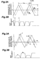
- Figs. 2A, 2B, 3A, and 3B are waveform diagrams to show the principle of detection of the FM-CW radar.
- Fig. 2A is a graph to show change in the frequency of the transmitted signal and change in the frequency of a received signal resulting from re-radiation from a target at the position of distance R and with the relative velocity of zero, in which the frequencies are on the vertical axis while the time on the horizontal axis.
- the solid line indicates the frequencies of the transmitted signal and the dashed line the frequencies of the received signal.
- the transmitted signal is a modulated signal resulting from triangular frequency modulation of a continuous wave.
- the center frequency of the modulated wave is f0
- a frequency shift width is ⁇ F
- the repetition frequency of the triangular wave is fm.
- Fig. 3A is a graph to show change in the frequency of the transmitted signal and change in the frequency of a received signal where the target has a relative velocity V except for zero, in which the solid line indicates the frequencies of the transmitted signal while the dotted line the frequencies of the received signal.
- the definition of the transmitted signal and the coordinate axes is the same as in Fig. 2A.
- the received signal has the time lag T according to the distance with respect to the transmitted signal and a frequency deviation D corresponding to the relative velocity.
- the frequencies of the received signal deviate upward in the graph, which means that the target is approaching.
- a beat signal can be obtained by mixing part of the transmitted signal in such a received signal.
- Fig. 2B and Fig. 3B are graphs to show beat frequencies when the relative velocity of the target is zero and V (V ⁇ 0), respectively, and their time axis (horizontal axis) is timed with that in Fig. 2A and Fig. 3A.
- fr the beat frequency at the relative velocity of zero
- fd the Doppler frequency based on the relative velocity
- fb1 the beat frequency in a frequency-increasing interval (up interval)
- fb2 the beat frequency in a frequency-decreasing interval (down interval). Then the following equations hold.
- fr and fd can be computed from the following equations (3) and (4) if the beat frequencies fb1 and fb2 in the up interval and in the down interval of a modulation cycle are measured separately.
- fr (fb1 + fb2)/2
- fd (fb2 - fb1)/2
- R (C/(4 ⁇ ⁇ F ⁇ fm))
- fr V (C/(2 ⁇ f0)) ⁇ fd
- C represents the speed of light.
- the direction, the distance, and the velocity of the target may be detected by successively computing the distances R and velocities V while carrying out the beam scan. This is the principle of the FM-CW radar.
- the FM-CW radar apparatus of the present embodiment illustrated in Fig. 1 is also the DBF radar apparatus.
- this FM-CW radar apparatus is designed to use an array antenna composed of a plurality of antenna elements as a receiving antenna, digitize signals received by the respective antenna elements, convert the phase and amplitude of each signal in the signal processing section of a subsequent stage, and further execute composition of signals of all the antenna element channels, thereby forming directivity of the receiving antenna.
- a desired beam scan may thus be executed by carrying out the conversion with appropriate change in conversion amounts of the phase and amplitude from the signals once read in.
- This radar apparatus is provided with a transmitter section 1, an array antenna 2, a changeover switch section 3, a receiving circuit section 4, and a digital signal processing section 5.
- the array antenna 2, the changeover switch section 3, and the receiving circuit section 4 compose a receiver section.
- the transmitter section 1 is composed of a voltage-controlled oscillator 11 having the center frequency of f0 (for example, 76 GHz), a buffer amplifier 12, a transmission antenna 13, and an RF amplifier 14.
- the oscillator 11 outputs the modulated wave (transmitted signal) of f0 ⁇ ⁇ F/2 , based on a control voltage outputted from a dc power supply for modulation not illustrated.
- the modulated wave is amplified by the buffer amplifier 12 and is radiated as an electromagnetic wave from the transmission antenna 13. Part of the transmitted signal is amplified by the RF amplifier 14 to be supplied as a local signal for downconversion.
- the array antenna 2 for reception has nine antenna elements corresponding to respective channels from the first channel (CH1) to the ninth channel (CH9).
- the changeover switch section 3 is comprised of a switch body 31 and a switch control 32.
- the switch body 31 has nine input terminals and one output terminal and each antenna element of the array antenna 2 is connected to a corresponding input terminal.
- the output terminal is designed to be connected to either one of the input terminals and the connection thereof is changed over properly in response to a changeover signal from the switch control 32.
- the changeover of connection is carried out electrically on the circuitry and the sequence of changeover will be described hereinafter.
- the receiving circuit section 4 is composed of an RF amplifier 41, a mixer 42, an amplifier 43, a filter 44, and an A/D converter 45.
- the RF amplifier 41 amplifies a signal outputted from the output terminal of the switch body 31, which is a signal received by either antenna element of the array antenna 2, and the mixer 42 mixes the amplified signal with part of the transmitted signal from the RF amplifier 14.
- the received signal is downconverted by this mixing to generate a beat signal as a difference signal between the transmitted signal and the received signal.
- the beat signal is supplied via the amplifier 43 and the low-pass filter 44 to the A/D converter 45 to be converted into a digital signal at the timing of a signal from the switch control 32, i.e., at the timing of a clock signal fsw for execution of connection changeover in the switch body 31.
- the digital signal processing section 5 executes the digital beamforming (DBF) operation with digital beat signals from the A/D converter 45 to detect the target from the result thereof.
- DBF digital beamforming
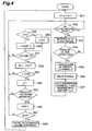
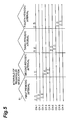
- Fig. 4 is a flowchart to show the operation of the FM-CW radar apparatus and Fig. 5 is a timing chart to show the changeover timing sequence of the changeover switch section 3.
- i indicates a channel number of each antenna element, j a sampling number of a received wave in each of an up interval and a down interval of triangular modulation, and k a period number of triangular modulation.
- i takes values of 1 to 9, j values of 1 to N (for example, 128), and k values of 1 to 4.
- step S41 i, j, and k are set to "1" of their respective initial value. It is then determined in step S42 whether a signal is in a reading-in zone of a sampling clock signal.
- a reading-in zone is a central section of each of the up interval and down interval of the triangular modulation. The reason is that higher linearity can be assured in the central part of each interval than near a change point from an up interval to a down interval or from a down interval to an up interval of the triangular modulation.
- a signal received by the first antenna element ch1 is downconverted in the mixer 42 and a beat signal thereof is sent to the A/D converter 45.
- step S46 is to give a delay of half of a clock period (1/fsw) and step S47 thereafter is to carry out the A/D conversion of the beat signal by the A/D converter 45 to read its digital beat signal into a buffer of the digital signal processing section 5.
- the delay in step S46 is given for carrying out the A/D conversion operation at a center point of one antenna element connection period, which permits the A/D conversion to be executed during a stable period of connection.
- the reading operation of the digital beat signal into the buffer is carried out for each of i, j, and k and for each of up and down intervals, for the subsequent process.
- step S48 After completion of this operation of one A/D conversion, the flow moves to step S48.
- the operation from step S48 to step S57 described below is a flow of determining the sequence of the antenna elements to be connected to the receiving circuit section 4 by the changeover switch section 3. In this embodiment selection of all the antenna element channels is completed using four repetition periods of the frequency modulation.
- Fig. 5 is a timing chart to show an order of selection of the antenna element channels, in which the time is on the horizontal axis.
- CH.1 to CH.9 indicate the connection timing of the first to ninth antenna element channels, in which high levels represent connection.
- a waveform 51 represents the timing of triangular modulation.
- the connection time (high level period) of each channel is illustrated as much longer than the actual connection time in the relation to the waveform 51.
- the first, second, and third antenna elements are selected in the first periodic interval and these are connected repeatedly in order.
- the first, the fourth, and fifth antenna elements are selected and these are connected repeatedly in order.
- the third periodic interval the first, sixth, and seventh antenna elements are selected and these are connected repeatedly in order.
- the fourth periodic interval the first, eighth, and ninth antenna elements are selected and these are connected repeatedly in order.
- the first antenna element is always selected as a reference antenna element in the first to the fourth periodic intervals, and the second to ninth antenna elements are assigned two each to the first to the fourth periodic intervals.
- a beat signal based on a signal received by the first antenna element is utilized as a reference signal for phase correction in the DBF synthesis described hereinafter.
- step S48 to step S57 for carrying out such changeover connection of the antenna elements is as follows.
- step S51 results in making a negative judgment.
- step S53 the flow transfers to step S53 to compare j with N.
- step S54 based on the determination in step S53, to return the value of j to "1" of its initial value.
- Next step S55 is to determine whether the digital beat signal reading-in operation executed above is one in an up interval or in a down interval. Since the present status is just after completion of the reading-in in the up interval, the determination in step S55 is negative and thus the flow returns to step S42. Thereafter, digital beat signals of the first to the third antenna element channels are read in by 128 samples per channel in the down interval of the first periodic interval.
- the first, the fourth, and the fifth antenna elements are successively selected in each of the up interval and the down interval of the second periodic interval, as illustrated in Fig. 5, whereby the digital beat signals thereof are read in repeatedly.
- step S56 k is set to 3
- the first, the sixth, and the seventh antenna elements are successively selected in each of the up interval and down interval of the third periodic interval, as illustrated in Fig. 5, whereby the digital beat signals thereof are read in repeatedly.
- k 4
- the first, the eighth, and the ninth antenna elements are successively selected in each of the up interval and down interval of the fourth periodic interval, whereby the digital beat signals thereof are read in repeatedly.
- Step S58 is to execute complex FFT operation of each channel, DBF synthesis, and recognition operation of target object based on the result thereof. After step S58, the flow returns to step S41 to execute the processing described above, and this is repeated thereafter.
- Step S60 is to carry out the complex FFT operation, as a pretreatment for the DBF synthesis, for the digital beat signals in each channel and step S61 is to read in this FFT data of each channel.
- This FFT operation yields frequency peaks according to the target in every channel. Since it is sufficient that the DBF synthesis is carried out selectively for the frequency peaks, step S62 is a step of extracting frequency points for the DBF synthesis.
- Step S63 is to determine whether data is of the first periodic interval out of the first to the fourth periodic intervals of the frequency modulation. If the interval is either of the second periodic interval to the fourth periodic interval, the flow goes to step S65 to carry out phase compensation between intervals based on the reference of the first antenna element channel.
- the first antenna element is used as a reference antenna element
- the digital beat signals of the signals received by the first antenna element are read in all the periodic intervals
- phases of the digital beat signals based on the received signals by the other antenna elements are corrected using the phase difference between the intervals.
- the phases stated herein means those of the original signals and those phases are also reserved in the beat signals after downconversion. Thus the phase differences can be detected.
- the phase difference is obtained between the phase gained from the digital beat signal of the first antenna element therein and the phase gained from the digital beat signal of the first antenna element in the first periodic interval. Then the phases of the received signals by the fourth and fifth antenna elements are reversed by the degree of the phase difference, whereby they may be handled as signals on an equal basis to those read in the first periodic interval.
- the received signals by all the antenna elements may be handled as signals read in the first periodic interval.
- Step S64 is to carry out initial phase correction, initial amplitude correction, and amplitude distribution control specific to the apparatus, which is commonly carried out in the DBF synthesis, in each channel.
- step S66 is to execute phase rotation based on a directional angle selected at present, and vector composition between channels. Compensation for the phase delay by the changeover switch is also carried out herein.
- step S68 After completion of the vector composition for all the antenna element channels, the flow moves to step S68 to extract information about peak frequencies resulting from the composition.
- step S69 It is determined in step S69 whether this extraction of information about the peak frequencies is finished for all the frequencies extracted in step S62, as those to be subjected to the DBF synthesis. After completion of the extraction of information for all the frequencies to be subjected to the DBF synthesis, the flow transfers to step S70 to shift the directional angle by 0.5° and then the operation from step S63 to step S69 is executed again. This operation is repeated forty one times at intervals of 0.5° from -10° to +10°, whereby the scan based on the DBF synthesis is achieved in the resolution of 0.5°.
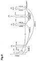
- the FFT operation and DBF synthesis illustrated in Fig. 6 are carried out in each of the up interval data and down interval data. After that, pairing is carried out between frequency peaks in the up interval and in the down interval to obtain information about the velocity, distance, and direction of the target object, based on the result thereof.
- Fig. 7 is a diagram to show the structure of the FM-CW radar apparatus as a second embodiment of the present invention.
- the FM-CW radar apparatus of the first embodiment is designed to effect the homodyne detection, whereas the radar apparatus of the present embodiment is designed to decrease the noise by carrying out the heterodyne detection.
- the changeover switch section 6 is composed of a switch body 61 and a switch control 62, similar to the changeover switch section 3 of Fig. 1.
- the switch body 61 has nine input terminals and one output terminal, and the output terminal is connected to either one of the input terminals.
- the connection of the output terminal is changed over at regular intervals according to a changeover signal from the switch control 62.
- the difference from the switch body 31 of the first embodiment is that the connection between the input terminals and the output terminal is interrupted by intermittent signals supplied from the outside.
- the switch control 62 is the same as that 32 of the first embodiment.
- the receiving circuit section 7 is constructed in such structure that an IF amplifier 71 and a second mixer 72 are interposed in series between the mixer 42 and the amplifier 43 of the receiving circuit section 4 of Fig. 1. Further, it has an oscillator 73 for outputting the intermittent signals f IF having the frequency equal to several ten times that of the changeover signal fsw.
- An example of the frequencies of the respective signals is as follows; the frequency f0 of the transmitted signal is, for example, 76 GHz, the frequency f IF of the intermittent signals in an intermediate frequency band is, for example, 100 MHz, the frequency of the changeover signal is, for example, 5 MHz, and the frequency of the beat signals is, for example, DC to 100 kHz.
- Fig. 8 is a spectral map to show the way of frequency conversion in the signal processing operation in the present embodiment.
- a received signal 130 is replaced with signals 131 and 132 by on/off according to the intermittent signals in the changeover switch section 6 and thereafter they are downconverted to an intermediate signal 133 in the mixer 42. Subsequent to it, the intermediate signal 133 is downconverted to a beat signal 134 in the second mixer 72.
- a curve 136 indicates a noise floor of the mixer 42 and a curve 136 a noise floor of the second mixer 72.
- the mixer 42 downconverts the signals into the IF zone where the influence of noise is low.
- the second mixer 72 having lower noise in the low frequency band than the mixer 42 downconverts the signal to the beat signal. Therefore, the present embodiment may expand the noise margin considerably, as compared with the homodyne method.
- the mixer 42 Since the mixer 42 has the very wide bandwidth, there normally appears a lot of 1/f noise and FM-AM conversion noise by the FM-CW method in the low frequency range. In contrast, since the second mixer 72 has the narrow bandwidth, the noise floor is lowered.
- the present embodiment achieves the expansion of noise margin by making use of such action.
- the IF signal may be separated from the FM-AM conversion noise appearing in the low frequency range, so that the low-frequency noise may be decreased further.
- the number of channels of the antenna elements was nine, but the detection accuracy may be enhanced further by increasing the number of channels.
- the FM-CW radar apparatus of the present invention needs only one set of the expensive devices necessary for the downconversion, for example, the RF amplifier, the high-frequency mixer, etc., regardless of the number of antenna elements. Therefore, the whole apparatus may be constructed at low cost and in compact size.
- the switch means connects only part of the antenna elements to the beat signal generating circuit in one period of the repetition periods of frequency modulation, so that the switching frequency may be lower than in the case wherein all the antenna elements are connected to the beat signal generating circuit in one period. Further taking it into consideration that a beat signal is sampled every changeover of connection, the A/D conversion rate may also be decreased with decrease in the switching frequency. This permits use of cheaper switch element and A/D converter.
Landscapes
- Engineering & Computer Science (AREA)
- Radar, Positioning & Navigation (AREA)
- Remote Sensing (AREA)
- Computer Networks & Wireless Communication (AREA)
- Physics & Mathematics (AREA)
- General Physics & Mathematics (AREA)
- Signal Processing (AREA)
- Radar Systems Or Details Thereof (AREA)
Applications Claiming Priority (3)
| Application Number | Priority Date | Filing Date | Title |
|---|---|---|---|
| JP11858498 | 1998-04-28 | ||
| JP11858498A JP3534164B2 (ja) | 1998-04-28 | 1998-04-28 | Fm−cwレーダ装置 |
| PCT/JP1999/001484 WO1999056147A1 (fr) | 1998-04-28 | 1999-03-24 | Radar a ondes continues modulees en frequence |
Publications (3)
| Publication Number | Publication Date |
|---|---|
| EP1076244A1 true EP1076244A1 (fr) | 2001-02-14 |
| EP1076244A4 EP1076244A4 (fr) | 2001-10-24 |
| EP1076244B1 EP1076244B1 (fr) | 2011-05-04 |
Family
ID=14740213
Family Applications (1)
| Application Number | Title | Priority Date | Filing Date |
|---|---|---|---|
| EP99910679A Expired - Lifetime EP1076244B1 (fr) | 1998-04-28 | 1999-03-24 | Radar a ondes continues modulees en frequence |
Country Status (9)
| Country | Link |
|---|---|
| US (1) | US6445339B1 (fr) |
| EP (1) | EP1076244B1 (fr) |
| JP (1) | JP3534164B2 (fr) |
| KR (1) | KR20010043118A (fr) |
| CN (1) | CN1206544C (fr) |
| AU (1) | AU744641B2 (fr) |
| CA (1) | CA2330430C (fr) |
| DE (1) | DE69943409D1 (fr) |
| WO (1) | WO1999056147A1 (fr) |
Cited By (2)
| Publication number | Priority date | Publication date | Assignee | Title |
|---|---|---|---|---|
| EP1464986A1 (fr) * | 2003-04-03 | 2004-10-06 | Fujitsu Ten Limited | Appareil radar |
| EP1760488A4 (fr) * | 2004-06-21 | 2007-08-15 | Fujitsu Ten Ltd | Appareil radar |
Families Citing this family (31)
| Publication number | Priority date | Publication date | Assignee | Title |
|---|---|---|---|---|
| EP1184678A3 (fr) | 2000-08-28 | 2003-01-29 | Stanley Electric Co., Ltd. | Transrépondeur pour radar |
| JP2002236170A (ja) * | 2001-02-06 | 2002-08-23 | Fujitsu Ten Ltd | Fm−cwレーダ処理装置 |
| JP3788322B2 (ja) * | 2001-05-30 | 2006-06-21 | 株式会社村田製作所 | レーダ |
| JP4067456B2 (ja) | 2003-06-09 | 2008-03-26 | 富士通テン株式会社 | レーダ装置及びその信号処理制御方法 |
| US7504990B2 (en) | 2004-01-15 | 2009-03-17 | Fujitsu Ten Limited | Radar apparatus |
| JP4120692B2 (ja) * | 2004-05-11 | 2008-07-16 | 株式会社村田製作所 | レーダ |
| JP4420743B2 (ja) * | 2004-05-31 | 2010-02-24 | 富士通テン株式会社 | Fm−cwレーダ装置 |
| JP2006003303A (ja) | 2004-06-21 | 2006-01-05 | Fujitsu Ten Ltd | レーダ装置 |
| JP2006010329A (ja) * | 2004-06-22 | 2006-01-12 | Fujitsu Ten Ltd | レーダのタイミング調整方法およびタイミング自動調整機能を有するレーダ装置 |
| US7439905B2 (en) * | 2004-09-13 | 2008-10-21 | Fujitsu Ten Limited | Radar apparatus |
| CN100414317C (zh) * | 2004-12-17 | 2008-08-27 | 电子科技大学 | 一种伪随机复合调制信号的非完全匹配处理方法 |
| JP4665590B2 (ja) * | 2005-03-31 | 2011-04-06 | 日本電気株式会社 | 干渉型レーダ |
| WO2006134912A1 (fr) * | 2005-06-17 | 2006-12-21 | Murata Manufacturing Co., Ltd. | Appareil radar |
| KR100751065B1 (ko) * | 2005-12-07 | 2007-08-22 | 한국전자통신연구원 | Rf 송수신 모듈 및 이를 이용한 밀리미터파 fmcw레이더 센서 |
| US7170440B1 (en) * | 2005-12-10 | 2007-01-30 | Landray Technology, Inc. | Linear FM radar |
| JP4602267B2 (ja) * | 2006-02-27 | 2010-12-22 | 株式会社デンソーアイティーラボラトリ | 電子走査式レーダ装置 |
| KR100750967B1 (ko) * | 2006-05-02 | 2007-08-22 | 한국전기연구원 | 가상 배열형 안테나 시스템 기반의 근거리 고해상도 차량용레이더 시스템 |
| KR100772927B1 (ko) * | 2006-09-29 | 2007-11-02 | 한국전자통신연구원 | 레이더 센서용 헤테로다인 rf 송수신기 |
| JP4737165B2 (ja) * | 2006-10-31 | 2011-07-27 | 株式会社村田製作所 | レーダの物標検知方法、およびこの物標検知方法を用いたレーダ装置 |
| US7755533B2 (en) * | 2006-11-01 | 2010-07-13 | Imsar Llc | Interferometric switched beam radar apparatus and method |
| JP4903094B2 (ja) * | 2007-07-19 | 2012-03-21 | 三菱電機株式会社 | レーダ装置 |
| JP5407272B2 (ja) * | 2008-06-12 | 2014-02-05 | 三菱電機株式会社 | レーダ装置 |
| JP5630034B2 (ja) * | 2010-03-04 | 2014-11-26 | 富士通株式会社 | レーダ装置及び目標探知方法 |
| JP5655516B2 (ja) * | 2010-11-12 | 2015-01-21 | 株式会社デンソー | レーダ装置 |
| KR101207718B1 (ko) * | 2011-03-15 | 2012-12-03 | 주식회사 만도 | 주파수변조연속파 레이더 시스템 |
| CN102928834B (zh) * | 2012-11-23 | 2014-05-14 | 北京理工大学 | 一种基于无相位突变拼接信号的调频连续波测距方法 |
| US9417315B2 (en) * | 2012-12-20 | 2016-08-16 | The Board Of Regents Of The University Of Oklahoma | Radar system and methods for making and using same |
| TWI464441B (zh) * | 2013-08-28 | 2014-12-11 | U & U Engineering Inc | 具有距離閘功能之微波偵測器 |
| EP3059559A1 (fr) * | 2015-02-23 | 2016-08-24 | Siemens Aktiengesellschaft | Système de radar FMCW |
| CN112534298A (zh) * | 2018-08-07 | 2021-03-19 | 株式会社村田制作所 | 雷达装置 |
| WO2020165952A1 (fr) * | 2019-02-12 | 2020-08-20 | 三菱電機株式会社 | Dispositif radar, procédé de détection d'objet à observer, et dispositif embarqué |
Family Cites Families (17)
| Publication number | Priority date | Publication date | Assignee | Title |
|---|---|---|---|---|
| US4107692A (en) | 1977-03-09 | 1978-08-15 | Raytheon Company | Radio frequency signal direction finding system |
| DE2751990A1 (de) | 1977-11-22 | 1979-05-23 | Storz Karl | Laryngoakop mit einer injektionsduese |
| US4150375A (en) | 1978-03-02 | 1979-04-17 | Sperry Rand Corporation | Interferometric protective system for vehicles |
| GB2249685A (en) | 1990-11-09 | 1992-05-13 | Philips Electronic Associated | Synchronizing a radar receiver |
| JPH04313091A (ja) * | 1991-04-10 | 1992-11-05 | Honda Motor Co Ltd | Fmレーダ装置 |
| US5389939A (en) | 1993-03-31 | 1995-02-14 | Hughes Aircraft Company | Ultra wideband phased array antenna |
| JP2989428B2 (ja) | 1993-06-17 | 1999-12-13 | 本田技研工業株式会社 | 時分割型fmレーダシステム |
| JPH07120547A (ja) | 1993-10-21 | 1995-05-12 | Honda Motor Co Ltd | レーダ装置 |
| JP3256374B2 (ja) | 1994-05-27 | 2002-02-12 | 本田技研工業株式会社 | マルチビーム・レーダ装置 |
| US5486832A (en) | 1994-07-01 | 1996-01-23 | Hughes Missile Systems Company | RF sensor and radar for automotive speed and collision avoidance applications |
| JP3300558B2 (ja) * | 1994-11-10 | 2002-07-08 | 本田技研工業株式会社 | 車載用マルチ・チャネルレーダー装置 |
| JP3491418B2 (ja) | 1995-12-01 | 2004-01-26 | 株式会社デンソー | Fmcwレーダ装置 |
| JP3460453B2 (ja) * | 1995-12-11 | 2003-10-27 | 株式会社デンソー | Fmcwレーダ装置 |
| US5933109A (en) | 1996-05-02 | 1999-08-03 | Honda Giken Kabushiki Kaisha | Multibeam radar system |
| JP3061261B2 (ja) * | 1997-04-01 | 2000-07-10 | 本田技研工業株式会社 | Fmレーダ装置 |
| JP3597678B2 (ja) | 1997-08-18 | 2004-12-08 | 富士通株式会社 | レーダ装置 |
| JP3525426B2 (ja) * | 1997-11-28 | 2004-05-10 | トヨタ自動車株式会社 | レーダ装置 |
-
1998
- 1998-04-28 JP JP11858498A patent/JP3534164B2/ja not_active Expired - Lifetime
-
1999
- 1999-03-24 DE DE69943409T patent/DE69943409D1/de not_active Expired - Lifetime
- 1999-03-24 CN CNB998055387A patent/CN1206544C/zh not_active Expired - Lifetime
- 1999-03-24 CA CA002330430A patent/CA2330430C/fr not_active Expired - Lifetime
- 1999-03-24 WO PCT/JP1999/001484 patent/WO1999056147A1/fr not_active Ceased
- 1999-03-24 KR KR1020007012009A patent/KR20010043118A/ko not_active Ceased
- 1999-03-24 EP EP99910679A patent/EP1076244B1/fr not_active Expired - Lifetime
- 1999-03-24 AU AU29572/99A patent/AU744641B2/en not_active Expired
-
2000
- 2000-10-30 US US09/698,018 patent/US6445339B1/en not_active Expired - Lifetime
Cited By (5)
| Publication number | Priority date | Publication date | Assignee | Title |
|---|---|---|---|---|
| EP1464986A1 (fr) * | 2003-04-03 | 2004-10-06 | Fujitsu Ten Limited | Appareil radar |
| US6859168B2 (en) | 2003-04-03 | 2005-02-22 | Fujitsu Ten Limited | Radar apparatus |
| EP1760488A4 (fr) * | 2004-06-21 | 2007-08-15 | Fujitsu Ten Ltd | Appareil radar |
| US7429947B2 (en) | 2004-06-21 | 2008-09-30 | Fujitsu Ten Limited | Radar apparatus for detecting distance or velocity with respect to an object |
| CN1898578B (zh) * | 2004-06-21 | 2010-06-09 | 富士通天株式会社 | 雷达装置 |
Also Published As
| Publication number | Publication date |
|---|---|
| AU744641B2 (en) | 2002-02-28 |
| CA2330430A1 (fr) | 1999-11-04 |
| KR20010043118A (ko) | 2001-05-25 |
| CA2330430C (fr) | 2004-06-08 |
| CN1298488A (zh) | 2001-06-06 |
| EP1076244B1 (fr) | 2011-05-04 |
| JPH11311668A (ja) | 1999-11-09 |
| AU2957299A (en) | 1999-11-16 |
| EP1076244A4 (fr) | 2001-10-24 |
| JP3534164B2 (ja) | 2004-06-07 |
| WO1999056147A1 (fr) | 1999-11-04 |
| DE69943409D1 (en) | 2011-06-16 |
| US6445339B1 (en) | 2002-09-03 |
| CN1206544C (zh) | 2005-06-15 |
Similar Documents
| Publication | Publication Date | Title |
|---|---|---|
| CA2330430C (fr) | Radar a ondes continues modulees en frequence | |
| JP3525426B2 (ja) | レーダ装置 | |
| EP0981059B1 (fr) | Système de radar à onde entretenue et modulée en fréquence | |
| CN100360955C (zh) | 雷达装置 | |
| US6067048A (en) | Radar apparatus | |
| US6121917A (en) | FM-CW radar | |
| JP3575694B2 (ja) | 走査型fmcwレーダ | |
| JP2000284047A (ja) | レーダ装置 | |
| US20120119940A1 (en) | Radar apparatus with multi-receiver channel | |
| JP3489114B2 (ja) | Fm−cwレーダ装置 | |
| US20060055593A1 (en) | Radar apparatus | |
| JP3366615B2 (ja) | パルスレーダ装置 | |
| JP3500629B2 (ja) | Dbfレーダ装置 | |
| JP3482870B2 (ja) | Fm−cwレーダ装置 | |
| RU2365935C1 (ru) | Устройство формирования и обработки сигналов для рлс с частотно-сканирующей антенной решеткой | |
| US12366652B2 (en) | Apparatus and method for controlling radar in vehicle | |
| JP2550504B2 (ja) | レーダ装置 | |
| JP2007225319A (ja) | パルスレーダ装置 | |
| JPH11271435A (ja) | モノパルス受信機 | |
| JP4238360B2 (ja) | 測距装置 |
Legal Events
| Date | Code | Title | Description |
|---|---|---|---|
| PUAI | Public reference made under article 153(3) epc to a published international application that has entered the european phase |
Free format text: ORIGINAL CODE: 0009012 |
|
| 17P | Request for examination filed |
Effective date: 20001026 |
|
| AK | Designated contracting states |
Kind code of ref document: A1 Designated state(s): DE FR GB NL SE |
|
| A4 | Supplementary search report drawn up and despatched |
Effective date: 20010906 |
|
| AK | Designated contracting states |
Kind code of ref document: A4 Designated state(s): DE FR GB NL SE |
|
| 17Q | First examination report despatched |
Effective date: 20080703 |
|
| GRAP | Despatch of communication of intention to grant a patent |
Free format text: ORIGINAL CODE: EPIDOSNIGR1 |
|
| GRAS | Grant fee paid |
Free format text: ORIGINAL CODE: EPIDOSNIGR3 |
|
| GRAA | (expected) grant |
Free format text: ORIGINAL CODE: 0009210 |
|
| AK | Designated contracting states |
Kind code of ref document: B1 Designated state(s): DE FR GB NL SE |
|
| REG | Reference to a national code |
Ref country code: GB Ref legal event code: FG4D |
|
| REF | Corresponds to: |
Ref document number: 69943409 Country of ref document: DE Date of ref document: 20110616 Kind code of ref document: P |
|
| REG | Reference to a national code |
Ref country code: DE Ref legal event code: R096 Ref document number: 69943409 Country of ref document: DE Effective date: 20110616 |
|
| REG | Reference to a national code |
Ref country code: SE Ref legal event code: TRGR |
|
| REG | Reference to a national code |
Ref country code: NL Ref legal event code: T3 |
|
| PLBE | No opposition filed within time limit |
Free format text: ORIGINAL CODE: 0009261 |
|
| STAA | Information on the status of an ep patent application or granted ep patent |
Free format text: STATUS: NO OPPOSITION FILED WITHIN TIME LIMIT |
|
| 26N | No opposition filed |
Effective date: 20120207 |
|
| REG | Reference to a national code |
Ref country code: DE Ref legal event code: R097 Ref document number: 69943409 Country of ref document: DE Effective date: 20120207 |
|
| REG | Reference to a national code |
Ref country code: GB Ref legal event code: 746 Effective date: 20121219 |
|
| REG | Reference to a national code |
Ref country code: DE Ref legal event code: R084 Ref document number: 69943409 Country of ref document: DE Effective date: 20121213 |
|
| REG | Reference to a national code |
Ref country code: FR Ref legal event code: PLFP Year of fee payment: 18 |
|
| REG | Reference to a national code |
Ref country code: FR Ref legal event code: PLFP Year of fee payment: 19 |
|
| REG | Reference to a national code |
Ref country code: FR Ref legal event code: PLFP Year of fee payment: 20 |
|
| PGFP | Annual fee paid to national office [announced via postgrant information from national office to epo] |
Ref country code: NL Payment date: 20180214 Year of fee payment: 20 |
|
| PGFP | Annual fee paid to national office [announced via postgrant information from national office to epo] |
Ref country code: DE Payment date: 20180313 Year of fee payment: 20 Ref country code: GB Payment date: 20180321 Year of fee payment: 20 |
|
| PGFP | Annual fee paid to national office [announced via postgrant information from national office to epo] |
Ref country code: FR Payment date: 20180223 Year of fee payment: 20 Ref country code: SE Payment date: 20180313 Year of fee payment: 20 |
|
| REG | Reference to a national code |
Ref country code: DE Ref legal event code: R071 Ref document number: 69943409 Country of ref document: DE |
|
| REG | Reference to a national code |
Ref country code: NL Ref legal event code: MK Effective date: 20190323 |
|
| REG | Reference to a national code |
Ref country code: GB Ref legal event code: PE20 Expiry date: 20190323 |
|
| PG25 | Lapsed in a contracting state [announced via postgrant information from national office to epo] |
Ref country code: GB Free format text: LAPSE BECAUSE OF EXPIRATION OF PROTECTION Effective date: 20190323 |