EP1085459A2 - Method of manufacturing card-type storage device and card-type storage device - Google Patents
Method of manufacturing card-type storage device and card-type storage device Download PDFInfo
- Publication number
- EP1085459A2 EP1085459A2 EP00101637A EP00101637A EP1085459A2 EP 1085459 A2 EP1085459 A2 EP 1085459A2 EP 00101637 A EP00101637 A EP 00101637A EP 00101637 A EP00101637 A EP 00101637A EP 1085459 A2 EP1085459 A2 EP 1085459A2
- Authority
- EP
- European Patent Office
- Prior art keywords
- frame member
- support frame
- memory module
- card
- image
- Prior art date
- Legal status (The legal status is an assumption and is not a legal conclusion. Google has not performed a legal analysis and makes no representation as to the accuracy of the status listed.)
- Withdrawn
Links
Images






Classifications
-
- G—PHYSICS
- G06—COMPUTING OR CALCULATING; COUNTING
- G06K—GRAPHICAL DATA READING; PRESENTATION OF DATA; RECORD CARRIERS; HANDLING RECORD CARRIERS
- G06K19/00—Record carriers for use with machines and with at least a part designed to carry digital markings
- G06K19/06—Record carriers for use with machines and with at least a part designed to carry digital markings characterised by the kind of the digital marking, e.g. shape, nature, code
- G06K19/067—Record carriers with conductive marks, printed circuits or semiconductor circuit elements, e.g. credit or identity cards also with resonating or responding marks without active components
- G06K19/07—Record carriers with conductive marks, printed circuits or semiconductor circuit elements, e.g. credit or identity cards also with resonating or responding marks without active components with integrated circuit chips
-
- G—PHYSICS
- G06—COMPUTING OR CALCULATING; COUNTING
- G06K—GRAPHICAL DATA READING; PRESENTATION OF DATA; RECORD CARRIERS; HANDLING RECORD CARRIERS
- G06K19/00—Record carriers for use with machines and with at least a part designed to carry digital markings
- G06K19/06—Record carriers for use with machines and with at least a part designed to carry digital markings characterised by the kind of the digital marking, e.g. shape, nature, code
- G06K19/067—Record carriers with conductive marks, printed circuits or semiconductor circuit elements, e.g. credit or identity cards also with resonating or responding marks without active components
- G06K19/07—Record carriers with conductive marks, printed circuits or semiconductor circuit elements, e.g. credit or identity cards also with resonating or responding marks without active components with integrated circuit chips
- G06K19/077—Constructional details, e.g. mounting of circuits in the carrier
- G06K19/07745—Mounting details of integrated circuit chips
-
- G—PHYSICS
- G06—COMPUTING OR CALCULATING; COUNTING
- G06K—GRAPHICAL DATA READING; PRESENTATION OF DATA; RECORD CARRIERS; HANDLING RECORD CARRIERS
- G06K19/00—Record carriers for use with machines and with at least a part designed to carry digital markings
- G06K19/06—Record carriers for use with machines and with at least a part designed to carry digital markings characterised by the kind of the digital marking, e.g. shape, nature, code
- G06K19/067—Record carriers with conductive marks, printed circuits or semiconductor circuit elements, e.g. credit or identity cards also with resonating or responding marks without active components
- G06K19/07—Record carriers with conductive marks, printed circuits or semiconductor circuit elements, e.g. credit or identity cards also with resonating or responding marks without active components with integrated circuit chips
- G06K19/077—Constructional details, e.g. mounting of circuits in the carrier
-
- Y—GENERAL TAGGING OF NEW TECHNOLOGICAL DEVELOPMENTS; GENERAL TAGGING OF CROSS-SECTIONAL TECHNOLOGIES SPANNING OVER SEVERAL SECTIONS OF THE IPC; TECHNICAL SUBJECTS COVERED BY FORMER USPC CROSS-REFERENCE ART COLLECTIONS [XRACs] AND DIGESTS
- Y10—TECHNICAL SUBJECTS COVERED BY FORMER USPC
- Y10T—TECHNICAL SUBJECTS COVERED BY FORMER US CLASSIFICATION
- Y10T29/00—Metal working
- Y10T29/49—Method of mechanical manufacture
- Y10T29/49002—Electrical device making
- Y10T29/49117—Conductor or circuit manufacturing
- Y10T29/49124—On flat or curved insulated base, e.g., printed circuit, etc.
- Y10T29/49126—Assembling bases
-
- Y—GENERAL TAGGING OF NEW TECHNOLOGICAL DEVELOPMENTS; GENERAL TAGGING OF CROSS-SECTIONAL TECHNOLOGIES SPANNING OVER SEVERAL SECTIONS OF THE IPC; TECHNICAL SUBJECTS COVERED BY FORMER USPC CROSS-REFERENCE ART COLLECTIONS [XRACs] AND DIGESTS
- Y10—TECHNICAL SUBJECTS COVERED BY FORMER USPC
- Y10T—TECHNICAL SUBJECTS COVERED BY FORMER US CLASSIFICATION
- Y10T29/00—Metal working
- Y10T29/49—Method of mechanical manufacture
- Y10T29/49002—Electrical device making
- Y10T29/49117—Conductor or circuit manufacturing
- Y10T29/49124—On flat or curved insulated base, e.g., printed circuit, etc.
- Y10T29/4913—Assembling to base an electrical component, e.g., capacitor, etc.
-
- Y—GENERAL TAGGING OF NEW TECHNOLOGICAL DEVELOPMENTS; GENERAL TAGGING OF CROSS-SECTIONAL TECHNOLOGIES SPANNING OVER SEVERAL SECTIONS OF THE IPC; TECHNICAL SUBJECTS COVERED BY FORMER USPC CROSS-REFERENCE ART COLLECTIONS [XRACs] AND DIGESTS
- Y10—TECHNICAL SUBJECTS COVERED BY FORMER USPC
- Y10T—TECHNICAL SUBJECTS COVERED BY FORMER US CLASSIFICATION
- Y10T29/00—Metal working
- Y10T29/49—Method of mechanical manufacture
- Y10T29/49002—Electrical device making
- Y10T29/49117—Conductor or circuit manufacturing
- Y10T29/49124—On flat or curved insulated base, e.g., printed circuit, etc.
- Y10T29/49155—Manufacturing circuit on or in base
-
- Y—GENERAL TAGGING OF NEW TECHNOLOGICAL DEVELOPMENTS; GENERAL TAGGING OF CROSS-SECTIONAL TECHNOLOGIES SPANNING OVER SEVERAL SECTIONS OF THE IPC; TECHNICAL SUBJECTS COVERED BY FORMER USPC CROSS-REFERENCE ART COLLECTIONS [XRACs] AND DIGESTS
- Y10—TECHNICAL SUBJECTS COVERED BY FORMER USPC
- Y10T—TECHNICAL SUBJECTS COVERED BY FORMER US CLASSIFICATION
- Y10T29/00—Metal working
- Y10T29/49—Method of mechanical manufacture
- Y10T29/49002—Electrical device making
- Y10T29/49117—Conductor or circuit manufacturing
- Y10T29/49169—Assembling electrical component directly to terminal or elongated conductor
- Y10T29/49171—Assembling electrical component directly to terminal or elongated conductor with encapsulating
- Y10T29/49172—Assembling electrical component directly to terminal or elongated conductor with encapsulating by molding of insulating material
-
- Y—GENERAL TAGGING OF NEW TECHNOLOGICAL DEVELOPMENTS; GENERAL TAGGING OF CROSS-SECTIONAL TECHNOLOGIES SPANNING OVER SEVERAL SECTIONS OF THE IPC; TECHNICAL SUBJECTS COVERED BY FORMER USPC CROSS-REFERENCE ART COLLECTIONS [XRACs] AND DIGESTS
- Y10—TECHNICAL SUBJECTS COVERED BY FORMER USPC
- Y10T—TECHNICAL SUBJECTS COVERED BY FORMER US CLASSIFICATION
- Y10T29/00—Metal working
- Y10T29/49—Method of mechanical manufacture
- Y10T29/49002—Electrical device making
- Y10T29/49117—Conductor or circuit manufacturing
- Y10T29/49174—Assembling terminal to elongated conductor
- Y10T29/49176—Assembling terminal to elongated conductor with molding of electrically insulating material
Definitions
- the present invention relates to a method of manufacturing a card-type storage device and a card-type storage device.
- the present invention relates to a technique for facilitating a manufacturing a frame that supports a semiconductor memory, and for enabling the storage device itself to indicate contents stored in the storage device, in a thin type card-type storage that incorporates a semiconductor memory.
- Figures 1 and 2 show the structure of a conventional standard card-type storage device, in which Fig. 1 is a perspective view and Fig. 2 a sectional view.
- a conventional technique for manufacturing such a card-type storage device injection-molds a card-type frame 111 of solid body from plastic.
- the frame 111 has an opening 111a to receive a memory module 113.
- the memory module 113 has a semiconductor memory 113a and a flat electrode 113b and is fitted into the opening 111a of the frame 111 to be fixed such that the flat electrode 113b is exposed.
- the frame 111 which is injection-molded into solid body, must have a very thin recessed bottom 111b under the opening 111a for receiving the memory module 113.
- a precision metal mold must be prepared through difficult processes, and the inside of the metal mold must be kept under a low pressure when injecting resin into it. This complicates the structure of a molding mechanism and makes the resin injection work difficult.
- the conventional technique is hardly capable of manufacturing thin, small card-type storage devices having a thin recessed bottom 111b.
- a card-type storage device with transparent or translucent material provides an advantage to show an image printed on the storage device to a user so that the user may easily recognize the contents of information stored therein, as a characteristic of above mentioned card-type storage device.
- the conventional technique allows only limited materials to form card-type frame 111 of solid body. Accordingly, the conventional, technique is unable to freely form transparent or translucent card-type storage devices to meet various applications for card-type frame thereof.
- An object of the present invention is to provide a method of manufacturing a small, thin card-type storage device, capable of easily manufacturing a frame for the storage device from a variety of resin materials without forming a very thin recessed bottom of the frame.
- Another object of the present invention is to provide a card-type storage device enabling the storage device to indicate contents stored therein.
- the present invention forms a card-type storage device frame with a sheet and a support frame member.
- the sheet and support frame member may be made of transparent or translucent material.
- one aspect of the present invention provides a method of manufacturing a card-type storage device, including the steps of (a) preparing a card-type support frame member having an opening, (a') preparing a sheet material, (b) cutting the sheet material into the size of the support frame member, to form a support sheet. (c) bonding the support sheet to a bottom surface of the support frame member, to form a frame, and (d) fitting a memory module to be fixed in the opening of the support frame member in the frame.
- the memory module has at least one semiconductor memory sealed therein on a first surface of the memory module and a flat external terminal exposed on a second surface of the memory module.
- the memory module is fitted in the opening of the support frame member in the frame such that the second surface thereof aligns with a top surface of the frame.
- Another aspect of the present invention provides a method of manufacturing a card-type storage device, including the steps of (aa) preparing a card-type support frame member having an opening, (aa') preparing a sheet material, (bb) bonding a bottom surface of the support frame member onto the sheet material, (cc) cutting the sheet material along the support frame member, to form a frame made of the support frame member and the cut sheet material serving as a support sheet attached to the bottom surface of the support frame member, and (dd) fitting a memory module to be fixed in the opening of the support frame member in the frame.
- the memory module has at least one semiconductor memory sealed therein on a first surface of the memory module and a flat external terminal exposed on a second surface of the memory module.
- Another aspect of the present invention provides a method of manufacturing card-type storage devices, including the steps of (aaa) preparing, from resin, a frame member set made of consecutively joined card-type support frame members each having an opening, as well as a sheet material whose size is substantially equal to or larger than the frame member set; (bbb) bonding a bottom surface of the frame member set onto the sheet material, (ccc) cutting the frame set along the support frame members to simultaneously form frames each made of the support frame member and the cut sheet material serving as a support sheet attached to the bottom surface of the support frame member, and (ddd) fitting a memory module to be fixed in the opening of the support frame member of each of the frames.
- the memory module has at least one semiconductor memory sealed with resin on a first surface of the memory module and a flat external terminal exposed on a second surface of the memory module.
- Another aspect of the present invention provides a method of manufacturing a card-type storage device, including a card-type support frame member made of resin and having an opening, a support sheet bonded to a bottom surface of the support frame member, and a memory module having at least one semiconductor memory sealed with resin on a first surface of the memory module and a flat external terminal exposed on a second surface of the memory module.
- the method includes the steps of (a) preparing the support frame member and a sheet material, (b) cutting the sheet material into the size of the support frame member, to form the support sheet, (c) bonding the support sheet to the bottom surface of the support frame member, to form a frame, and (d) fitting the memory module to be fixed in the opening of the support frame member in the frame.
- the card-type storage device is manufactured by the steps of (a'') preparing the support frame member and a sheet material, (b'') cutting the sheet material into the size of the support frame member, to form the support sheet, (c'') bonding the support sheet to the bottom surface of the support frame member, to form a frame, and (d'') fitting the memory module to be fixed in the opening of the support frame member in the frame.
- a card-type storage device having (a) a frame and (b) a memory module.
- the frame includes a card-type support frame member having an opening and made of resin, and a support sheet bonded to a bottom surface of the support frame member.
- the support frame member bottomed with the support sheet forms the frame.
- the memory module includes at least one semiconductor memory sealed therein on a first surface of the memory module and a flat external terminal exposed on a second surface of the memory module.
- Figure 3 is a perspective view showing a card-type storage device manufactured according to the first embodiment of the present invention and Fig. 4 is a sectional view taken along a line IV-IV of Fig. 3.
- Fig. 5 shows a first surface of a memory module installed in the storage device of Figs. 3 and 4.
- This storage device is a so-called "SmartMedia” (that is registered trademark), which is a small, thin card-type storage device.
- the storage device comprises the memory module 13 of about, for example, 0.665 mm thick and a card-type frame 10 of about 0.76 mm ⁇ 0.08 mm thick.
- the frame 10 comprises a card-type support frame member 11 made of resin having an opening 11a, and a support sheet 12 bonded to a bottom surface of the support frame member 11.
- the opening 11a consists of a recess 11b and a through hole 11c that is formed at the bottom of the recess 11b and is smaller than the recess 11b. Making the through hole 11c smaller than the recess 11b is to firmly fit a semiconductor memory 13b of the memory module 13 to be fixed in the opening 11a.
- the support frame member 11 has a write-protect area 11d for prohibiting data in the memory 13b from being rewritten, and a label area 11e.
- the memory module 13 has a circuit board 13a having first and second surfaces.
- the semiconductor memory 13b is sealed with resin on the first surface of the circuit board 13a.
- Each connection terminal of the semiconductor memory 13b is connected to a wire 13e, which is connected to a through hole 13d.
- the through hole 13d is connected to a flat external terminal 13c, which is arranged on the second surface of the circuit board 13a.
- the memory module 13 is fitted to the support frame 11 such that the second surface of the memory module 13 aligns with a top surface of the support frame member 11.
- the memory module 13 fits to be fixed in the opening 11a of the frame 10 such that the flat external terminal 13c is exposed. More precisely, as shown in Fig. 4, the circuit board 13a is engaged in the recess 11b of the opening 11a, and the terminal 13c is flash with and exposed from the top surface of the frame 10. At the same time, the semiconductor memory 13b fits to be fixed in the through hole 11c. Namely, the recess 11b and through hole 11c of the opening 11a form a stepped structure to properly bold the semiconductor memory 13b and the terminal 13c of the memory module 13.
- the semiconductor memory 13b is, for example, a flash memory or a mask ROM.
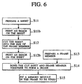
- Figure 6 is a process diagram generally showing the manufacturing method of the first embodiment.
- Figs. 7 to 11 show manufacturing steps according to the first embodiment.
- Figure 8 is a perspective view showing the card-type support frame member 11 and
- Fig. 9 is a sectional view taken along a line IX-IX of Fig. 8.
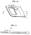
- Figure 10 is a perspective view showing the card-type frame 10 and Fig. 11 is a sectional view taken along a line XI -XI of Fig. 10.
- Step S11 prepares a sheet material of 0.10 mm to 0.17 mm thick.
- Step S12 cuts the sheet material into the size of the card-type support frame member 11, to form a support sheet 12 shown in Fig. 7, for example.
- step S13 prepares the support frame member 11 having the opening 11a by, for example, injection molding as shown in Figs. 8 and 9.
- the thickness of the support frame member 11 is, for example, about 0.665 mm, which is the same as the thickness of the memory module 13.
- Step S14 bonds the support sheet 12 to a bottom surface of the support frame member 11 with the use of adhesive agent, for example, to form the card-type frame 10 as shown in Figs. 10 and 11.
- adhesive agent for example, to form the card-type frame 10 as shown in Figs. 10 and 11.
- the bottom of the opening 11a of the support frame member 11 is closed with the support sheet 12. It is necessary to precisely align the support sheet 12 with the support frame member 11.
- the last step S15 fixes the memory module 13 in the opening 11a of the frame 10 with the use of, for example, adhesive agent, thereby completing the card-type storage device shown in Fig. 3.
- the recess bottom 111b should be formed (Fig. 2) to 0.13 mm to 0.15 mm. Therefor, it is nearly impossible for the conventional technique to form the card-type supporter having such a thin recess bottom by injection molding from transparent or translucent material with respect to the above "SmartMedia”.
- the manufacturing method of the first embodiment is capable of forming a small, thin card-type frame 10 without molding a very thin part of 0.2 mm thick or thinner from resin material even with small and thin card-type storage device such as "SmartMedia".
- the frame 10 of the first embodiment is manufacturable with the use of existing metal molds and injection molding machines.
- the frame 10 of the first embodiment is easily molded from an extended range of resin materials including transparent and translucent resin materials.
- the support frame member 11 and support sheet 12 that form the frame 10 may easily be formed to be transparent or translucent.
- an image that indicates and displays contents stored in the memory module 13 may be printed on the frame 10, so that a user may easily recognize the contents stored in the card-type storage device.
- the first embodiment enables a card-type storage device to have an indication of contents stored in the storage device.
- the indication may be an image representing contents such as music, book text, images, or voice reading a book.
- Such an image is, for example, a photograph or picture of a singer who sings the music stored in the storage device in computer readable electronic format.
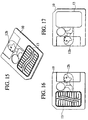
- Fig. 15 is a perspective view showing a picture 12b of a singer.
- Fig. 16 is a front view of Fig. 15, as well as Fig. 17 is a back view of Fig. 15.
- the indication may be other than images.
- the indication may be characters or letters. Such characters may be a code that uniquely identifies a particular music album by a particular singer or a particular book by a particular writer. Further, such characters may be just a title of a particular book.
- the support frame member 11 and support sheet 12 may be made from polycarbonate.
- the polycarbonate frame member 11 and sheet 12 hardly warp when they are bonded together into the frame 10, so that the frame 10 may be flat.
- One of the support frame member 11 and support sheet 12 may be made of polycarbonate, and the other polyester. This structure enables an image to firmly be printed on the frame 10.
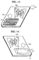
- step S12 of Fig. 6 After a transparent or translucent sheet is cut into the support sheet 12 in step S12 of Fig. 6, an image 12a of, for example, Fig. 14 is printed on the support sheet 12 in step S12b. Thereafter, steps S13, S14, and S15 are successively carried out to complete the transparent or translucent frame 10.
- a user can see the image 12a through the transparent or translucent frame 10 as shown in a top perspective view of Fig. 13 and a bottom perspective view of Fig. 14.
- the image 12a is printed on the support sheet 12, and then, the support sheet 12 is bonded to the support frame member 11 to form the frame 10. This improves the value of the card-type storage device serving as a package medium, that is a package marketed with contents.
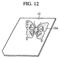
- step S12b instead of printing an image on the support sheet 12 in step S12b, an image may be printed on a sheet material that is not out yet, in step S11b. Namely, step S11b prints the image 12a of Fig. 12 on the sheet material prepared in step S11 in a surface area where the support frame member 11 is to be bonded, and thereafter, step S12 cuts the sheet material into the support sheet 12.
- the image 12a may be preferably printed on the surface of the support sheet 12 that is to be bonded to the support frame member 11, so that the image 12a may withstand abrasion.
- the surface of the support sheet 12 on which the image 12a is printed may be coated with a thin film to prevent adhesive agent from deteriorating or erasing the image 12a.
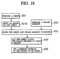
- Figures 18 to 19C show a method of manufacturing a card-type storage device according to the second embodiment of the present invention. The difference of the second embodiment from the first embodiment will be explained.
- Figure 18 is a process diagram generally showing the manufacturing method of the second embodiment, and Figs. 19A to 19C explain manufacturing processes of the second embodiment.
- Step S21 prepares a sheet material 12A of 0.10 mm to 0.17 mm thick as shown in Fig. 19A.
- the size of the sheet material 12A is larger than the support frame member 11.
- Step S22 prepares the support frame member 11, which is the same as that of Figs. 8 and 9.
- Step S23 bonds a bottom surface of the support frame member 11 onto the sheet material 12A as shown in Fig. 19B.
- Step S24 cuts the sheet material 12A along the support frame member 11 as shown in Fig. 19C, to complete a card-type frame 10 like the one shown in Figs. 10 and 11.
- the last step S25 fits a memory module 13 to be fixed in an opening 11a of the support frame member 11 with the use of, for example, adhesive agent, to complete a card-type storage device like the one shown in Fig. 3.
- the second embodiment prepares the large sheet material 12A, bonds the card-type support frame member 11 onto the sheet material 12A, and cuts the sheet material 12A along the support frame member 11.
- the second embodiment requires no precision when attaching the support frame member 11 to the sheet material 12A, thereby making the manufacturing of a card-type storage device easier.
- step S21 prepares the sheet material 12A first, and step S21b prints the image 12a in an area of the sheet material 12A where the support frame member 11 is to be bonded. Thereafter, step S23 bonds the support frame member 11 and sheet material 12A together, and step S24 cuts the sheet material 12A along the support frame member 11.
- the image 12a is preferable to print the image 12a on the surface area of the sheet material 12A that is to be bonded to the support frame member 11 and to coat the image-printed surface of the sheet material 12A with a thin film, to realize the effects of the first embodiment (Figs. 13 and 14).
- Figures 20 to 24 show a method of manufacturing a card-type storage device according to the third embodiment of the present invention. The difference of the third embodiment from the first and second embodiment will be explained.
- Figure 20 is a process diagram generally showing the manufacturing method of the third embodiment, and Figs. 21 to 24 explain manufacturing processes of the third embodiment.
- Step S31 prepares, from resin, a frame member set made of consecutively joined card-type support frame members 11 as shown in Fig. 21. Each boundary between the adjacent frame members 11 is provided with a tapered cut 11f as shown in Fig. 22.
- step S32 prepares a sheet material 12A whose size corresponds to the frame member set.
- the tapered cuts 11f make the following cut process easier, reduce stress on the support frame members 11, and provide smooth cut edges.
- the size of the sheet material 12A is substantially equal to or slightly larger than the size of the frame member set.
- Step S33 bonds a bottom surface of the frame member set onto the sheet material 12A as shown in Figs. 23 and 24.
- Step S34 uses the cuts 11f as guides to cut and separate the support frame members 11 and sheet material 12A from one another with the use of a metal mold, to simultaneously form card-type frames 10 each consisting of the support frame member 11 and a support sheet 12 attaching to the bottom of the support frame member 11.
- the last step S35 fits a memory module 13 to be fixed in an opening 11a of the support frame member 11 of each of the frames 10 with the use of, for example, adhesive agent, thereby simultaneously providing card-type storage devices each having the structure of Figs. 3 and 4.
- the third embodiment prepares a frame member set consisting of card-type support frame members 11 from resin, bonds the frame member set onto a sheet material 12A, and simultaneously cuts the frame member set and sheet material into card-type frames. Consequently, the third embodiment simultaneously produces card-type storage devices each having the structure of Figs. 3 and 4, to make the manufacturing of card-type storage devices easier and manufacturing costs lower compared with the first and second embodiments.
- step S32 prepares a sheet material 12A, and step S32b prints the image 12a in each area of the sheet material 12A where each frame member 11 is to be fixed. Thereafter, step S33 bonds a frame member set and the sheet material 12A together, and step S34 separates support frame members 11 from one another.
- the images 12a on the surface of the sheet material 12A to be bonded to the frame member set and to coat the image-printed surface of the sheet material 12A with a thin film, to realize the effects of the first embodiment (Figs. 13 and 14).
- the thickness of the card-type support frame member 11 is equal to the thickness (0.665 mm) of the memory module 13.
- the thickness of the support frame member 11 may be thicker than the memory module 13 by about 0.01 mm to 0.10 mm. In this case, there will be a gap between the semiconductor memory 13b and the support sheet 12. The gap may relax warping force applied to the card-type storage device, to prevent a breakage of the memory module 13.
- the image 12a is printed on the support sheet 12 so that the image 12a may not overlap the write-protect area 11d of the support frame member 11 when the support frame member 11 and support sheet 12 are bonded together.
- the write-protect area 11d is an area where a write-protect conductive seal is attached to prohibit data stored in the semiconductor memory 13b from erroneously being rewritten.
- the conductive seal is made of adhesive paper coated with aluminum or stainless steel.
- the support frame member 11 is made of nonconductive material, and therefore, two electrodes are brought in contact with the write-protect area 11d to check the conductivity of a signal applied between the two electrodes and determine whether or not it is write-protected.
- the area 11d may partly hide the image 12a when attaching the conductive seal to the write-protect area 11d. Although partly hiding the image 12a causes no electrical or functional problem, it is not preferable in terms of appearance. Accordingly, it is preferable to estimate and avoid the write-protect area 11d when printing an image on the support sheet 12. Namely, it is preferable to separate the image 12a from the write-protect area 11d.
- a card-type support frame member and a support sheet are separately prepared and are bonded together.
- the support frame member and sheet may be made of different materials and may have different colors.
- the support frame member may be white and the support sheet red, to form a two-color card-type storage device.
- This technique enables users to distinguish card-type storage devices, which have the same dimensions and shapes and different functions, from one another.
- card-type storage devices there are high-function storage devices that store individual identification (ID) data. Such high-function storage devices may be made in two-color structures, and low-function cards having no identification data in single-color structures, so that users may easily distinguish them from others.
- card-type storage devices incorporating flash memories that are electrically programmable may be made in two-color structures
- card-type storage devices incorporating mask ROMs that are read-only may be made in single-color structures.
- the support frame member When providing a card-type support frame member and a support sheet with different colors, at least the support frame member may be transparent or translucent so that a user may see an image printed on the support sheet through the support frame member.
- the image may indicate contents to be stored in the storage device, so that the storage device itself may display identification data for the contents thereof. Unlike printing an image on a label and attaching the label to the storage device, the image serving as contents identification data printed on the storage device thereof is hardly deteriorated or erased.
- the present invention cuts a sheet material into the size of a card-type support frame member and bonds the cut sheet to a bottom surface of the support frame member, to form a frame for a card-type storage device.
- the frame involves no thin part to be molded from resin, and therefore, is applicable even to form a so-called "SmartMedia” that is very small and thin.
- the supporter of the present invention is easy to manufacture from an extended range of resin materials with the use of existing metal molds and injecting machines.
- the present invention prepares a sheet material larger than a card-type support frame member, bonds a bottom surface of the support frame member onto the sheet material, and then cuts the sheet material along the support frame member to form a frame.
- This frame provides the same effect as the above-mentioned frame. This technique eliminates a precise alignment between the sheet and the support frame member, to make the manufacturing of a card-type storage device easier.
- the present invention prepares a frame member set consisting of consecutively joined card-type support frame members, bonds a bottom surface of the frame member set onto a sheet material, and then cuts the sheet-bonded frame member set along each of the support frame members, to simultaneously produce a plurality frames.
- this technique simultaneously manufactures a plurality of card-type storage devices to make the manufacturing of card-type storage devices easier and reduce the manufacturing costs of the storage devices.
- the present invention extends a range of resin materials to manufacture card-type storage devices. Namely, the present invention enables transparent and translucent resin materials to be used for manufacturing support frame members and sheets to form transparent and translucent card-type storage devices.
- an image may be printed on a support sheet that forms a transparent or translucent frame of a card-type storage device, so that the image may be seen through the frame. This improves the value of the card-type storage device when marketed as a package medium.
- the image-printed surface of the support sheet may be coated with a film so that the image may not be deteriorated or erased due to, for example, adhesive agent.
Landscapes
- Engineering & Computer Science (AREA)
- Computer Hardware Design (AREA)
- Microelectronics & Electronic Packaging (AREA)
- Physics & Mathematics (AREA)
- General Physics & Mathematics (AREA)
- Theoretical Computer Science (AREA)
- Credit Cards Or The Like (AREA)
Abstract
Description
Claims (55)
- A method of manufacturing a card-type storage device, comprising the steps of:(a) preparing a card-type support frame member (11) having an opening (11a) (S13);(a') preparing a sheet material (S11);(b) cutting the sheet material into the size of the support frame member (11), to form a support sheet (12) (S12);(c) bonding the support sheet (12) to a bottom surface of the support frame member (11), to form a frame (10) (S14); and(d) fitting a memory module (13) to be fixed in the opening (11a) of the support frame member (11) in the frame (10), the memory module (13) having at least one semiconductor memory (13b) sealed therein on a first surface of the memory module (13) and a flat external terminal exposed on a second surface of the memory module (13) (S15).
- The method of claim 1, further comprising the step of:(e) printing an image (12a) on the sheet material prepared at the step (a') in a surface area to be bonded to the support frame member (11) to form an image-printed surface (S11b), the step (a) being carried out before the step (b).
- The method of claim 2, wherein the image-printed surface of the support sheet (12) is bonded to the bottom of the support frame member (11), to form the frame (10) in the step (c).
- The method of claim 2, further comprising the step of:(f) coating the image-printed surface area with a transparent or translucent film, the step (f) being carried out before the step (b).
- The method of claim 1, further comprising the step of:(g) printing an image (12a) on the support sheet (12) cut at the step (b) to form an image-printed surface (S12b), the step (g) being carried out before the step (c).
- The method of claim 5, wherein the image-printed surface of the support sheet (12) is bonded to the bottom of the support frame member (11), to form the frame (10) in the step (c).
- The method of claim 5, further comprising the step of:(h) coating the image-printed surface area with a transparent or translucent film, the step (h) being carried out before the step (b).
- The method of claim 5, wherein the support frame member (11) prepared at the step (a) has a write-protect area (11d) adapted for being applied a write-protect seal indicating that writing data into the semiconductor memory (13b) is prohibited.
- The method of claim 8, wherein, in the step (e), the image (12a) is printed on an area other than the write-protect area (11d).
- The method of claim 8, wherein the step (a) affixes the write-protect seal to the write-protect area (11d).
- The method of claim 6, further comprising the step of:(h) coating the image-printed surface area with a transparent or translucent film, the step (h) being carried out before the step (c).
- The method of claim 1, wherein the opening (11a) is provided with a stepped area to hold the semiconductor memory (13b) and the flat external terminal of the memory module (13), respectively.
- The method of claim 1, wherein at least one of the support frame member (11) and sheet material is made from transparent or translucent material.
- The method of claim 13, wherein the support frame member (11) and sheet material are made from materials including at least one of polycarbonate and polyester.
- The method of claim 13, further comprising the step of:(e1) printing an image (12a) on the sheet material prepared at the step (a') in a surface area to be bonded to the support frame member (11), so that the image may indicate information stored in the memory module (13).
- The method of claim 2, wherein the support frame member (11) prepared at the step (a) has a write-protect area (11d) adapted for being applied a write-protect seal indicating that writing data into the semiconductor memory (13b) is prohibited.
- The method of claim 16, wherein, in the step (e), the image (12a) is printed on an area other than the write-protect area (11d).
- The method of claim 16, wherein the step (a) affixes the write-protect seal to the write-protect area (11d).
- A method of manufacturing a card-type storage device, comprising the steps of:(aa) preparing a card-type support frame member (11) having an opening (11a) (S22);(aa') preparing a sheet material (12A) (S21);(bb) bonding a bottom surface of the support frame member (11) onto the sheet material (12A) (S23);(cc) cutting the sheet material (12A) along the support frame member (11), to form a frame (10) made of the support frame member (11) and the cut sheet material (12) serving as a support sheet attached to the bottom surface of the support frame member (11) (S24); and(dd) fitting a memory module (13) to be fixed in the opening (11a) of the support frame member (11) in the frame (10) (S25), the memory module (13) having at least one semiconductor memory (13b) sealed therein on a first surface of the memory module (13) and a flat external terminal exposed on a second surface of the memory module (13).
- The method of claim 19, further comprising the step of:(ee) printing an image on the sheet material (12A) prepared at the step (aa') in a surface area to be bonded to the support frame member (11) (S21b), the step (ee) being carried out before the step (bb).
- The method of claim 20, wherein the bottom surface of the support frame member (11) is bonded onto the image-printed surface of the sheet material (12A) in the step (bb).
- The method of claim 20, further comprising the step of:(ff) coating the image-printed surface area with a transparent or translucent film, the step (ff) being carried out before the step (bb).
- The method of claim 19, wherein the opening 11a is provided with a stepped area to hold the semiconductor memory (13b) and the flat external terminal of the memory module (13), respectively.
- The method of claim 19, wherein at least one of the support frame member (11) and sheet material (12A) is made from transparent or translucent material.
- The method of claim 24, wherein the support frame member (11) and sheet material (12A) are made from materials including at least one of polycarbonate and polyester.
- The method of claim 19, further comprising the step of:(ee1) printing an image (12a) on the sheet material (12A) prepared at the step (aa') in a surface area to be bonded to the support frame member (11) (S21b), so that the image may indicate information stored in the memory module (13).
- The method of claim 20, wherein the support frame member (11) prepared at the step (aa) has a write-protect area (11d) adapted for being applied a write-protect seal indicating that writing data into the semiconductor memory (13b) is prohibited.
- The method of claim 27, wherein, in the step (ee), the image (12a) is printed on an area other than the write-protect area (11d).
- The method of claim 27, wherein the step (aa) affixes the write-protect seal to the write-protect area (11d).
- A method of manufacturing card-type storage devices, comprising the steps of:(aaa) preparing, from resin, a frame member set made of consecutively joined card-type support frame members (11) each having an opening (11a) (S31);(aaa') preparing a sheet material (12A) whose size is substantially equal to or larger than the frame member set (S32);(bbb) bonding a bottom surface of the frame member set onto the sheet material (12A) (S33);(ccc) cutting the frame member set along the support frame members (11) to simultaneously form frames (10) each made of the support frame member (11) and the cut sheet material serving as a support sheet (12) attached to the bottom surface of the support frame member (11) (S34); and(ddd) fitting a memory module (13) to be fixed in the opening (11a) of the support frame member (11) of each of the frames (10) (S35), the memory module (13) having at least one semiconductor memory (13b) sealed therein on a first surface of the memory module (13) and a flat external terminal, exposed on a second surface of the memory module (13).
- The method of claim 30, further comprising the step of:(eee) printing an image on the sheet material (12A) prepared at the step (aaa') in each surface area to be bonded to each support frame member (11) of the frame member set to form an image-printed surface (S32b), the step (eee) being carried out before the step (bbb).
- The method of claim 31, wherein the bottom surface of the frame member set is bonded onto the image-printed surface of the sheet material (12A) in the step (bbb).
- The method of claim 31, further comprising the step of:(fff) coating the image-printed surface with a transparent or translucent film, the step (fff) being carried out before the step (bbb).
- The method of claim 30, wherein the opening (11a) is provided with a stepped area to hold the semiconductor memory (13b) and the flat external terminal-of the memory module (13), respectively.
- The method of claim 30, wherein at least one of the frame member set and sheet material (12A) is made from transparent or translucent material.
- The method of claim 35, wherein the frame member set and sheet material (12A) are made from materials including at least one of polycarbonate and polyester.
- The method of claim 30, further comprising the step of:(eee1) printing an image on the sheet material (12A) prepared at the step (aaa') in each area to be bonded to each support frame member (11) of the frame member set (S32), so that the image may indicate information stored in each memory module (13).
- The method of claim 31, wherein each support frame (11) in the frame member set prepared at the step (aaa) has a write-protect area (11d) adapted for being applied a write-protect seal indicating that writing data into the semiconductor memory (13b) is prohibited.
- The method of claim 38, wherein, the step (eee), the image is printed on an area other than the write-protect area (11d).
- The method of claim 39, wherein the step (aaa) affixes the write-protect seal to each write-protect area (11d).
- A method of manufacturing a card-type storage device, including a card-type support frame member (11) made of resin and having an opening (11a), a support sheet (12) bonded to a bottom surface of the support frame member (11), and a memory module (13) having at least one semiconductor memory (13b) sealed with resin on a first surface of the memory module (13) and a flat external terminal exposed on a second surface of the memory module (13), comprising the steps of:(a) preparing the support frame member (11) and a sheet material (S13,S11);(b) cutting the sheet material into the site of the support frame member (11), to form the support sheet (12) (S12);(c) bonding the support sheet (12) to the bottom surface of the support frame member (11), to form a frame (10) (S14); and(d) fitting the memory module (13) to be fixed in the opening of the support frame member (11) in the frame (10) (S15).
- A card-type storage device, produced according to the process of claim 1.
- A card-type storage device, produced according to the process of claim 19.
- A card-type storage device, produced according to the process claim 30.
- A card-type storage device, comprising: a card-type support frame member (11) having an opening (11a) and made of transparent or translucent material;a support sheet (12) bonded to a bottom surface of the support frame member (11); anda memory module (13) having at least one semiconductor memory (13b) sealed therein on a first surface of the memory module (13) and a flat external terminal exposed on a second surface of the memory module (13), the card-type storage device being manufactured through the steps of:(a'') preparing the support frame member (11) and a sheet material (S11,S13);(b'') cutting the sheet material into the size of the support frame member (11), to form the support sheet (12) (S12);(c'') bonding the support sheet (12) to the bottom surface of the support frame member (11), to form a frame (10) (S14); and(d'') fitting the memory module (13) to be fixed in the opening (11a) of the support frame member (11) in theframe (10) (S15).
- A card-type storage device, comprising:(a) a frame (10) including, a card-type support frame member (11) having an opening (11a) and made of resin, and a support sheet (12) bonded to a bottom surface of the support frame member (11); and(b) a memory module (13) including at least one semiconductor memory (13b) sealed therein on a first surface of the memory module (13) and a flat external terminal exposed on a second surface of the memory module (13), the memory module (13) being fitted in the opening (11a) of the support frame member (11) in the frame such that the second surface thereof aligns with a top surface of the frame (11).
- The device of claim 46, wherein the support shoot (12) has an image printed on the surface thereof bonded to the support frame member (11).
- The device of claim 47, wherein at least one of the support frame member (11) and support sheet (12) is made from transparent or translucent material.
- The device of claim 47, wherein the support frame member (11) has a write-protect area (11d) separately from an area where the image (12a) printed on the support sheet (12) is present.
- The device of claim 46, wherein the opening (11a) is provided with a stepped area to hold the semiconductor memory (13b) and the flat external terminal of the memory module (13), respectively.
- The device of claim 46, wherein at least one of the support frame member (11) and support sheet (12) is made from transparent or translucent material.
- The device of claim 51, wherein the support frame member (11) and support sheet (12) are made from materials including at least one of polycarbonate and polyester.
- The device of claim 46, wherein the frame is one of a plurality of frames that are simultaneously produced.
- A card-type storage device, comprising:a card-type support frame member (11) including a first area and a second area, the first area having an opening (11a) and at least a portion of the second area being made from transparent or translucent material; anda memory module (13) fitted in the opening (11a), the memory module (13) including at least non-volatile semiconductor memory (13b), wherein said semiconductor memory (13b) contains certain information, and the second area has a picture or characters concerning said information.
- The device of claim 54, wherein said information is digitized music information, and said picture indicates a singer or a player of the music.
Applications Claiming Priority (2)
| Application Number | Priority Date | Filing Date | Title |
|---|---|---|---|
| JP26272499 | 1999-09-16 | ||
| JP26272499A JP2001084347A (en) | 1999-09-16 | 1999-09-16 | Card type storage device and method of manufacturing the same |
Publications (2)
| Publication Number | Publication Date |
|---|---|
| EP1085459A2 true EP1085459A2 (en) | 2001-03-21 |
| EP1085459A3 EP1085459A3 (en) | 2002-03-20 |
Family
ID=17379722
Family Applications (1)
| Application Number | Title | Priority Date | Filing Date |
|---|---|---|---|
| EP00101637A Withdrawn EP1085459A3 (en) | 1999-09-16 | 2000-01-31 | Method of manufacturing card-type storage device and card-type storage device |
Country Status (6)
| Country | Link |
|---|---|
| US (3) | US6295221B1 (en) |
| EP (1) | EP1085459A3 (en) |
| JP (1) | JP2001084347A (en) |
| KR (1) | KR100398855B1 (en) |
| CN (1) | CN1245757C (en) |
| TW (1) | TW456007B (en) |
Cited By (2)
| Publication number | Priority date | Publication date | Assignee | Title |
|---|---|---|---|---|
| WO2004034320A1 (en) * | 2002-10-11 | 2004-04-22 | Nagraid Sa | Electronic module comprising an element exposed on one surface and method for making same |
| US8316535B2 (en) | 2002-10-11 | 2012-11-27 | Nagraid Sa | Electronic device comprising a visible electronic element connected to an internal module and manufacturing process of such a device |
Families Citing this family (16)
| Publication number | Priority date | Publication date | Assignee | Title |
|---|---|---|---|---|
| US6001672A (en) * | 1997-02-25 | 1999-12-14 | Micron Technology, Inc. | Method for transfer molding encapsulation of a semiconductor die with attached heat sink |
| JP4470242B2 (en) * | 1999-04-23 | 2010-06-02 | ソニー株式会社 | Semiconductor memory card |
| JP2001084347A (en) * | 1999-09-16 | 2001-03-30 | Toshiba Corp | Card type storage device and method of manufacturing the same |
| US7174628B1 (en) * | 2005-03-03 | 2007-02-13 | Super Talent Electronics, Inc. | Memory card production using prefabricated cover and molded casing portion |
| US7220615B2 (en) * | 2001-06-11 | 2007-05-22 | Micron Technology, Inc. | Alternative method used to package multimedia card by transfer molding |
| JP3928522B2 (en) * | 2002-08-27 | 2007-06-13 | 株式会社村田製作所 | Card structure |
| JP2004246866A (en) * | 2003-01-21 | 2004-09-02 | Toshiba Corp | Storage device, data etc. writing device and writing method |
| USD509243S1 (en) * | 2003-05-22 | 2005-09-06 | Mastercard International Incorporated | Card |
| USD511355S1 (en) * | 2004-04-08 | 2005-11-08 | Mastercard International Incorporated | Card with notch |
| TWM282293U (en) * | 2005-07-22 | 2005-12-01 | A Data Technology Co Ltd | Non-volatile memory device with a thin display panel |
| EP1770608B1 (en) | 2005-09-22 | 2009-07-29 | Gemalto Oy | Smartcard with transparent rim and a method of producing the same |
| CN101493902B (en) * | 2009-03-06 | 2012-04-25 | 北京海升天达科技有限公司 | Method for manufacturing card |
| US8072764B2 (en) * | 2009-03-09 | 2011-12-06 | Apple Inc. | Multi-part substrate assemblies for low profile portable electronic devices |
| US8446728B1 (en) * | 2011-01-03 | 2013-05-21 | Wade S. McDonald | Flash memory card carrier |
| USD786878S1 (en) * | 2015-12-04 | 2017-05-16 | Capital One Services, Llc | Payment card chip |
| DE102016125114A1 (en) * | 2016-12-21 | 2018-06-21 | Gemü Gebr. Müller Apparatebau Gmbh & Co. Kommanditgesellschaft | Valve and method for manufacturing a valve |
Family Cites Families (26)
| Publication number | Priority date | Publication date | Assignee | Title |
|---|---|---|---|---|
| DE3123198C2 (en) * | 1980-12-08 | 1993-10-07 | Gao Ges Automation Org | Carrier elements for an IC chip |
| US4727246A (en) * | 1984-08-31 | 1988-02-23 | Casio Computer Co., Ltd. | IC card |
| JPS6146736U (en) * | 1984-08-31 | 1986-03-28 | カシオ計算機株式会社 | Semiconductor chip mounting structure |
| JPH0635228B2 (en) * | 1985-08-16 | 1994-05-11 | トツパン・ム−ア株式会社 | How to create an IC card |
| CA1330596C (en) * | 1986-11-19 | 1994-07-05 | Yoshiaki Nakanishi | Memory cartridge and data processing apparatus |
| JPH01159295A (en) * | 1987-12-16 | 1989-06-22 | Dainippon Printing Co Ltd | Manufacture of card base material for ic card |
| EP0339763A3 (en) * | 1988-04-28 | 1990-04-25 | Citizen Watch Co. Ltd. | Ic card |
| JPH03166997A (en) * | 1989-11-27 | 1991-07-18 | Toppan Printing Co Ltd | Manufacture of ic card |
| JPH03244519A (en) * | 1990-02-22 | 1991-10-31 | Toshiba Corp | Preparation of thin electronic instrument |
| DE4209184C1 (en) * | 1992-03-21 | 1993-05-19 | Orga Kartensysteme Gmbh, 6072 Dreieich, De | |
| JPH061096A (en) * | 1992-06-17 | 1994-01-11 | Omron Corp | Card-shaped substrate and manufacturing method thereof |
| US5731633A (en) * | 1992-09-16 | 1998-03-24 | Gary W. Hamilton | Thin multichip module |
| JPH06247487A (en) * | 1993-01-21 | 1994-09-06 | Hewlett Packard Co <Hp> | Multistage card case |
| JPH0737049A (en) | 1993-07-23 | 1995-02-07 | Toshiba Corp | External storage device |
| US5581065A (en) * | 1993-08-02 | 1996-12-03 | Dai Nippon Printing Co., Ltd. | Sheet-framed IC carrier, method for producing the same, and IC carrier case |
| JP3660382B2 (en) | 1995-02-03 | 2005-06-15 | 株式会社東芝 | Information storage device and connector portion used therefor |
| GB2309933B (en) * | 1996-02-12 | 2000-02-23 | Plessey Telecomm | Contact card |
| JPH10147089A (en) | 1996-11-20 | 1998-06-02 | Dainippon Printing Co Ltd | Non-contact type IC card and manufacturing method thereof |
| JPH10147088A (en) * | 1996-11-20 | 1998-06-02 | Dainippon Printing Co Ltd | Non-contact type IC card and manufacturing method thereof |
| JPH10166771A (en) | 1996-12-17 | 1998-06-23 | Dainippon Printing Co Ltd | Non-contact type IC card and manufacturing method thereof |
| JPH10258596A (en) * | 1997-03-19 | 1998-09-29 | Toppan Printing Co Ltd | Card with noble metal and method of manufacturing the same |
| JPH10302040A (en) * | 1997-04-30 | 1998-11-13 | Toshiba Corp | Manufacturing method of thin electronic devices and thin electronic devices |
| KR100255108B1 (en) * | 1997-06-18 | 2000-05-01 | Samsung Electronics Co Ltd | Chip card |
| JPH1173484A (en) * | 1997-08-28 | 1999-03-16 | Dainippon Printing Co Ltd | IC card and manufacturing method thereof |
| JP2001084347A (en) * | 1999-09-16 | 2001-03-30 | Toshiba Corp | Card type storage device and method of manufacturing the same |
| JP2001175834A (en) * | 1999-12-17 | 2001-06-29 | Toshiba Corp | Card type electronic device and method of manufacturing the same |
-
1999
- 1999-09-16 JP JP26272499A patent/JP2001084347A/en active Pending
-
2000
- 2000-01-31 US US09/494,048 patent/US6295221B1/en not_active Expired - Fee Related
- 2000-01-31 EP EP00101637A patent/EP1085459A3/en not_active Withdrawn
- 2000-08-29 TW TW089117473A patent/TW456007B/en not_active IP Right Cessation
- 2000-09-15 CN CNB001270559A patent/CN1245757C/en not_active Expired - Fee Related
- 2000-09-16 KR KR10-2000-0054432A patent/KR100398855B1/en not_active Expired - Fee Related
-
2001
- 2001-08-07 US US09/922,865 patent/US6434036B2/en not_active Expired - Fee Related
-
2002
- 2002-06-24 US US10/177,020 patent/US6567291B2/en not_active Expired - Fee Related
Cited By (4)
| Publication number | Priority date | Publication date | Assignee | Title |
|---|---|---|---|---|
| WO2004034320A1 (en) * | 2002-10-11 | 2004-04-22 | Nagraid Sa | Electronic module comprising an element exposed on one surface and method for making same |
| CN100481121C (en) * | 2002-10-11 | 2009-04-22 | 纳格雷德股份有限公司 | Electronic module comprising an element exposed on one surface and method for making the same |
| US7710732B2 (en) | 2002-10-11 | 2010-05-04 | Nagraid Sa | Electronic module comprising an element exposed on one surface and method for making same |
| US8316535B2 (en) | 2002-10-11 | 2012-11-27 | Nagraid Sa | Electronic device comprising a visible electronic element connected to an internal module and manufacturing process of such a device |
Also Published As
| Publication number | Publication date |
|---|---|
| US6295221B1 (en) | 2001-09-25 |
| US6567291B2 (en) | 2003-05-20 |
| KR100398855B1 (en) | 2003-09-19 |
| EP1085459A3 (en) | 2002-03-20 |
| US20020154530A1 (en) | 2002-10-24 |
| TW456007B (en) | 2001-09-21 |
| CN1289144A (en) | 2001-03-28 |
| CN1245757C (en) | 2006-03-15 |
| US6434036B2 (en) | 2002-08-13 |
| US20010046152A1 (en) | 2001-11-29 |
| KR20010070078A (en) | 2001-07-25 |
| JP2001084347A (en) | 2001-03-30 |
Similar Documents
| Publication | Publication Date | Title |
|---|---|---|
| EP1085459A2 (en) | Method of manufacturing card-type storage device and card-type storage device | |
| US12086669B2 (en) | Metal, ceramic, or ceramic-coated transaction card with window or window pattern and optional backlighting | |
| KR101117921B1 (en) | Card With Digital Display | |
| US5763868A (en) | Optical card | |
| US6581840B2 (en) | Sheet-framed IC carrier and method for producing the same | |
| JP2005538463A (en) | Non-contact or contact / non-contact hybrid type flatness improving chip card manufacturing method | |
| JP2003514287A (en) | Card type data carrier with display device | |
| KR20060052300A (en) | Semiconductor device and manufacturing method thereof | |
| KR100537449B1 (en) | a thermo rewrite film combined plastic card | |
| JP2000090218A (en) | IC carrier with plate-shaped frame and method of manufacturing the same | |
| JPH09169184A (en) | IC card having a reversible recording display part and method of manufacturing the same | |
| JPH02178096A (en) | Ic card | |
| JP2003067706A (en) | Non-contact IC card recording medium and method of manufacturing the same | |
| JPH10305681A (en) | Non-contact IC card and method of manufacturing the same | |
| KR100221434B1 (en) | Data Pack Card Structure and Manufacturing Method | |
| JP2002197436A (en) | Method for manufacturing ic card | |
| HK40085592A (en) | Metal, ceramic, or ceramic-coated transaction card with window or window pattern and backlighting | |
| JP2002236898A (en) | IC carrier with tag | |
| ITMI20060709A1 (en) | TABLETABLE SUPPORT WITH INTEGRATED MEMORY UNIT | |
| JPH10315671A (en) | Recording paper | |
| JPS6389393A (en) | Magnetic card | |
| JPH1058872A (en) | Ic card and its manufacture | |
| HK40032860B (en) | Metal, ceramic, or ceramic-coated transaction card with window or window pattern and optional backlighting | |
| BR112020007667B1 (en) | PROCESS FOR MANUFACTURING A TRANSACTION CARD AND THE RELATED TRANSACTION CARD | |
| KR20040091899A (en) | Translucent plastic card and method for manufacturing the same |
Legal Events
| Date | Code | Title | Description |
|---|---|---|---|
| PUAI | Public reference made under article 153(3) epc to a published international application that has entered the european phase |
Free format text: ORIGINAL CODE: 0009012 |
|
| 17P | Request for examination filed |
Effective date: 20000131 |
|
| AK | Designated contracting states |
Kind code of ref document: A2 Designated state(s): AT BE CH CY DE DK ES FI FR GB GR IE IT LI LU MC NL PT SE Kind code of ref document: A2 Designated state(s): DE FR GB |
|
| AX | Request for extension of the european patent |
Free format text: AL;LT;LV;MK;RO;SI |
|
| PUAL | Search report despatched |
Free format text: ORIGINAL CODE: 0009013 |
|
| AK | Designated contracting states |
Kind code of ref document: A3 Designated state(s): AT BE CH CY DE DK ES FI FR GB GR IE IT LI LU MC NL PT SE |
|
| AX | Request for extension of the european patent |
Free format text: AL;LT;LV;MK;RO;SI |
|
| RIC1 | Information provided on ipc code assigned before grant |
Free format text: 7G 06K 19/067 A, 7G 06K 19/077 B |
|
| AKX | Designation fees paid |
Free format text: DE FR GB |
|
| 17Q | First examination report despatched |
Effective date: 20071026 |
|
| STAA | Information on the status of an ep patent application or granted ep patent |
Free format text: STATUS: THE APPLICATION IS DEEMED TO BE WITHDRAWN |
|
| 18D | Application deemed to be withdrawn |
Effective date: 20080506 |