EP1086814A2 - Tête d'enregistrement jet d'encre de type multicouche et son procédé de fabrication - Google Patents
Tête d'enregistrement jet d'encre de type multicouche et son procédé de fabrication Download PDFInfo
- Publication number
- EP1086814A2 EP1086814A2 EP00120236A EP00120236A EP1086814A2 EP 1086814 A2 EP1086814 A2 EP 1086814A2 EP 00120236 A EP00120236 A EP 00120236A EP 00120236 A EP00120236 A EP 00120236A EP 1086814 A2 EP1086814 A2 EP 1086814A2
- Authority
- EP
- European Patent Office
- Prior art keywords
- piezoelectric elements
- drive
- recording head
- electrode
- terminal
- Prior art date
- Legal status (The legal status is an assumption and is not a legal conclusion. Google has not performed a legal analysis and makes no representation as to the accuracy of the status listed.)
- Withdrawn
Links
Images


Classifications
-
- B—PERFORMING OPERATIONS; TRANSPORTING
- B41—PRINTING; LINING MACHINES; TYPEWRITERS; STAMPS
- B41J—TYPEWRITERS; SELECTIVE PRINTING MECHANISMS, i.e. MECHANISMS PRINTING OTHERWISE THAN FROM A FORME; CORRECTION OF TYPOGRAPHICAL ERRORS
- B41J2/00—Typewriters or selective printing mechanisms characterised by the printing or marking process for which they are designed
- B41J2/005—Typewriters or selective printing mechanisms characterised by the printing or marking process for which they are designed characterised by bringing liquid or particles selectively into contact with a printing material
- B41J2/01—Ink jet
- B41J2/135—Nozzles
- B41J2/16—Production of nozzles
- B41J2/1621—Manufacturing processes
- B41J2/1623—Manufacturing processes bonding and adhesion
-
- B—PERFORMING OPERATIONS; TRANSPORTING
- B41—PRINTING; LINING MACHINES; TYPEWRITERS; STAMPS
- B41J—TYPEWRITERS; SELECTIVE PRINTING MECHANISMS, i.e. MECHANISMS PRINTING OTHERWISE THAN FROM A FORME; CORRECTION OF TYPOGRAPHICAL ERRORS
- B41J2/00—Typewriters or selective printing mechanisms characterised by the printing or marking process for which they are designed
- B41J2/005—Typewriters or selective printing mechanisms characterised by the printing or marking process for which they are designed characterised by bringing liquid or particles selectively into contact with a printing material
- B41J2/01—Ink jet
- B41J2/135—Nozzles
- B41J2/14—Structure thereof only for on-demand ink jet heads
- B41J2/14201—Structure of print heads with piezoelectric elements
- B41J2/14274—Structure of print heads with piezoelectric elements of stacked structure type, deformed by compression/extension and disposed on a diaphragm
-
- B—PERFORMING OPERATIONS; TRANSPORTING
- B41—PRINTING; LINING MACHINES; TYPEWRITERS; STAMPS
- B41J—TYPEWRITERS; SELECTIVE PRINTING MECHANISMS, i.e. MECHANISMS PRINTING OTHERWISE THAN FROM A FORME; CORRECTION OF TYPOGRAPHICAL ERRORS
- B41J2/00—Typewriters or selective printing mechanisms characterised by the printing or marking process for which they are designed
- B41J2/005—Typewriters or selective printing mechanisms characterised by the printing or marking process for which they are designed characterised by bringing liquid or particles selectively into contact with a printing material
- B41J2/01—Ink jet
- B41J2/135—Nozzles
- B41J2/16—Production of nozzles
- B41J2/1607—Production of print heads with piezoelectric elements
- B41J2/1612—Production of print heads with piezoelectric elements of stacked structure type, deformed by compression/extension and disposed on a diaphragm
-
- B—PERFORMING OPERATIONS; TRANSPORTING
- B41—PRINTING; LINING MACHINES; TYPEWRITERS; STAMPS
- B41J—TYPEWRITERS; SELECTIVE PRINTING MECHANISMS, i.e. MECHANISMS PRINTING OTHERWISE THAN FROM A FORME; CORRECTION OF TYPOGRAPHICAL ERRORS
- B41J2/00—Typewriters or selective printing mechanisms characterised by the printing or marking process for which they are designed
- B41J2/005—Typewriters or selective printing mechanisms characterised by the printing or marking process for which they are designed characterised by bringing liquid or particles selectively into contact with a printing material
- B41J2/01—Ink jet
- B41J2/135—Nozzles
- B41J2/14—Structure thereof only for on-demand ink jet heads
- B41J2002/14491—Electrical connection
-
- H—ELECTRICITY
- H05—ELECTRIC TECHNIQUES NOT OTHERWISE PROVIDED FOR
- H05K—PRINTED CIRCUITS; CASINGS OR CONSTRUCTIONAL DETAILS OF ELECTRIC APPARATUS; MANUFACTURE OF ASSEMBLAGES OF ELECTRICAL COMPONENTS
- H05K3/00—Apparatus or processes for manufacturing printed circuits
- H05K3/30—Assembling printed circuits with electric components, e.g. with resistors
- H05K3/32—Assembling printed circuits with electric components, e.g. with resistors electrically connecting electric components or wires to printed circuits
- H05K3/34—Assembling printed circuits with electric components, e.g. with resistors electrically connecting electric components or wires to printed circuits by soldering
- H05K3/341—Surface mounted components
- H05K3/3431—Leadless components
- H05K3/3442—Leadless components having edge contacts, e.g. leadless chip capacitors, chip carriers
Definitions
- the present invention relates to an inkjet recording head and a method for manufacturing the same, more in particular to a piezoelectric element corresponding a pressure chamber and a connection structure with a driving circuit for providing a driving signal to the piezoelectric element and a method for connecting the same.
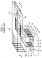
- a conventional inkjet recording head shown in Fig.1 includes a stacked chamber 17 which has thereon a pair of stacked piezoelectric elements 11 opposing to each other.
- the stacked piezoelectric elements 11 formed to be comb-like include a plurality of internal electrodes 12 at the comb-like portion. At the comb-like portion, internal electrodes 12 having one end exposed to the outside of the opposing piezoelectric elements 11, and internal electrodes 12' having one end exposed between the opposing piezoelectric elements 11 are alternately stacked.
- the three internal electrodes 12 exposing the respective one ends to the outside of the piezoelectric elements 11 are connected to one other by a longitudinal external electrode 13 for common signals, and the three internal electrodes 12' having one end exposed between the opposing piezoelectric elements 11 are connected to one other by a longitudinal external electrode for connecting common electrodes 16.
- the six internal electrodes 12 exposing to the front surface of the piezoelectric element 11 are connected to one other by a longitudinal external electrode 13 for connecting the internal electrodes 15.
- the three internal electrodes 12 exposing the respective one ends to the outside of the piezoelectric elements 11 are connected to one other by a longitudinal external electrode 14 for individual signals, and the three internal electrodes 12' having one end internally exposed are connected to one other by an external electrode 16 for connecting common electrodes
- the plurality of the external electrode 16 for connecting common electrodes in each of the piezoelectric elements 11 are connected to one other by a connecting plate 16a.
- a printing circuit board 19 mounting an IC chip 110 for switching is connected to the longitudinal external electrode 13 for the common signals and the longitudinal external electrode 14 for the individual signals through intermediary of an FPC (flexible printing circuit board) 18.
- the IC chip 110 is connected to a controlling circuit (not shown) through the intermediary of the printing circuit board 19.
- the stacked chamber 17 includes a vibration plate 171 and a nozzle plate 173 opposing to each other, and a plurality of pressure chambers 172 divided by partition plates 175 between the vibration plate 171 and the nozzle plate 173.
- Ink-ejecting nozzles 174 are formed in the nozzle plate 173 corresponding to each of the pressure chambers 172, and the pair of the piezoelectric elements 11 are fixed on the vibration plate 171 through the intermediary of an electric connection element 111.
- the FPC 18 is connected to the stacked piezoelectric elements 11 through the intermediary of the electric connection element 111.
- each of the comb-like portions of the stacked piezoelectric elements 11 vibrates by selectively applying a driving voltage from the IC chip 110 for switching through the intermediary of the printing circuit board 19 and the FPC to the piezoelectric elements 11, and the vibration is transmitted from the vibration plate 171 to the pressure chamber 172.
- ink selectively ejects from the ink-ejecting nozzles 174, and the printing is conducted on a recording medium such as recording paper.
- a signal input terminal of an interconnect is also a target of miniaturization because the ink-ejecting nozzle 174 is required to be miniaturized. Accordingly, the connection between the external electrodes 13, 14 acting as the signal input terminal of a piezoelectric signal and the FPC acting as the signal output terminal of the driving circuit are collectively conducted in view of cost and productivity.
- the plurality of the FPCs 18 are collectively connected to the external electrodes 13, 14 and the printing circuit board 19 by forming a solder plating film on the connection terminal of the FPC 18 and applying direct heating and pressure to the plating film.
- an object of the present invention is to provide an inkjet recording head which secures an excellent long-term reliability and an excellent applied voltage by averting a short-circuit between terminals and irregularity of connection resistances, and realizes a higher printing quality by suppressing the increase of a defection rate of ink ejecting characteristics even if a plenty of stacked piezoelectric elements are mounted at a higher density.
- an ink jet recording head including: a chamber housing which defines a plurality of pressure chambers; a plurality of piezoelectric elements each mounted by said chamber housing corresponding to one of said pressure chambers, each of said piezoelectric elements having thereon first and second electrodes for driving a corresponding one of said pressure chambers, each of said first and second electrodes having an electrode terminal disposed on one of end surfaces of each of said piezoelectric elements; and a circuit board having a bottom surface mounted by top surfaces of said plurality of said piezoelectric elements, a top surface mounting thereon a drive circuit and side surfaces mounting thereon a drive terminal disposed for each of said electrode terminals and connected to said drive circuit; said electrode terminal and a corresponding one of said drive terminals being connected together.
- the present invention provides, in a second aspect thereof, a method for manufacturing an inkjet recording head including the steps of: placing a solder fillet on a top end of each of a plurality of electrode terminals of a piezoelectric element; placing, on the piezoelectric element, a circuit board mounting a drive circuit thereon and a plurality of drive terminals on end surfaces thereof such that each of the top ends of the electrode terminals is in contact with the corresponding drive terminal; and heating and melting the solder fillet for connecting the drive terminal and the electrode terminal with each other.
- an inkjet recording head which secures an excellent long-term reliability and an excellent applied voltage by averting a short-circuit between terminals and irregularity of connection resistances, and realizes a higher printing quality by suppressing the increase of a defection rate of ink ejecting characteristics even if a plenty of stacked piezoelectric elements are mounted at a higher density.
- An inkjet recording head in accordance with an embodiment of the present invention shown in Fig.3 includes a stacked chamber (chamber housing) 17 and a pair of stacked piezoelectric elements 11 opposing to each other formed on the stacked chamber 17.
- the stacked piezoelectric elements 11 which provides vibration are formed to be comb-like.
- Each of the comb-like portions of both the piezoelectric elements 11 includes a plurality of internal electrodes 12. At the comb-like portion, the internal electrodes 12 having one end exposed to the outside of the opposing piezoelectric elements 11, and the internal electrodes 12 having one end exposed between the opposing piezoelectric elements 11 are alternately stacked.
- the three internal electrodes 12 exposing the respective one ends to the outside of the piezoelectric elements 11 are connected to one other by a longitudinal external electrode 13 for common signals, and the three internal electrodes 12' having one end exposed between the opposing piezoelectric elements 11 are connected to one other by a longitudinal external electrode 13 for connecting common electrodes 16.
- the six internal electrodes 12 exposing to the front surface of the piezoelectric element 11 are connected to one other by a longitudinal external electrode 13 for connecting the internal electrodes 15.
- a ceramic substrate (circuit board) 21 is disposed bridging both the stacked piezoelectric elements 11.
- the ceramic substrate 21 includes a plurality of end electrodes (drive terminals) 22 on its both side surfaces as shown in Fig.4, and each of the end electrodes 22 is connected to the corresponding external electrodes 13, 14.
- An IC chip 110 is mounted on the top central portion of the ceramic substrate 21.
- the IC chip 110 for switching includes a driving circuit selectively applying a driving voltage to the piezoelectric elements 11 through the intermediary of the respective end electrodes 22, and is connected to a controlling circuit (not shown) controlling the driving circuit through the intermediary of interconnect (not shown) connected to the ceramic substrate 21.
- the stacked chamber 17 includes a vibration plate 171 forming an ink flowing path and a nozzle plate 173 opposing to each other, and a plurality of pressure chambers 172 divided by partition plates 175 between the vibration plate 171 and the nozzle plate 173.
- Ink-ejecting nozzles 174 are formed in the nozzle plate 173 corresponding to each of the pressure chambers 172, and the pair of the piezoelectric elements 11 opposing to each other are fixed on the vibration plate 171.
- the piezoelectric elements 11 generate pressure change in the pressure chambers 172 by the vibration in the longitudinal direction in Fig.4 by an electric signal from the ceramic substrate 21, and eject ink droplets through the ink-ejecting nozzles 174 of the nozzle plate 173.
- the width of the ceramic substrate 21 is formed narrower than the distance between the outward-facing end surfaces of the piezoelectric elements 11.
- Each of the top portions of the external electrodes 13, 14 is inwardly bent and inserted between the bottom portion of the end electrode 22 and the top surface of the piezoelectric element 11.
- a solder fillet is formed on the inwardly bent portion of the external electrodes 13, 14 and connects the external electrodes 13, 14 and the end electrode 22 to each other.
- the "solder fillet" in the present invention used herein is a fillet material made of solder for connecting two members crossing substantially perpendicularly with each other for attaining similar objects and effects to those of the well-known fillet material.
- the solder fillet is preferably formed in a shape of a triangle having, as its two sides, the end electrode and the external electrode or the electrode terminal.
- concaves for end electrodes 22 were formed on both end surfaces of a ceramic substrate 21 in a pitch corresponding to a distance between a longitudinal external electrode 13 for common signals and a longitudinal external electrode 14 for individual signals as shown in Fig.5.
- the end electrode 22 may be fabricated by stacking a plurality of soft sheets each having an interconnect pattern, forming via-holes penetrating the plurality of the sheets, thermally treating the stacked sheets for curing and diving the stacked sheets along a contour line 51 passing the centers of the via holes.
- the semicircular end electrodes 22 as shown in Fig.6 can be obtained by the above simplified procedures in accordance with present Example. Since, further, the melted solder smoothly moves along the inner semicircular surface to be adhered on substantially the entire surface of the end electrodes 22, the connection between the external electrodes 13, 14 and the end electrodes 22 is secured and the procedures for the connection is simplified.
- the IC chip 110 for switching was mounted on the ceramic substrate 21, and the IC chip 110 and a controlling circuit (not shown) are connected to each other through the intermediary of the ceramic substrate 21.
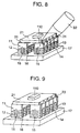
- solder paste 31 was applied on the external electrode 13 for common signals and the external electrode 14 for individual signals by printing using a metal mask located on the piezoelectric elements 11.
- the ceramic substrate 21 was precisely positioned on the solder paste-applied surface of the piezoelectric elements 11.
- a beam from a halogen lamp 32 was concentrated on and locally irradiated to the solder paste 31 between the piezoelectric elements 11 and the ceramic substrate 21. All the solder paste 31 was sequentially heated and melted by moving the local irradiation in a two-dimensional manner.
- the piezoelectric elements 11 and the ceramic substrate 21 were connected with each other by a solder fillet 23 formed by the melting and the curing of the solder paste 31 in the above procedure.
- the heating device for melting the solder paste 31 includes a xenon lamp, a laser beam irradiator and a reflow furnace which entirely heats the piezoelectric elements 11 and the ceramic substrate 21 accommodated therein.
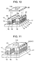
- molded solders (solid solder) 41 formed in a shape of a ball in advance were placed on the external electrodes 13, 14 corresponding to the top surface of the piezoelectric elements 11 by using a molded solder mounting apparatus (not shown), thereby retaining the molded solders on the external electrodes 13, 14 by the viscosity of the applied flux.
- the ceramic substrate 21 was precisely positioned on the piezoelectric elements 11 such that the end electrodes 22 were in contact with the row of the molded solders 41.
- the piezoelectric elements 11 and the ceramic substrate 21 were electrically and mechanically connected with each other by a solidified solder fillet 23 formed by the melting and the curing of the solder paste 31 between the piezoelectric elements 11 and the ceramic substrate 21 by using a heating device similar to that of Example 1.
- the pressurization is unnecessary and the temperature control at the time of the heating can be easily conducted. Accordingly, inconveniences such as a short-circuit conventionally occurring between the piezoelectric element 11 acting as a signal input terminal at the interconnect end and the FPC 18 acting a signal output terminal of the IC chip 110 of the external driving side, and irregularity of a connection resistance at each of the terminal connecting parts can be prevented.
- the ordinary coefficients of linear thermal expansion of the piezoelectric element 11, the conventional FPC and the ceramic substrate 21 are 1.4e -6 /°C, 18e -6 /°C and 5 to 7 e -6 /°C, respectively.
- the use of the ceramic substrate 21 enables to prevent the reduction of a dimensional accuracy due to a difference of thermal expansions between heating and cooling, and the reduction of a positional precision. Since, further, occurrence of an internal distortion at the connected portion due to the difference of the thermal expansions between the heating and the cooling can be suppressed minimum, a long-term reliability of the recording head can be secured.
Landscapes
- Engineering & Computer Science (AREA)
- Manufacturing & Machinery (AREA)
- Particle Formation And Scattering Control In Inkjet Printers (AREA)
Applications Claiming Priority (2)
| Application Number | Priority Date | Filing Date | Title |
|---|---|---|---|
| JP27172199 | 1999-09-27 | ||
| JP27172199A JP2001088302A (ja) | 1999-09-27 | 1999-09-27 | インクジェット記録ヘッド及びその製造方法 |
Publications (2)
| Publication Number | Publication Date |
|---|---|
| EP1086814A2 true EP1086814A2 (fr) | 2001-03-28 |
| EP1086814A3 EP1086814A3 (fr) | 2001-09-19 |
Family
ID=17503925
Family Applications (1)
| Application Number | Title | Priority Date | Filing Date |
|---|---|---|---|
| EP00120236A Withdrawn EP1086814A3 (fr) | 1999-09-27 | 2000-09-26 | Tête d'enregistrement jet d'encre de type multicouche et son procédé de fabrication |
Country Status (3)
| Country | Link |
|---|---|
| EP (1) | EP1086814A3 (fr) |
| JP (1) | JP2001088302A (fr) |
| CN (1) | CN1289680A (fr) |
Cited By (2)
| Publication number | Priority date | Publication date | Assignee | Title |
|---|---|---|---|---|
| EP1375150A1 (fr) * | 2002-06-19 | 2004-01-02 | Seiko Epson Corporation | Tête à jet de liquide et appareil à jet de liquide |
| EP1479112A4 (fr) * | 2002-02-25 | 2007-06-27 | Ricoh Kk | Element piezoelectrique stratifie presentant des caracteristiques de fonctionnement stables permettant d'obtenir une haute qualite d'enregistrement d'images |
Families Citing this family (4)
| Publication number | Priority date | Publication date | Assignee | Title |
|---|---|---|---|---|
| JP4640649B2 (ja) * | 2006-03-17 | 2011-03-02 | セイコーエプソン株式会社 | 液滴吐出ヘッド、画像形成装置、および成膜装置 |
| JP5168934B2 (ja) * | 2006-05-26 | 2013-03-27 | 株式会社リコー | 液体吐出ヘッド、液体吐出装置、画像形成装置、圧電アクチュエータ |
| JP4946464B2 (ja) * | 2007-01-30 | 2012-06-06 | ブラザー工業株式会社 | 液体移送装置及び液体移送装置の製造方法 |
| JP6840969B2 (ja) * | 2016-09-21 | 2021-03-10 | セイコーエプソン株式会社 | Memsデバイス、液体噴射ヘッド、及び、液体噴射装置 |
Family Cites Families (4)
| Publication number | Priority date | Publication date | Assignee | Title |
|---|---|---|---|---|
| JP3478297B2 (ja) * | 1992-06-26 | 2003-12-15 | セイコーエプソン株式会社 | インクジェット式記録ヘッド |
| US5729262A (en) * | 1993-08-31 | 1998-03-17 | Ricoh Company, Ltd. | Ink jet head including phase transition material actuators |
| JPH07285219A (ja) * | 1994-04-19 | 1995-10-31 | Ricoh Co Ltd | インクジェットヘッド |
| JPH11254670A (ja) * | 1998-03-10 | 1999-09-21 | Nec Corp | インクジェットヘッド |
-
1999
- 1999-09-27 JP JP27172199A patent/JP2001088302A/ja active Pending
-
2000
- 2000-09-26 EP EP00120236A patent/EP1086814A3/fr not_active Withdrawn
- 2000-09-27 CN CN 00124674 patent/CN1289680A/zh active Pending
Cited By (3)
| Publication number | Priority date | Publication date | Assignee | Title |
|---|---|---|---|---|
| EP1479112A4 (fr) * | 2002-02-25 | 2007-06-27 | Ricoh Kk | Element piezoelectrique stratifie presentant des caracteristiques de fonctionnement stables permettant d'obtenir une haute qualite d'enregistrement d'images |
| EP1375150A1 (fr) * | 2002-06-19 | 2004-01-02 | Seiko Epson Corporation | Tête à jet de liquide et appareil à jet de liquide |
| US6886923B2 (en) | 2002-06-19 | 2005-05-03 | Seiko Epson Corporation | Small-sized liquid-jet head and liquid-jet apparatus with increased number of arrays of nozzle orifices |
Also Published As
| Publication number | Publication date |
|---|---|
| CN1289680A (zh) | 2001-04-04 |
| EP1086814A3 (fr) | 2001-09-19 |
| JP2001088302A (ja) | 2001-04-03 |
Similar Documents
| Publication | Publication Date | Title |
|---|---|---|
| US7766458B2 (en) | Inkjet head capable of suppressing hindrance of deformation of a piezoelectric element | |
| US6113216A (en) | Wide array thermal ink-jet print head | |
| US5434607A (en) | Attachment of nozzle plate to flexible circuit for facilitating assembly of printhead | |
| JP5211631B2 (ja) | 液滴吐出装置及びその製造方法 | |
| EP1086814A2 (fr) | Tête d'enregistrement jet d'encre de type multicouche et son procédé de fabrication | |
| KR20020035829A (ko) | 고온의 액상 매체 분사용 인쇄 헤드 및 금속 납땜으로이루어진 접합부의 제조 방법 | |
| JP3555638B2 (ja) | インクジェット式記録ヘッド | |
| JP2006278964A (ja) | 基板接合構造の製造方法及び端子形成基板 | |
| JP4109898B2 (ja) | インクジェット記録ヘッド | |
| JPH07156376A (ja) | インクジェットヘッド及びその製造方法及びその製造方法に使用する導体パタン | |
| US8551275B2 (en) | Adhesive application method and terminal joining method | |
| JPH09286103A (ja) | インクジェット式記録ヘッド | |
| JP4192830B2 (ja) | 配線部材の接続方法 | |
| JPH09226118A (ja) | インクジェットヘッド | |
| JP3622484B2 (ja) | 圧電アクチュエータ及びこれを用いたインクジェットヘッド | |
| JPH10250053A (ja) | インク噴射装置およびその製造方法 | |
| JP2005131948A (ja) | ヘッドモジュール、液体吐出ヘッド、液体吐出装置、ヘッドモジュールの製造方法及び液体吐出ヘッドの製造方法 | |
| JP2001096783A (ja) | サーマルヘッド | |
| JP7056354B2 (ja) | 記録装置、配線部材及び配線部材の製造方法 | |
| JP2579732Y2 (ja) | 円筒型熱印字素子 | |
| JP2025162673A (ja) | 液体吐出ヘッドの製造方法および液体吐出ヘッド | |
| JP2002178515A (ja) | インクジェット記録ヘッド用フレキシブルケーブル、及びその製造方法 | |
| JPH05229160A (ja) | サーマルヘッド | |
| JP2004262190A (ja) | 電気接続構造、これを用いたインクジェット記録ヘッド及び記録装置 | |
| JP2005138521A (ja) | 液体吐出ヘッド及び液体吐出装置 |
Legal Events
| Date | Code | Title | Description |
|---|---|---|---|
| PUAI | Public reference made under article 153(3) epc to a published international application that has entered the european phase |
Free format text: ORIGINAL CODE: 0009012 |
|
| AK | Designated contracting states |
Kind code of ref document: A2 Designated state(s): DE FR IT Kind code of ref document: A2 Designated state(s): AT BE CH CY DE DK ES FI FR GB GR IE IT LI LU MC NL PT SE |
|
| AX | Request for extension of the european patent |
Free format text: AL;LT;LV;MK;RO;SI |
|
| PUAL | Search report despatched |
Free format text: ORIGINAL CODE: 0009013 |
|
| AK | Designated contracting states |
Kind code of ref document: A3 Designated state(s): AT BE CH CY DE DK ES FI FR GB GR IE IT LI LU MC NL PT SE |
|
| AX | Request for extension of the european patent |
Free format text: AL;LT;LV;MK;RO;SI |
|
| 17P | Request for examination filed |
Effective date: 20010809 |
|
| AKX | Designation fees paid |
Free format text: DE FR IT |
|
| RAP1 | Party data changed (applicant data changed or rights of an application transferred) |
Owner name: FUJI XEROX CO., LTD. |
|
| STAA | Information on the status of an ep patent application or granted ep patent |
Free format text: STATUS: THE APPLICATION HAS BEEN WITHDRAWN |
|
| 18W | Application withdrawn |
Withdrawal date: 20021010 |