EP1087431A2 - Procédé et dispositif pour former une couche de germination dopée deposée par pulvérisation - Google Patents
Procédé et dispositif pour former une couche de germination dopée deposée par pulvérisation Download PDFInfo
- Publication number
- EP1087431A2 EP1087431A2 EP00308436A EP00308436A EP1087431A2 EP 1087431 A2 EP1087431 A2 EP 1087431A2 EP 00308436 A EP00308436 A EP 00308436A EP 00308436 A EP00308436 A EP 00308436A EP 1087431 A2 EP1087431 A2 EP 1087431A2
- Authority
- EP
- European Patent Office
- Prior art keywords
- copper
- substrate
- target
- doped
- phosphorus
- Prior art date
- Legal status (The legal status is an assumption and is not a legal conclusion. Google has not performed a legal analysis and makes no representation as to the accuracy of the status listed.)
- Withdrawn
Links
Images
Classifications
-
- H—ELECTRICITY
- H10—SEMICONDUCTOR DEVICES; ELECTRIC SOLID-STATE DEVICES NOT OTHERWISE PROVIDED FOR
- H10W—GENERIC PACKAGES, INTERCONNECTIONS, CONNECTORS OR OTHER CONSTRUCTIONAL DETAILS OF DEVICES COVERED BY CLASS H10
- H10W20/00—Interconnections in chips, wafers or substrates
- H10W20/01—Manufacture or treatment
- H10W20/031—Manufacture or treatment of conductive parts of the interconnections
- H10W20/032—Manufacture or treatment of conductive parts of the interconnections of conductive barrier, adhesion or liner layers
- H10W20/042—Manufacture or treatment of conductive parts of the interconnections of conductive barrier, adhesion or liner layers the barrier, adhesion or liner layers being seed or nucleation layers
- H10W20/043—Manufacture or treatment of conductive parts of the interconnections of conductive barrier, adhesion or liner layers the barrier, adhesion or liner layers being seed or nucleation layers for electroplating
-
- C—CHEMISTRY; METALLURGY
- C23—COATING METALLIC MATERIAL; COATING MATERIAL WITH METALLIC MATERIAL; CHEMICAL SURFACE TREATMENT; DIFFUSION TREATMENT OF METALLIC MATERIAL; COATING BY VACUUM EVAPORATION, BY SPUTTERING, BY ION IMPLANTATION OR BY CHEMICAL VAPOUR DEPOSITION, IN GENERAL; INHIBITING CORROSION OF METALLIC MATERIAL OR INCRUSTATION IN GENERAL
- C23C—COATING METALLIC MATERIAL; COATING MATERIAL WITH METALLIC MATERIAL; SURFACE TREATMENT OF METALLIC MATERIAL BY DIFFUSION INTO THE SURFACE, BY CHEMICAL CONVERSION OR SUBSTITUTION; COATING BY VACUUM EVAPORATION, BY SPUTTERING, BY ION IMPLANTATION OR BY CHEMICAL VAPOUR DEPOSITION, IN GENERAL
- C23C14/00—Coating by vacuum evaporation, by sputtering or by ion implantation of the coating forming material
- C23C14/06—Coating by vacuum evaporation, by sputtering or by ion implantation of the coating forming material characterised by the coating material
- C23C14/14—Metallic material, boron or silicon
- C23C14/18—Metallic material, boron or silicon on other inorganic substrates
-
- H—ELECTRICITY
- H10—SEMICONDUCTOR DEVICES; ELECTRIC SOLID-STATE DEVICES NOT OTHERWISE PROVIDED FOR
- H10P—GENERIC PROCESSES OR APPARATUS FOR THE MANUFACTURE OR TREATMENT OF DEVICES COVERED BY CLASS H10
- H10P14/00—Formation of materials, e.g. in the shape of layers or pillars
- H10P14/40—Formation of materials, e.g. in the shape of layers or pillars of conductive or resistive materials
- H10P14/42—Formation of materials, e.g. in the shape of layers or pillars of conductive or resistive materials using a gas or vapour
- H10P14/44—Physical vapour deposition [PVD]
-
- H—ELECTRICITY
- H10—SEMICONDUCTOR DEVICES; ELECTRIC SOLID-STATE DEVICES NOT OTHERWISE PROVIDED FOR
- H10W—GENERIC PACKAGES, INTERCONNECTIONS, CONNECTORS OR OTHER CONSTRUCTIONAL DETAILS OF DEVICES COVERED BY CLASS H10
- H10W20/00—Interconnections in chips, wafers or substrates
- H10W20/01—Manufacture or treatment
- H10W20/031—Manufacture or treatment of conductive parts of the interconnections
- H10W20/032—Manufacture or treatment of conductive parts of the interconnections of conductive barrier, adhesion or liner layers
- H10W20/033—Manufacture or treatment of conductive parts of the interconnections of conductive barrier, adhesion or liner layers in openings in dielectrics
-
- H—ELECTRICITY
- H10—SEMICONDUCTOR DEVICES; ELECTRIC SOLID-STATE DEVICES NOT OTHERWISE PROVIDED FOR
- H10W—GENERIC PACKAGES, INTERCONNECTIONS, CONNECTORS OR OTHER CONSTRUCTIONAL DETAILS OF DEVICES COVERED BY CLASS H10
- H10W20/00—Interconnections in chips, wafers or substrates
- H10W20/40—Interconnections external to wafers or substrates, e.g. back-end-of-line [BEOL] metallisations or vias connecting to gate electrodes
- H10W20/41—Interconnections external to wafers or substrates, e.g. back-end-of-line [BEOL] metallisations or vias connecting to gate electrodes characterised by their conductive parts
- H10W20/425—Barrier, adhesion or liner layers
-
- H—ELECTRICITY
- H10—SEMICONDUCTOR DEVICES; ELECTRIC SOLID-STATE DEVICES NOT OTHERWISE PROVIDED FOR
- H10W—GENERIC PACKAGES, INTERCONNECTIONS, CONNECTORS OR OTHER CONSTRUCTIONAL DETAILS OF DEVICES COVERED BY CLASS H10
- H10W20/00—Interconnections in chips, wafers or substrates
- H10W20/40—Interconnections external to wafers or substrates, e.g. back-end-of-line [BEOL] metallisations or vias connecting to gate electrodes
- H10W20/41—Interconnections external to wafers or substrates, e.g. back-end-of-line [BEOL] metallisations or vias connecting to gate electrodes characterised by their conductive parts
- H10W20/44—Conductive materials thereof
- H10W20/4403—Conductive materials thereof based on metals, e.g. alloys, metal silicides
- H10W20/4421—Conductive materials thereof based on metals, e.g. alloys, metal silicides the principal metal being copper
- H10W20/4424—Copper alloys
Definitions
- the present invention relates to the deposition of a layer on a substrate. More specifically, the invention relates to deposition of a doped layer on a substrate.
- multilevel interconnect technology which provides the conductive paths between the devices of an integrated circuit (IC) and other electronic devices.
- IC integrated circuit
- VLSI very large scale integration
- ULSI ultra large scale integration
- Aluminum has traditionally been the choice of conductive materials used in metallization. However, smaller feature sizes have created a need for a conductive material with lower resistivity than aluminum. Copper is now being considered as an interconnect material to replace or complement aluminum because copper has a lower resistivity (1.7 ⁇ -cm compared to 3.1 ⁇ -cm for aluminum) and higher current carrying capacity.
- CVD chemical vapor deposition
- PVD physical vapor deposition
- electroplating processes are being developed for deposition of conductive material, particularly copper, to fill small features on a substrate.
- electroplating has its own challenges in depositing uniformly on a substrate.
- Electroplating uses an electrically conductive seed layer, such as a copper layer conformally deposited by CVD or PVD, to initiate the electroplating deposition process on the substrate.
- CVD chemical vapor deposition
- PVD is the current choice for depositing the seed layer conformally over the feature.
- PVD of copper tends to agglomerate across the deposition surface and in the lines and vias due to surface diffusion of the copper material.
- a high surface diffusivity of copper which is a function of the deposition temperature, causes the deposited copper film to agglomerate such that the film will either dewet, thereby becoming discontinuous, and/or roughen such that the agglomeration reduces the overall surface energy of the exposed copper surface.
- This agglomeration has the adverse effect on a subsequent electroplating process such that either the discontinuous film will lead to micro-voids in the electroplated copper or the roughened surface will provide a localized electrical field, also resulting in micro-voids and other nonuniformities.
- the electroplated layer such as a seed layer, is nonuniformly deposited on the substrate, then the current will not be evenly distributed over the surface of the seed layer and may result in nonuniform deposition of a subsequent electroplated layer on the substrate.
- copper is highly susceptible to oxidation, which increases the resistivity of a copper feature. Oxidation can occur when the substrate is moved between chambers and exposed to ambient conditions or in a particular process that exposes the copper to an oxygen source. Oxidation of copper increases the resistivity of the lines and vias formed.
- the present invention generally provides a method and apparatus for forming a doped layer on a substrate to improve uniformity of subsequent deposition thereover.
- the layer is deposited by a sputtering process, such as physical vapor deposition (PVD) or Ionized Metal Plasma (IMP) PVD, using a doped target of conductive material.
- the conductive material such as copper
- a dopant such as phosphorus, boron, indium, tin, beryllium, or combinations thereof, to improve deposition uniformity of the doped layer over the substrate surface and to reduce oxidation of the conductive material.
- a dopant such as phosphorus
- stabilizes the conductive material surface such as a copper surface, and lessens the surface diffusivity of the conductive material.
- the overall surface diffusivity of copper is reduced such that the tendency to agglomerate or to become discontinuous is reduced, thereby allowing the deposition of a smoother conductive film and thereby reducing localized agglomeration of the conductive material.
- the smoother film is highly desirable for subsequent deposition processes.
- a conductive material, such as copper can be deposited on the deposited doped layer by a variety of processes including PVD, chemical vapor deposition (CVD), electroplating, electroless deposition and other deposition processes.
- the present invention provides an apparatus for depositing a material on a substrate, comprising a processing chamber and a doped conductive target.
- the target comprises a conductive material selected from the group of copper, tungsten, aluminum or combinations thereof and a doping material selected from the group of phosphorus, boron, indium, tin, beryllium or combinations thereof.
- the invention provides a doped conductive target for sputtering a layer on a substrate.
- the doped conductive target comprises a conductive material selected from the group of copper, tungsten, aluminum or combinations thereof and a doping material selected from the group of phosphorus, boron, indium, tin, beryllium or combinations thereof.
- the invention provides a substrate having a doped seed layer deposited by a sputtering process on the substrate.
- the doped seed layer comprises a conductive material selected from the group of copper, tungsten, aluminum or combinations thereof and a doping material selected from the group of phosphorus, boron, indium, tin, beryllium or combinations thereof.
- the invention provides a method of sputtering a layer on a substrate, comprising generating a plasma in a substrate processing chamber, sputtering material from a doped conductive target, the target comprising a conductive material selected from the group of copper, tungsten, aluminum or combinations thereof and a doping material selected from the group of phosphorus, boron, indium, tin, beryllium or combinations thereof, and depositing the sputtered doped material on the substrate.
- a conductive layer of copper can be deposited over the sputtered doped material, preferably, by an electroplating process.
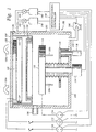
- Figure 1 is a schematic cross-sectional view of an IMP chamber.
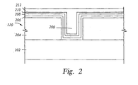
- Figure 2 is a schematic cross-sectional view of a substrate with a seed layer formed on the substrate.
- the present invention provides a method and apparatus for forming a doped layer on a substrate, preferably using a sputtering process.
- the doped layer preferably comprises copper doped with phosphorus.
- Figure 1 is a schematic cross-sectional view of an IMP chamber 100, capable of generating a relatively high density plasma, i.e., one with a capability to ionize a significant fraction of both the process gas (typically argon) and the sputtered target material.
- a sputtering chamber known as an IMP VectraTM chamber, is available from Applied Materials, Inc. of Santa Clara, California.
- the IMP chamber can be integrated into an EnduraTM platform, also available from Applied Materials, Inc.
- the IMP process provides a higher density plasma than standard PVD that causes the sputtered target material to become ionized as the sputtered material passes therethrough.
- the ionization enables the sputtered material to be attracted in a substantially perpendicular direction to a biased substrate surface and to deposit a thin layer even in high aspect ratio features.
- the high density plasma is supported by a coil 122 internal to the chamber through which AC current is passed. The current couples with the atoms of gas and sputtered material to ionize a significant portion thereof.
- the chamber 100 includes sidewalls 101, lid 102, and bottom 103.
- the lid 102 includes a target backing plate 104 which supports a target 105 of the material to be deposited.
- the target 105 is preferably made of a conductive material and a doping material.
- the conductive material is selected from a group of copper, tungsten, aluminum or combinations thereof.
- the doping material is selected from a group of phosphorus, boron, indium, tin, beryllium or combinations thereof.
- the conductive material is copper and the doping material is phosphorus.
- the percentage by weight of the doping material is from about 0.01% to about 15%, preferably about 0.01% to about 0.5%.
- the target can be prepared, for example, by uniformly mixing a phosphorus oxide into a molten copper material where the oxygen is thermally or chemically released and the remaining phosphorus and copper formed into a target. A number of processes known to metallurgists are possible to produce a doped target.
- An opening 108 in the chamber 100 provides access for a robot (not shown) to deliver and retrieve substrates 110 to and from the chamber 100.
- a substrate support 112 supports the substrate 110 in the chamber and is typically grounded.
- the substrate support 112 is mounted on a lift motor 114 that raises and lowers the substrate support 112 and a substrate 110 disposed thereon.
- a lift plate 116 connected to a lift motor 118 is mounted in the chamber 100 and raises and lowers pins 120a, 120b mounted in the substrate support 112. The pins 120a, 120b raise and lower the substrate 110 from and to the surface of the substrate support 112.
- a coil 122 is mounted between the substrate support 112 and the target 105 and provides inductively-coupled magnetic fields in the chamber 100 to assist in generating and maintaining a plasma between the target 105 and substrate 110.
- the coil 122 is sputtered due to its location between the target and the substrate 110 and preferably is made of similar constituents as the target 105.
- the coil 122 could be made of copper and phosphorus.
- the doping percentage of the coil 122 could vary compared to the target doping percentage depending on the desired layer composition and is empirically determined by varying the relative doping percentages. Power supplied to the coil 122 densifies the plasma which ionizes the sputtered material. The ionized material is then directed toward the substrate 110 and deposited thereon.
- a shield 124 is disposed in the chamber 100 to shield the chamber sidewalls 101 from the sputtered material.
- the shield 124 also supports the coil 122 by coil supports 126.
- the coil supports 126 electrically insulate the coil 122 from the shield 124 and the chamber 100 and can be made of similar material as the coil.
- the clamp ring 128 is mounted between the coil 122 and the substrate support 112 and shields an outer edge and backside of the substrate from sputtered materials when the substrate 110 is raised into a processing position to engage the lower portion of the clamp ring 128.
- the shield 124 supports the clamp ring 128 when the substrate 110 is lowered below the shield 124 to enable substrate transfer.
- a power supply 130 delivers preferably DC power to the target 105 to cause the processing gas to form a plasma, although RF power can be used.
- Magnets 106a, 106b disposed behind the target backing plate 104 increase the density of electrons adjacent to the target 105, thus increasing ionization at the target to increase the sputtering efficiency.
- the magnets 106a, 106b generate magnetic field lines generally parallel to the face of the target, around which electrons are trapped in spinning orbits to increase the likelihood of a collision with, and ionization of, a gas atom for sputtering.
- a power supply 132 preferably a RF power supply, supplies electrical power to the coil 122 to couple with and increase the density of the plasma.
- Another power supply 134 typically a DC power supply, biases the substrate support 112 with respect to the plasma and provides directional attraction (or repulsion) of the ionized sputtered material toward the substrate 110.
- Processing gas such as an inert gas of argon or helium or a reactive gas such as nitrogen, is supplied to the chamber 100 through a gas inlet 136 from gas sources 138, 140 as metered by respective mass flow controllers 142, 144.
- a vacuum pump 146 is connected to the chamber 100 at an exhaust port 148 to exhaust the chamber 100 and maintain the desired pressure in the chamber 100.
- a controller 149 generally controls the functions of the power supplies, lift motors, mass flow controllers for gas injection, vacuum pump, and other associated chamber components and functions.
- the controller 149 controls the power supply 130 coupled to the target 105 to cause the processing gas to form a plasma and sputter the target material.
- the controller 149 also controls the power supply 132 coupled to the coil 122 to increase the density of the plasma and ionize the sputtered material.
- the controller 149 also controls the power supply 134 to provide directional attraction of the ionized sputtered material to the substrate surface.
- the controller 149 executes system control software stored in a memory, which in the preferred embodiment is a hard disk drive, and can include analog and digital input/output boards, interface boards, and stepper motor controller boards (not shown). Optical and/or magnetic sensors (not shown) are generally used to move and determine the position of movable mechanical assemblies.
- a noble gas such as helium or argon
- the power supply 130 delivers about 200 watts (W) to about 6 kW, preferably about 750 W to about 1.5 kW to the target 105.
- the power supply 132 delivers about 500 W to about 5 kW, preferably about 1.5 kW to about 2.5 kW AC to the coil 122.
- the power supply 134 delivers about 0 W to about 600 W, preferably about 350 W to about 500 W to the substrate support 112 with a duty cycle between 0% to 100% and preferably about 50% to about 75%.
- a surface temperature between about -50°C to about 150°C, preferably below 50°C is useful for processing during the seed layer deposition.
- the copper/phosphorus material is deposited on the substrate to a thickness of about 500 ⁇ to about 4000 ⁇ , preferably about 2000 ⁇ .
- FIG. 2 is a schematic cross-sectional view of an exemplary substrate 110 formed according to a process of the invention.
- a dielectric layer 204 is deposited on the substrate 110 and etched to form the feature 200, such as a via, contact, trench or line.
- the term "substrate” is broadly defined as the underlying material and can include a series of underlying layers.
- the dielectric layer 204 can be a pre-metal dielectric layer deposited over a silicon wafer or an interlevel dielectric layer.
- a liner layer 206 such as a Ta layer, is deposited on the dielectric layer 204 as a transition layer to promote adhesion to the underlying material and reduce contact/via resistance.
- the liner layer 206 is preferably deposited using a IMP PVD process and can be deposited by other PVD processes, such as collimated or long throw sputtering or other methods such as CVD.
- Collimated sputtering is generally performed by placing a collimator (not shown) between the target and the substrate to filter sputtered material traveling obliquely through the collimator.
- Long throw sputtering is generally performed by increasing the spacing between the target and the substrate. The increased distance increases the probability that the sputtered material reaching the substrate is directed normal to the substrate surface.
- a barrier layer 208 of tantalum nitride (TaN) is deposited on the liner layer 206 using PVD, and preferably an IMP PVD process, especially for high aspect ratio features.
- the barrier layer prevents diffusion of copper into adjacent layers. While Ta/TaN are preferred, other liner and/or barrier layers that can be used are titanium (Ti), titanium nitride (TiN), tungsten (W), tungsten nitride (WN) and other refractory metals and their nitrided counterparts.
- a doped seed layer 210 is deposited over the TaN barrier layer 208, using PVD and preferably IMP PVD.
- the seed layer 210 is deposited by sputtering a conductive target preferably doped with phosphorus.
- the conductive material is selected from the group of copper, tungsten, aluminum or combinations thereof.
- the doping material is selected from the group of phosphorus, boron, indium, tin, beryllium or combinations thereof.
- the conductive material is copper and the doping material is phosphorus.
- the percentage by weight of the doping material is from about 0.01% to about 15%, preferably about 0.01% to about 0.5%.
- the copper/phosphorus material is deposited over the barrier layer 208 as a seed layer for a subsequent copper layer 212.
- the copper layer 212 can be deposited by PVD, IMP, CVD, electroplating, electroless deposition, evaporation, or other known methods. Preferably, copper layer 212 is deposited using electroplating techniques.
- An exemplary electroplating system is described in co-pending U.S. Pat. Appl. No. 09/350,877, filed on July 9, 1999, and in co-pending U.S. Pat. Appl. 09/289,074, filed on April 8, 1999, and are incorporated herein by reference.
- a description of an electroplating chemistry, particularly the composition of the electrolyte and additives, is provided in co-pending U.S. Pat. Appl. No. 09/245,780, filed on February 5, 1999 and is incorporated herein by reference.
- Subsequent processing can include planarization by chemical mechanical polishing (CMP), additional deposition of layers, etching, and other processes known to substrate manufacturing.
- CMP chemical mechanical polishing
- the doping material is believed to reduce surface diffusivity of the sputtered conductive material, such as copper, as the sputtered material is deposited. Less agglomeration occurs with the doping and the sputtered conductive layer is deposited more conformally with less voids. For a subsequent process, such as electroplating, that is affected by the integrity of an underlying seed layer, the doped layer yields a more uniform subsequent layer deposited thereon.
- Phosphorus and other doping materials also reduce copper oxidation due to their generally greater affinity for oxygen than copper at processing temperatures. It is believed that oxygen reaching the substrate surface prefers initiating bonds with the dopant, leaving the copper less likely to be oxidized. A lower level of oxidation reduces the resistance of both the target material and the deposited layer of the target material. Reduced oxidation also assists in reducing corrosion in post-deposition processing such as wet CMP processing.
- the phosphorus is also believed to harden the target and the deposited layer. Empirical evidence suggests that harder targets result in reduced arcing between the target and an adjacent structure, where the arcing dislodges unwanted pieces of the target (splats) that are deposited on the substrate and contaminates the deposition. The phosphorus is also believed to lower the melting temperature of the copper, so that surface mobility and planarization can occur at lower temperatures.
Landscapes
- Chemical & Material Sciences (AREA)
- Inorganic Chemistry (AREA)
- Chemical Kinetics & Catalysis (AREA)
- Engineering & Computer Science (AREA)
- Materials Engineering (AREA)
- Mechanical Engineering (AREA)
- Metallurgy (AREA)
- Organic Chemistry (AREA)
- Electrodes Of Semiconductors (AREA)
- Internal Circuitry In Semiconductor Integrated Circuit Devices (AREA)
- Physical Vapour Deposition (AREA)
- Physical Deposition Of Substances That Are Components Of Semiconductor Devices (AREA)
Applications Claiming Priority (2)
| Application Number | Priority Date | Filing Date | Title |
|---|---|---|---|
| US09/406,325 US6432819B1 (en) | 1999-09-27 | 1999-09-27 | Method and apparatus of forming a sputtered doped seed layer |
| US406325 | 1999-09-27 |
Publications (2)
| Publication Number | Publication Date |
|---|---|
| EP1087431A2 true EP1087431A2 (fr) | 2001-03-28 |
| EP1087431A3 EP1087431A3 (fr) | 2003-05-21 |
Family
ID=23607481
Family Applications (1)
| Application Number | Title | Priority Date | Filing Date |
|---|---|---|---|
| EP00308436A Withdrawn EP1087431A3 (fr) | 1999-09-27 | 2000-09-26 | Procédé et dispositif pour former une couche de germination dopée deposée par pulvérisation |
Country Status (5)
| Country | Link |
|---|---|
| US (2) | US6432819B1 (fr) |
| EP (1) | EP1087431A3 (fr) |
| JP (1) | JP2001220667A (fr) |
| KR (1) | KR20010030504A (fr) |
| SG (1) | SG86443A1 (fr) |
Cited By (1)
| Publication number | Priority date | Publication date | Assignee | Title |
|---|---|---|---|---|
| WO2003088203A1 (fr) | 2002-04-11 | 2003-10-23 | Genoa Color Technologies Ltd. | Dispositifs et procedes d'affichage couleur presentant de meilleurs attributs |
Families Citing this family (208)
| Publication number | Priority date | Publication date | Assignee | Title |
|---|---|---|---|---|
| US6569751B1 (en) * | 2000-07-17 | 2003-05-27 | Lsi Logic Corporation | Low via resistance system |
| US6355561B1 (en) * | 2000-11-21 | 2002-03-12 | Micron Technology, Inc. | ALD method to improve surface coverage |
| US6979646B2 (en) * | 2000-12-29 | 2005-12-27 | Intel Corporation | Hardening of copper to improve copper CMP performance |
| JP2002217292A (ja) * | 2001-01-23 | 2002-08-02 | Hitachi Ltd | 半導体集積回路装置および半導体集積回路装置の製造方法 |
| US6951804B2 (en) | 2001-02-02 | 2005-10-04 | Applied Materials, Inc. | Formation of a tantalum-nitride layer |
| US6740221B2 (en) | 2001-03-15 | 2004-05-25 | Applied Materials Inc. | Method of forming copper interconnects |
| KR100499557B1 (ko) * | 2001-06-11 | 2005-07-07 | 주식회사 하이닉스반도체 | 반도체소자의 배선 형성방법 |
| JP4711624B2 (ja) * | 2001-10-26 | 2011-06-29 | アプライド マテリアルズ インコーポレイテッド | 銅電極形成アプリケーションのためのald窒化タンタル及びアルファ相タンタルの集積 |
| US7521366B2 (en) * | 2001-12-12 | 2009-04-21 | Lg Display Co., Ltd. | Manufacturing method of electro line for liquid crystal display device |
| WO2003063067A1 (fr) * | 2002-01-24 | 2003-07-31 | Chatterbox Systems, Inc. | Procedes et systemes de localisation de position dans des textes imprimes et de diffusion d'informations multimedia |
| US7138014B2 (en) | 2002-01-28 | 2006-11-21 | Applied Materials, Inc. | Electroless deposition apparatus |
| US6824666B2 (en) * | 2002-01-28 | 2004-11-30 | Applied Materials, Inc. | Electroless deposition method over sub-micron apertures |
| US20030188974A1 (en) * | 2002-04-03 | 2003-10-09 | Applied Materials, Inc. | Homogeneous copper-tin alloy plating for enhancement of electro-migration resistance in interconnects |
| US6905622B2 (en) * | 2002-04-03 | 2005-06-14 | Applied Materials, Inc. | Electroless deposition method |
| US6899816B2 (en) * | 2002-04-03 | 2005-05-31 | Applied Materials, Inc. | Electroless deposition method |
| JP3797317B2 (ja) * | 2002-05-30 | 2006-07-19 | 住友金属鉱山株式会社 | 透明導電性薄膜用ターゲット、透明導電性薄膜およびその製造方法、ディスプレイ用電極材料、有機エレクトロルミネッセンス素子 |
| US20040118699A1 (en) * | 2002-10-02 | 2004-06-24 | Applied Materials, Inc. | Homogeneous copper-palladium alloy plating for enhancement of electro-migration resistance in interconnects |
| US6821909B2 (en) * | 2002-10-30 | 2004-11-23 | Applied Materials, Inc. | Post rinse to improve selective deposition of electroless cobalt on copper for ULSI application |
| US7654221B2 (en) * | 2003-10-06 | 2010-02-02 | Applied Materials, Inc. | Apparatus for electroless deposition of metals onto semiconductor substrates |
| US7827930B2 (en) * | 2004-01-26 | 2010-11-09 | Applied Materials, Inc. | Apparatus for electroless deposition of metals onto semiconductor substrates |
| US20070111519A1 (en) * | 2003-10-15 | 2007-05-17 | Applied Materials, Inc. | Integrated electroless deposition system |
| US7064065B2 (en) * | 2003-10-15 | 2006-06-20 | Applied Materials, Inc. | Silver under-layers for electroless cobalt alloys |
| US7465358B2 (en) * | 2003-10-15 | 2008-12-16 | Applied Materials, Inc. | Measurement techniques for controlling aspects of a electroless deposition process |
| WO2005038084A2 (fr) * | 2003-10-17 | 2005-04-28 | Applied Materials, Inc. | Depot autocatalytique selectif a auto-amorçage d'une couche protectrice de cuivre a base d'alliages contenant du cobalt |
| US7205233B2 (en) | 2003-11-07 | 2007-04-17 | Applied Materials, Inc. | Method for forming CoWRe alloys by electroless deposition |
| US20050098427A1 (en) * | 2003-11-11 | 2005-05-12 | Taiwan Semiconductor Manufacturing Co., Ltd. | RF coil design for improved film uniformity of an ion metal plasma source |
| US20060003570A1 (en) * | 2003-12-02 | 2006-01-05 | Arulkumar Shanmugasundram | Method and apparatus for electroless capping with vapor drying |
| US20050230350A1 (en) * | 2004-02-26 | 2005-10-20 | Applied Materials, Inc. | In-situ dry clean chamber for front end of line fabrication |
| US20050266173A1 (en) * | 2004-05-26 | 2005-12-01 | Tokyo Electron Limited | Method and apparatus of distributed plasma processing system for conformal ion stimulated nanoscale deposition process |
| US20060251801A1 (en) | 2005-03-18 | 2006-11-09 | Weidman Timothy W | In-situ silicidation metallization process |
| US7651934B2 (en) | 2005-03-18 | 2010-01-26 | Applied Materials, Inc. | Process for electroless copper deposition |
| WO2006102318A2 (fr) | 2005-03-18 | 2006-09-28 | Applied Materials, Inc. | Procede de depot autocatalytique sur un contact contenant du silicium ou du siliciure |
| US7285496B2 (en) * | 2005-04-28 | 2007-10-23 | Intel Corporation | Hardening of copper to improve copper CMP performance |
| JP4923450B2 (ja) * | 2005-07-01 | 2012-04-25 | 富士ゼロックス株式会社 | バッチ処理支援装置および方法、プログラム |
| US20070012559A1 (en) * | 2005-07-13 | 2007-01-18 | Applied Materials, Inc. | Method of improving magnetron sputtering of large-area substrates using a removable anode |
| US20070084720A1 (en) * | 2005-07-13 | 2007-04-19 | Akihiro Hosokawa | Magnetron sputtering system for large-area substrates having removable anodes |
| US20070012558A1 (en) * | 2005-07-13 | 2007-01-18 | Applied Materials, Inc. | Magnetron sputtering system for large-area substrates |
| US20070012663A1 (en) * | 2005-07-13 | 2007-01-18 | Akihiro Hosokawa | Magnetron sputtering system for large-area substrates having removable anodes |
| US20070051616A1 (en) * | 2005-09-07 | 2007-03-08 | Le Hienminh H | Multizone magnetron assembly |
| US20070056843A1 (en) * | 2005-09-13 | 2007-03-15 | Applied Materials, Inc. | Method of processing a substrate using a large-area magnetron sputtering chamber with individually controlled sputtering zones |
| US20070056850A1 (en) * | 2005-09-13 | 2007-03-15 | Applied Materials, Inc. | Large-area magnetron sputtering chamber with individually controlled sputtering zones |
| US7588668B2 (en) | 2005-09-13 | 2009-09-15 | Applied Materials, Inc. | Thermally conductive dielectric bonding of sputtering targets using diamond powder filler or thermally conductive ceramic fillers |
| US20070071888A1 (en) * | 2005-09-21 | 2007-03-29 | Arulkumar Shanmugasundram | Method and apparatus for forming device features in an integrated electroless deposition system |
| US20070158179A1 (en) * | 2006-01-11 | 2007-07-12 | Anthony Ciancio | Method and apparatus for improving symmetry of a layer deposited on a semiconductor substrate |
| US7749361B2 (en) * | 2006-06-02 | 2010-07-06 | Applied Materials, Inc. | Multi-component doping of copper seed layer |
| US8791018B2 (en) * | 2006-12-19 | 2014-07-29 | Spansion Llc | Method of depositing copper using physical vapor deposition |
| US7867900B2 (en) | 2007-09-28 | 2011-01-11 | Applied Materials, Inc. | Aluminum contact integration on cobalt silicide junction |
| JP5420328B2 (ja) | 2008-08-01 | 2014-02-19 | 三菱マテリアル株式会社 | フラットパネルディスプレイ用配線膜形成用スパッタリングターゲット |
| JP5541651B2 (ja) * | 2008-10-24 | 2014-07-09 | 三菱マテリアル株式会社 | 薄膜トランジスター用配線膜形成用スパッタリングターゲット |
| JP5651298B2 (ja) * | 2008-10-24 | 2015-01-07 | シチズン時計マニュファクチャリング株式会社 | プラズマ援用反応性薄膜形成装置およびそれを用いた薄膜形成方法 |
| JP5457754B2 (ja) * | 2009-08-07 | 2014-04-02 | 株式会社日立ハイテクノロジーズ | 透過型電極体を用いたプラズマ処理装置 |
| US9324576B2 (en) | 2010-05-27 | 2016-04-26 | Applied Materials, Inc. | Selective etch for silicon films |
| US8508018B2 (en) * | 2010-09-24 | 2013-08-13 | Intel Corporation | Barrier layers |
| US10283321B2 (en) | 2011-01-18 | 2019-05-07 | Applied Materials, Inc. | Semiconductor processing system and methods using capacitively coupled plasma |
| US8771539B2 (en) | 2011-02-22 | 2014-07-08 | Applied Materials, Inc. | Remotely-excited fluorine and water vapor etch |
| US9064815B2 (en) | 2011-03-14 | 2015-06-23 | Applied Materials, Inc. | Methods for etch of metal and metal-oxide films |
| US8999856B2 (en) | 2011-03-14 | 2015-04-07 | Applied Materials, Inc. | Methods for etch of sin films |
| US8771536B2 (en) | 2011-08-01 | 2014-07-08 | Applied Materials, Inc. | Dry-etch for silicon-and-carbon-containing films |
| US8679982B2 (en) | 2011-08-26 | 2014-03-25 | Applied Materials, Inc. | Selective suppression of dry-etch rate of materials containing both silicon and oxygen |
| US8679983B2 (en) | 2011-09-01 | 2014-03-25 | Applied Materials, Inc. | Selective suppression of dry-etch rate of materials containing both silicon and nitrogen |
| US8927390B2 (en) | 2011-09-26 | 2015-01-06 | Applied Materials, Inc. | Intrench profile |
| US8808563B2 (en) | 2011-10-07 | 2014-08-19 | Applied Materials, Inc. | Selective etch of silicon by way of metastable hydrogen termination |
| WO2013070436A1 (fr) | 2011-11-08 | 2013-05-16 | Applied Materials, Inc. | Procédés de réduction de dislocation de substrat durant un traitement de remplissage d'intervalle |
| US9267739B2 (en) | 2012-07-18 | 2016-02-23 | Applied Materials, Inc. | Pedestal with multi-zone temperature control and multiple purge capabilities |
| US9373517B2 (en) | 2012-08-02 | 2016-06-21 | Applied Materials, Inc. | Semiconductor processing with DC assisted RF power for improved control |
| US9034770B2 (en) | 2012-09-17 | 2015-05-19 | Applied Materials, Inc. | Differential silicon oxide etch |
| US9023734B2 (en) | 2012-09-18 | 2015-05-05 | Applied Materials, Inc. | Radical-component oxide etch |
| US9390937B2 (en) | 2012-09-20 | 2016-07-12 | Applied Materials, Inc. | Silicon-carbon-nitride selective etch |
| US9132436B2 (en) | 2012-09-21 | 2015-09-15 | Applied Materials, Inc. | Chemical control features in wafer process equipment |
| US8765574B2 (en) | 2012-11-09 | 2014-07-01 | Applied Materials, Inc. | Dry etch process |
| US8969212B2 (en) | 2012-11-20 | 2015-03-03 | Applied Materials, Inc. | Dry-etch selectivity |
| US8980763B2 (en) | 2012-11-30 | 2015-03-17 | Applied Materials, Inc. | Dry-etch for selective tungsten removal |
| US9064816B2 (en) | 2012-11-30 | 2015-06-23 | Applied Materials, Inc. | Dry-etch for selective oxidation removal |
| US9111877B2 (en) | 2012-12-18 | 2015-08-18 | Applied Materials, Inc. | Non-local plasma oxide etch |
| US8921234B2 (en) | 2012-12-21 | 2014-12-30 | Applied Materials, Inc. | Selective titanium nitride etching |
| US10256079B2 (en) | 2013-02-08 | 2019-04-09 | Applied Materials, Inc. | Semiconductor processing systems having multiple plasma configurations |
| US9362130B2 (en) | 2013-03-01 | 2016-06-07 | Applied Materials, Inc. | Enhanced etching processes using remote plasma sources |
| US9040422B2 (en) | 2013-03-05 | 2015-05-26 | Applied Materials, Inc. | Selective titanium nitride removal |
| US8801952B1 (en) | 2013-03-07 | 2014-08-12 | Applied Materials, Inc. | Conformal oxide dry etch |
| US10170282B2 (en) | 2013-03-08 | 2019-01-01 | Applied Materials, Inc. | Insulated semiconductor faceplate designs |
| US20140271097A1 (en) | 2013-03-15 | 2014-09-18 | Applied Materials, Inc. | Processing systems and methods for halide scavenging |
| US8895449B1 (en) | 2013-05-16 | 2014-11-25 | Applied Materials, Inc. | Delicate dry clean |
| US9114438B2 (en) | 2013-05-21 | 2015-08-25 | Applied Materials, Inc. | Copper residue chamber clean |
| US9493879B2 (en) | 2013-07-12 | 2016-11-15 | Applied Materials, Inc. | Selective sputtering for pattern transfer |
| US9773648B2 (en) | 2013-08-30 | 2017-09-26 | Applied Materials, Inc. | Dual discharge modes operation for remote plasma |
| US8956980B1 (en) | 2013-09-16 | 2015-02-17 | Applied Materials, Inc. | Selective etch of silicon nitride |
| US8951429B1 (en) | 2013-10-29 | 2015-02-10 | Applied Materials, Inc. | Tungsten oxide processing |
| US9236265B2 (en) | 2013-11-04 | 2016-01-12 | Applied Materials, Inc. | Silicon germanium processing |
| US9576809B2 (en) | 2013-11-04 | 2017-02-21 | Applied Materials, Inc. | Etch suppression with germanium |
| US9520303B2 (en) | 2013-11-12 | 2016-12-13 | Applied Materials, Inc. | Aluminum selective etch |
| US9245762B2 (en) | 2013-12-02 | 2016-01-26 | Applied Materials, Inc. | Procedure for etch rate consistency |
| US9117855B2 (en) | 2013-12-04 | 2015-08-25 | Applied Materials, Inc. | Polarity control for remote plasma |
| US9263278B2 (en) | 2013-12-17 | 2016-02-16 | Applied Materials, Inc. | Dopant etch selectivity control |
| US9287095B2 (en) | 2013-12-17 | 2016-03-15 | Applied Materials, Inc. | Semiconductor system assemblies and methods of operation |
| US9190293B2 (en) | 2013-12-18 | 2015-11-17 | Applied Materials, Inc. | Even tungsten etch for high aspect ratio trenches |
| US9287134B2 (en) | 2014-01-17 | 2016-03-15 | Applied Materials, Inc. | Titanium oxide etch |
| US9396989B2 (en) | 2014-01-27 | 2016-07-19 | Applied Materials, Inc. | Air gaps between copper lines |
| US9293568B2 (en) | 2014-01-27 | 2016-03-22 | Applied Materials, Inc. | Method of fin patterning |
| US9385028B2 (en) | 2014-02-03 | 2016-07-05 | Applied Materials, Inc. | Air gap process |
| US9499898B2 (en) | 2014-03-03 | 2016-11-22 | Applied Materials, Inc. | Layered thin film heater and method of fabrication |
| US9299575B2 (en) | 2014-03-17 | 2016-03-29 | Applied Materials, Inc. | Gas-phase tungsten etch |
| US9299538B2 (en) | 2014-03-20 | 2016-03-29 | Applied Materials, Inc. | Radial waveguide systems and methods for post-match control of microwaves |
| US9299537B2 (en) | 2014-03-20 | 2016-03-29 | Applied Materials, Inc. | Radial waveguide systems and methods for post-match control of microwaves |
| US9136273B1 (en) | 2014-03-21 | 2015-09-15 | Applied Materials, Inc. | Flash gate air gap |
| US9903020B2 (en) | 2014-03-31 | 2018-02-27 | Applied Materials, Inc. | Generation of compact alumina passivation layers on aluminum plasma equipment components |
| US9269590B2 (en) | 2014-04-07 | 2016-02-23 | Applied Materials, Inc. | Spacer formation |
| US9309598B2 (en) | 2014-05-28 | 2016-04-12 | Applied Materials, Inc. | Oxide and metal removal |
| US9847289B2 (en) | 2014-05-30 | 2017-12-19 | Applied Materials, Inc. | Protective via cap for improved interconnect performance |
| US9378969B2 (en) | 2014-06-19 | 2016-06-28 | Applied Materials, Inc. | Low temperature gas-phase carbon removal |
| US9406523B2 (en) | 2014-06-19 | 2016-08-02 | Applied Materials, Inc. | Highly selective doped oxide removal method |
| US9425058B2 (en) | 2014-07-24 | 2016-08-23 | Applied Materials, Inc. | Simplified litho-etch-litho-etch process |
| US9378978B2 (en) | 2014-07-31 | 2016-06-28 | Applied Materials, Inc. | Integrated oxide recess and floating gate fin trimming |
| US9159606B1 (en) | 2014-07-31 | 2015-10-13 | Applied Materials, Inc. | Metal air gap |
| US9496167B2 (en) | 2014-07-31 | 2016-11-15 | Applied Materials, Inc. | Integrated bit-line airgap formation and gate stack post clean |
| US9165786B1 (en) | 2014-08-05 | 2015-10-20 | Applied Materials, Inc. | Integrated oxide and nitride recess for better channel contact in 3D architectures |
| US9659753B2 (en) | 2014-08-07 | 2017-05-23 | Applied Materials, Inc. | Grooved insulator to reduce leakage current |
| US9553102B2 (en) | 2014-08-19 | 2017-01-24 | Applied Materials, Inc. | Tungsten separation |
| US9355856B2 (en) | 2014-09-12 | 2016-05-31 | Applied Materials, Inc. | V trench dry etch |
| US9478434B2 (en) | 2014-09-24 | 2016-10-25 | Applied Materials, Inc. | Chlorine-based hardmask removal |
| US9368364B2 (en) | 2014-09-24 | 2016-06-14 | Applied Materials, Inc. | Silicon etch process with tunable selectivity to SiO2 and other materials |
| US9613822B2 (en) | 2014-09-25 | 2017-04-04 | Applied Materials, Inc. | Oxide etch selectivity enhancement |
| US9355922B2 (en) | 2014-10-14 | 2016-05-31 | Applied Materials, Inc. | Systems and methods for internal surface conditioning in plasma processing equipment |
| US9966240B2 (en) | 2014-10-14 | 2018-05-08 | Applied Materials, Inc. | Systems and methods for internal surface conditioning assessment in plasma processing equipment |
| US11637002B2 (en) | 2014-11-26 | 2023-04-25 | Applied Materials, Inc. | Methods and systems to enhance process uniformity |
| US9299583B1 (en) | 2014-12-05 | 2016-03-29 | Applied Materials, Inc. | Aluminum oxide selective etch |
| US10224210B2 (en) | 2014-12-09 | 2019-03-05 | Applied Materials, Inc. | Plasma processing system with direct outlet toroidal plasma source |
| US10573496B2 (en) | 2014-12-09 | 2020-02-25 | Applied Materials, Inc. | Direct outlet toroidal plasma source |
| US9502258B2 (en) | 2014-12-23 | 2016-11-22 | Applied Materials, Inc. | Anisotropic gap etch |
| US9343272B1 (en) | 2015-01-08 | 2016-05-17 | Applied Materials, Inc. | Self-aligned process |
| US11257693B2 (en) | 2015-01-09 | 2022-02-22 | Applied Materials, Inc. | Methods and systems to improve pedestal temperature control |
| US9373522B1 (en) | 2015-01-22 | 2016-06-21 | Applied Mateials, Inc. | Titanium nitride removal |
| US9449846B2 (en) | 2015-01-28 | 2016-09-20 | Applied Materials, Inc. | Vertical gate separation |
| US20160225652A1 (en) | 2015-02-03 | 2016-08-04 | Applied Materials, Inc. | Low temperature chuck for plasma processing systems |
| US9728437B2 (en) | 2015-02-03 | 2017-08-08 | Applied Materials, Inc. | High temperature chuck for plasma processing systems |
| US9881805B2 (en) | 2015-03-02 | 2018-01-30 | Applied Materials, Inc. | Silicon selective removal |
| US9691645B2 (en) | 2015-08-06 | 2017-06-27 | Applied Materials, Inc. | Bolted wafer chuck thermal management systems and methods for wafer processing systems |
| US9741593B2 (en) | 2015-08-06 | 2017-08-22 | Applied Materials, Inc. | Thermal management systems and methods for wafer processing systems |
| US9349605B1 (en) | 2015-08-07 | 2016-05-24 | Applied Materials, Inc. | Oxide etch selectivity systems and methods |
| US10504700B2 (en) | 2015-08-27 | 2019-12-10 | Applied Materials, Inc. | Plasma etching systems and methods with secondary plasma injection |
| US10522371B2 (en) | 2016-05-19 | 2019-12-31 | Applied Materials, Inc. | Systems and methods for improved semiconductor etching and component protection |
| US10504754B2 (en) | 2016-05-19 | 2019-12-10 | Applied Materials, Inc. | Systems and methods for improved semiconductor etching and component protection |
| US9865484B1 (en) | 2016-06-29 | 2018-01-09 | Applied Materials, Inc. | Selective etch using material modification and RF pulsing |
| US10062575B2 (en) | 2016-09-09 | 2018-08-28 | Applied Materials, Inc. | Poly directional etch by oxidation |
| US10629473B2 (en) | 2016-09-09 | 2020-04-21 | Applied Materials, Inc. | Footing removal for nitride spacer |
| TWI680496B (zh) * | 2016-09-13 | 2019-12-21 | 美商應用材料股份有限公司 | 高壓縮/拉伸的翹曲晶圓上的厚鎢硬遮罩膜沉積 |
| US9721789B1 (en) | 2016-10-04 | 2017-08-01 | Applied Materials, Inc. | Saving ion-damaged spacers |
| US10062585B2 (en) | 2016-10-04 | 2018-08-28 | Applied Materials, Inc. | Oxygen compatible plasma source |
| US9934942B1 (en) | 2016-10-04 | 2018-04-03 | Applied Materials, Inc. | Chamber with flow-through source |
| US10546729B2 (en) | 2016-10-04 | 2020-01-28 | Applied Materials, Inc. | Dual-channel showerhead with improved profile |
| US10062579B2 (en) | 2016-10-07 | 2018-08-28 | Applied Materials, Inc. | Selective SiN lateral recess |
| US9947549B1 (en) | 2016-10-10 | 2018-04-17 | Applied Materials, Inc. | Cobalt-containing material removal |
| US9768034B1 (en) | 2016-11-11 | 2017-09-19 | Applied Materials, Inc. | Removal methods for high aspect ratio structures |
| US10163696B2 (en) | 2016-11-11 | 2018-12-25 | Applied Materials, Inc. | Selective cobalt removal for bottom up gapfill |
| US10026621B2 (en) | 2016-11-14 | 2018-07-17 | Applied Materials, Inc. | SiN spacer profile patterning |
| US10242908B2 (en) | 2016-11-14 | 2019-03-26 | Applied Materials, Inc. | Airgap formation with damage-free copper |
| US10566206B2 (en) | 2016-12-27 | 2020-02-18 | Applied Materials, Inc. | Systems and methods for anisotropic material breakthrough |
| US10431429B2 (en) | 2017-02-03 | 2019-10-01 | Applied Materials, Inc. | Systems and methods for radial and azimuthal control of plasma uniformity |
| US10403507B2 (en) | 2017-02-03 | 2019-09-03 | Applied Materials, Inc. | Shaped etch profile with oxidation |
| US10043684B1 (en) | 2017-02-06 | 2018-08-07 | Applied Materials, Inc. | Self-limiting atomic thermal etching systems and methods |
| US10319739B2 (en) | 2017-02-08 | 2019-06-11 | Applied Materials, Inc. | Accommodating imperfectly aligned memory holes |
| US10943834B2 (en) | 2017-03-13 | 2021-03-09 | Applied Materials, Inc. | Replacement contact process |
| US10319649B2 (en) | 2017-04-11 | 2019-06-11 | Applied Materials, Inc. | Optical emission spectroscopy (OES) for remote plasma monitoring |
| JP7176860B6 (ja) | 2017-05-17 | 2022-12-16 | アプライド マテリアルズ インコーポレイテッド | 前駆体の流れを改善する半導体処理チャンバ |
| US11276559B2 (en) | 2017-05-17 | 2022-03-15 | Applied Materials, Inc. | Semiconductor processing chamber for multiple precursor flow |
| US11276590B2 (en) | 2017-05-17 | 2022-03-15 | Applied Materials, Inc. | Multi-zone semiconductor substrate supports |
| US10049891B1 (en) | 2017-05-31 | 2018-08-14 | Applied Materials, Inc. | Selective in situ cobalt residue removal |
| US10497579B2 (en) | 2017-05-31 | 2019-12-03 | Applied Materials, Inc. | Water-free etching methods |
| US10920320B2 (en) | 2017-06-16 | 2021-02-16 | Applied Materials, Inc. | Plasma health determination in semiconductor substrate processing reactors |
| US10541246B2 (en) | 2017-06-26 | 2020-01-21 | Applied Materials, Inc. | 3D flash memory cells which discourage cross-cell electrical tunneling |
| US10727080B2 (en) | 2017-07-07 | 2020-07-28 | Applied Materials, Inc. | Tantalum-containing material removal |
| US10541184B2 (en) | 2017-07-11 | 2020-01-21 | Applied Materials, Inc. | Optical emission spectroscopic techniques for monitoring etching |
| US10354889B2 (en) | 2017-07-17 | 2019-07-16 | Applied Materials, Inc. | Non-halogen etching of silicon-containing materials |
| US10170336B1 (en) | 2017-08-04 | 2019-01-01 | Applied Materials, Inc. | Methods for anisotropic control of selective silicon removal |
| US10043674B1 (en) | 2017-08-04 | 2018-08-07 | Applied Materials, Inc. | Germanium etching systems and methods |
| US10297458B2 (en) | 2017-08-07 | 2019-05-21 | Applied Materials, Inc. | Process window widening using coated parts in plasma etch processes |
| US10128086B1 (en) | 2017-10-24 | 2018-11-13 | Applied Materials, Inc. | Silicon pretreatment for nitride removal |
| US10283324B1 (en) | 2017-10-24 | 2019-05-07 | Applied Materials, Inc. | Oxygen treatment for nitride etching |
| US10256112B1 (en) | 2017-12-08 | 2019-04-09 | Applied Materials, Inc. | Selective tungsten removal |
| US10903054B2 (en) | 2017-12-19 | 2021-01-26 | Applied Materials, Inc. | Multi-zone gas distribution systems and methods |
| US11328909B2 (en) | 2017-12-22 | 2022-05-10 | Applied Materials, Inc. | Chamber conditioning and removal processes |
| US10854426B2 (en) | 2018-01-08 | 2020-12-01 | Applied Materials, Inc. | Metal recess for semiconductor structures |
| US10679870B2 (en) | 2018-02-15 | 2020-06-09 | Applied Materials, Inc. | Semiconductor processing chamber multistage mixing apparatus |
| US10964512B2 (en) | 2018-02-15 | 2021-03-30 | Applied Materials, Inc. | Semiconductor processing chamber multistage mixing apparatus and methods |
| TWI766433B (zh) | 2018-02-28 | 2022-06-01 | 美商應用材料股份有限公司 | 形成氣隙的系統及方法 |
| US10593560B2 (en) | 2018-03-01 | 2020-03-17 | Applied Materials, Inc. | Magnetic induction plasma source for semiconductor processes and equipment |
| US10319600B1 (en) | 2018-03-12 | 2019-06-11 | Applied Materials, Inc. | Thermal silicon etch |
| US10497573B2 (en) | 2018-03-13 | 2019-12-03 | Applied Materials, Inc. | Selective atomic layer etching of semiconductor materials |
| US10573527B2 (en) | 2018-04-06 | 2020-02-25 | Applied Materials, Inc. | Gas-phase selective etching systems and methods |
| US10490406B2 (en) | 2018-04-10 | 2019-11-26 | Appled Materials, Inc. | Systems and methods for material breakthrough |
| US10699879B2 (en) | 2018-04-17 | 2020-06-30 | Applied Materials, Inc. | Two piece electrode assembly with gap for plasma control |
| US10886137B2 (en) | 2018-04-30 | 2021-01-05 | Applied Materials, Inc. | Selective nitride removal |
| US10872778B2 (en) | 2018-07-06 | 2020-12-22 | Applied Materials, Inc. | Systems and methods utilizing solid-phase etchants |
| US10755941B2 (en) | 2018-07-06 | 2020-08-25 | Applied Materials, Inc. | Self-limiting selective etching systems and methods |
| US10672642B2 (en) | 2018-07-24 | 2020-06-02 | Applied Materials, Inc. | Systems and methods for pedestal configuration |
| US11049755B2 (en) | 2018-09-14 | 2021-06-29 | Applied Materials, Inc. | Semiconductor substrate supports with embedded RF shield |
| US10892198B2 (en) | 2018-09-14 | 2021-01-12 | Applied Materials, Inc. | Systems and methods for improved performance in semiconductor processing |
| US11062887B2 (en) | 2018-09-17 | 2021-07-13 | Applied Materials, Inc. | High temperature RF heater pedestals |
| US11417534B2 (en) | 2018-09-21 | 2022-08-16 | Applied Materials, Inc. | Selective material removal |
| US11682560B2 (en) | 2018-10-11 | 2023-06-20 | Applied Materials, Inc. | Systems and methods for hafnium-containing film removal |
| US11121002B2 (en) | 2018-10-24 | 2021-09-14 | Applied Materials, Inc. | Systems and methods for etching metals and metal derivatives |
| US11437242B2 (en) | 2018-11-27 | 2022-09-06 | Applied Materials, Inc. | Selective removal of silicon-containing materials |
| US11721527B2 (en) | 2019-01-07 | 2023-08-08 | Applied Materials, Inc. | Processing chamber mixing systems |
| US10920319B2 (en) | 2019-01-11 | 2021-02-16 | Applied Materials, Inc. | Ceramic showerheads with conductive electrodes |
| CN111952263B (zh) * | 2019-05-16 | 2022-08-05 | 上海交通大学 | 一种微米级单晶铜互连结构及其制备方法 |
| US11670485B2 (en) * | 2019-08-20 | 2023-06-06 | Applied Materials, Inc. | Methods and apparatus for depositing aluminum by physical vapor deposition (PVD) |
| US11430692B2 (en) * | 2020-07-29 | 2022-08-30 | Taiwan Semiconductor Manufacturing Company Limited | Thermally stable copper-alloy adhesion layer for metal interconnect structures and methods for forming the same |
| GB202217714D0 (en) * | 2022-11-25 | 2023-01-11 | Spts Technologies Ltd | Method of operating a pvd apparatus |
| US11972973B1 (en) | 2023-10-04 | 2024-04-30 | Chun-Ming Lin | Semiconductor structure and method of manufacturing a semiconductor structure |
Family Cites Families (43)
| Publication number | Priority date | Publication date | Assignee | Title |
|---|---|---|---|---|
| US4094761A (en) | 1977-07-25 | 1978-06-13 | Motorola, Inc. | Magnetion sputtering of ferromagnetic material |
| DE3142541C2 (de) | 1981-10-27 | 1986-07-31 | Demetron Gesellschaft für Elektronik-Werkstoffe mbH, 6540 Hanau | Mehrstofflegierung für Targets von Katodenzerstäubungsanlagen |
| US4620872A (en) | 1984-10-18 | 1986-11-04 | Mitsubishi Kinzoku Kabushiki Kaisha | Composite target material and process for producing the same |
| FR2601175B1 (fr) | 1986-04-04 | 1993-11-12 | Seiko Epson Corp | Cible de pulverisation cathodique et support d'enregistrement utilisant une telle cible. |
| DE3631830A1 (de) | 1986-09-19 | 1988-03-31 | Demetron | Mehrstofflegierung fuer targets von kathodenzerstaeubungsanlagen und deren verwendung |
| JPS63130770A (ja) * | 1986-11-21 | 1988-06-02 | Koujiyundo Kagaku Kenkyusho:Kk | 蒸着用タ−ゲツト材料 |
| US4885029A (en) | 1987-03-09 | 1989-12-05 | Scm Metal Products, Inc. | Thin section dispersion strengthened copper body and method of making same |
| JP2602276B2 (ja) | 1987-06-30 | 1997-04-23 | 株式会社日立製作所 | スパツタリング方法とその装置 |
| JP2511289B2 (ja) | 1988-03-30 | 1996-06-26 | 株式会社日立製作所 | 半導体装置 |
| JPH03196620A (ja) * | 1989-12-26 | 1991-08-28 | Nippon Mining Co Ltd | 銅配線の形成法とそれに使用するターゲット |
| JPH03289156A (ja) | 1990-04-06 | 1991-12-19 | Hitachi Ltd | 半導体装置およびその製造方法 |
| US5039570A (en) | 1990-04-12 | 1991-08-13 | Planar Circuit Technologies, Inc. | Resistive laminate for printed circuit boards, method and apparatus for forming the same |
| JPH0430530A (ja) * | 1990-05-28 | 1992-02-03 | Nippon Telegr & Teleph Corp <Ntt> | 配線用薄膜形成法 |
| US5130274A (en) | 1991-04-05 | 1992-07-14 | International Business Machines Corporation | Copper alloy metallurgies for VLSI interconnection structures |
| JPH05214523A (ja) * | 1992-02-05 | 1993-08-24 | Toshiba Corp | スパッタリングターゲットおよびその製造方法 |
| JP3220760B2 (ja) * | 1992-03-19 | 2001-10-22 | 株式会社日立製作所 | 半導体装置 |
| JPH06112009A (ja) * | 1992-09-28 | 1994-04-22 | Ulvac Japan Ltd | 高抵抗膜および高抵抗膜の製造方法 |
| DE69330702T2 (de) * | 1992-10-05 | 2002-07-11 | Canon K.K., Tokio/Tokyo | Verfahren zur Herstellung eines optischen Speichermediums, Zerstäubungsmethode |
| FR2698882B1 (fr) | 1992-12-04 | 1995-02-03 | Castolin Sa | Procédé pour former un revêtement protecteur sur un substrat. |
| EP0601509A1 (fr) | 1992-12-07 | 1994-06-15 | Nikko Kyodo Co., Ltd. | Dispositif semi-conducteur et son procédé de fabrication |
| US5330629A (en) | 1992-12-15 | 1994-07-19 | At&T Bell Laboratories | Method for depositing aluminum layers on insulating oxide substrates |
| US5551970A (en) | 1993-08-17 | 1996-09-03 | Otd Products L.L.C. | Dispersion strengthened copper |
| US5590389A (en) | 1994-12-23 | 1996-12-31 | Johnson Matthey Electronics, Inc. | Sputtering target with ultra-fine, oriented grains and method of making same |
| US5685491A (en) | 1995-01-11 | 1997-11-11 | Amtx, Inc. | Electroformed multilayer spray director and a process for the preparation thereof |
| US5599740A (en) | 1995-11-16 | 1997-02-04 | Taiwan Semiconductor Manufacturing Company, Ltd. | Deposit-etch-deposit ozone/teos insulator layer method |
| JPH09199976A (ja) | 1996-01-18 | 1997-07-31 | Hitachi Ltd | 弾性表面波素子電極 |
| US5997699A (en) | 1996-04-08 | 1999-12-07 | Micron Technology Inc. | Insitu faceting during deposition |
| US6368469B1 (en) * | 1996-05-09 | 2002-04-09 | Applied Materials, Inc. | Coils for generating a plasma and for sputtering |
| WO1997047783A1 (fr) | 1996-06-14 | 1997-12-18 | The Research Foundation Of State University Of New York | Methodologie et appareil de dopage local de revetements en aluminium |
| US5693565A (en) | 1996-07-15 | 1997-12-02 | Dow Corning Corporation | Semiconductor chips suitable for known good die testing |
| US5686335A (en) | 1996-07-22 | 1997-11-11 | Taiwan Semiconductor Manufacturing Company, Ltd | Method of making high-performance and reliable thin film transistor (TFT) using plasma hydrogenation with a metal shield on the TFT channel |
| US6514390B1 (en) * | 1996-10-17 | 2003-02-04 | Applied Materials, Inc. | Method to eliminate coil sputtering in an ICP source |
| KR100269287B1 (ko) | 1996-11-22 | 2000-11-01 | 윤종용 | 반도체장치의hsg형성방법 |
| US5803342A (en) | 1996-12-26 | 1998-09-08 | Johnson Matthey Electronics, Inc. | Method of making high purity copper sputtering targets |
| US5801100A (en) | 1997-03-07 | 1998-09-01 | Industrial Technology Research Institute | Electroless copper plating method for forming integrated circuit structures |
| US6387805B2 (en) | 1997-05-08 | 2002-05-14 | Applied Materials, Inc. | Copper alloy seed layer for copper metallization |
| US5891802A (en) * | 1997-07-23 | 1999-04-06 | Advanced Micro Devices, Inc. | Method for fabricating a metallization stack structure to improve electromigration resistance and keep low resistivity of ULSI interconnects |
| JP3616724B2 (ja) | 1997-09-25 | 2005-02-02 | アルプス電気株式会社 | 半導体装置の製造方法 |
| US6130156A (en) * | 1998-04-01 | 2000-10-10 | Texas Instruments Incorporated | Variable doping of metal plugs for enhanced reliability |
| US6181012B1 (en) * | 1998-04-27 | 2001-01-30 | International Business Machines Corporation | Copper interconnection structure incorporating a metal seed layer |
| US6165567A (en) * | 1999-04-12 | 2000-12-26 | Motorola, Inc. | Process of forming a semiconductor device |
| US6113761A (en) * | 1999-06-02 | 2000-09-05 | Johnson Matthey Electronics, Inc. | Copper sputtering target assembly and method of making same |
| US6099705A (en) * | 1999-09-08 | 2000-08-08 | United Microelectronics Corp. | Physical vapor deposition device for forming a uniform metal layer on a semiconductor wafer |
-
1999
- 1999-09-27 US US09/406,325 patent/US6432819B1/en not_active Expired - Fee Related
-
2000
- 2000-09-26 EP EP00308436A patent/EP1087431A3/fr not_active Withdrawn
- 2000-09-27 SG SG200005556A patent/SG86443A1/en unknown
- 2000-09-27 KR KR1020000056675A patent/KR20010030504A/ko not_active Withdrawn
- 2000-09-27 JP JP2000335227A patent/JP2001220667A/ja active Pending
-
2002
- 2002-07-16 US US10/198,437 patent/US20020182887A1/en not_active Abandoned
Cited By (1)
| Publication number | Priority date | Publication date | Assignee | Title |
|---|---|---|---|---|
| WO2003088203A1 (fr) | 2002-04-11 | 2003-10-23 | Genoa Color Technologies Ltd. | Dispositifs et procedes d'affichage couleur presentant de meilleurs attributs |
Also Published As
| Publication number | Publication date |
|---|---|
| SG86443A1 (en) | 2002-02-19 |
| JP2001220667A (ja) | 2001-08-14 |
| KR20010030504A (ko) | 2001-04-16 |
| EP1087431A3 (fr) | 2003-05-21 |
| US6432819B1 (en) | 2002-08-13 |
| US20020182887A1 (en) | 2002-12-05 |
Similar Documents
| Publication | Publication Date | Title |
|---|---|---|
| US6432819B1 (en) | Method and apparatus of forming a sputtered doped seed layer | |
| US6391163B1 (en) | Method of enhancing hardness of sputter deposited copper films | |
| KR100743330B1 (ko) | 알루미늄 평탄화를 위한 배리어 증착 | |
| US6562715B1 (en) | Barrier layer structure for copper metallization and method of forming the structure | |
| US6627542B1 (en) | Continuous, non-agglomerated adhesion of a seed layer to a barrier layer | |
| US6797620B2 (en) | Method and apparatus for improved electroplating fill of an aperture | |
| KR101031617B1 (ko) | 웨이퍼를 바이어스하면서 알루미늄을 스퍼터링하는 방법 및장치 | |
| EP1094504A2 (fr) | Tungstène et nitrure de tungstène deposé par électropulvérisation de plasma d'ions métaux comme couche de revêtement, de barrière ou de germination | |
| US20040031680A1 (en) | One or more shields for use in a sputter reactor | |
| US6200433B1 (en) | IMP technology with heavy gas sputtering | |
| WO2008027186A2 (fr) | Procédé intégré pour la pulvérisation cathodique d'une couche barrière conductrice, notamment d'un alliage de ruthénium et de tantale, sous-jacente à une couche d'ensemencement de cuivre ou d'alliage de cuivre | |
| KR100501460B1 (ko) | 이온화된금속으로부터증착된접착층을사용한반도체구조물내의홀충전방법 | |
| US6528180B1 (en) | Liner materials | |
| US20020093101A1 (en) | Method of metallization using a nickel-vanadium layer | |
| US6268284B1 (en) | In situ titanium aluminide deposit in high aspect ratio features | |
| EP1405342A2 (fr) | Interconnexion de dispositif semi-conducteur | |
| JP2000306862A (ja) | コンタクトホール側壁段階式被覆方法 |
Legal Events
| Date | Code | Title | Description |
|---|---|---|---|
| PUAI | Public reference made under article 153(3) epc to a published international application that has entered the european phase |
Free format text: ORIGINAL CODE: 0009012 |
|
| AK | Designated contracting states |
Kind code of ref document: A2 Designated state(s): AT BE CH CY DE DK ES FI FR GB GR IE IT LI LU MC NL PT SE |
|
| AX | Request for extension of the european patent |
Free format text: AL;LT;LV;MK;RO;SI |
|
| PUAL | Search report despatched |
Free format text: ORIGINAL CODE: 0009013 |
|
| RIC1 | Information provided on ipc code assigned before grant |
Ipc: 7C 23C 14/34 B Ipc: 7C 23C 14/22 B Ipc: 7C 23C 14/00 B Ipc: 7H 01L 23/532 B Ipc: 7H 01L 21/768 B Ipc: 7H 01L 21/285 A |
|
| AK | Designated contracting states |
Designated state(s): AT BE CH CY DE DK ES FI FR GB GR IE IT LI LU MC NL PT SE |
|
| AX | Request for extension of the european patent |
Extension state: AL LT LV MK RO SI |
|
| STAA | Information on the status of an ep patent application or granted ep patent |
Free format text: STATUS: THE APPLICATION IS DEEMED TO BE WITHDRAWN |
|
| 18D | Application deemed to be withdrawn |
Effective date: 20030401 |