EP1089431A2 - Dispositif à ondes acoustiques de surface et procédé de fabrication du même - Google Patents
Dispositif à ondes acoustiques de surface et procédé de fabrication du même Download PDFInfo
- Publication number
- EP1089431A2 EP1089431A2 EP00308648A EP00308648A EP1089431A2 EP 1089431 A2 EP1089431 A2 EP 1089431A2 EP 00308648 A EP00308648 A EP 00308648A EP 00308648 A EP00308648 A EP 00308648A EP 1089431 A2 EP1089431 A2 EP 1089431A2
- Authority
- EP
- European Patent Office
- Prior art keywords
- substrate
- acoustic wave
- surface acoustic
- wave device
- doping
- Prior art date
- Legal status (The legal status is an assumption and is not a legal conclusion. Google has not performed a legal analysis and makes no representation as to the accuracy of the status listed.)
- Withdrawn
Links
Images





Classifications
-
- H—ELECTRICITY
- H03—ELECTRONIC CIRCUITRY
- H03H—IMPEDANCE NETWORKS, e.g. RESONANT CIRCUITS; RESONATORS
- H03H3/00—Apparatus or processes specially adapted for the manufacture of impedance networks, resonating circuits, resonators
- H03H3/007—Apparatus or processes specially adapted for the manufacture of impedance networks, resonating circuits, resonators for the manufacture of electromechanical resonators or networks
- H03H3/08—Apparatus or processes specially adapted for the manufacture of impedance networks, resonating circuits, resonators for the manufacture of electromechanical resonators or networks for the manufacture of resonators or networks using surface acoustic waves
-
- H—ELECTRICITY
- H03—ELECTRONIC CIRCUITRY
- H03H—IMPEDANCE NETWORKS, e.g. RESONANT CIRCUITS; RESONATORS
- H03H9/00—Networks comprising electromechanical or electro-acoustic elements; Electromechanical resonators
- H03H9/02—Details
- H03H9/02535—Details of surface acoustic wave devices
- H03H9/02637—Details concerning reflective or coupling arrays
- H03H9/02645—Waffle-iron or dot arrays
-
- H—ELECTRICITY
- H03—ELECTRONIC CIRCUITRY
- H03H—IMPEDANCE NETWORKS, e.g. RESONANT CIRCUITS; RESONATORS
- H03H9/00—Networks comprising electromechanical or electro-acoustic elements; Electromechanical resonators
- H03H9/02—Details
- H03H9/02535—Details of surface acoustic wave devices
- H03H9/02818—Means for compensation or elimination of undesirable effects
- H03H9/02921—Measures for preventing electric discharge due to pyroelectricity
-
- H—ELECTRICITY
- H03—ELECTRONIC CIRCUITRY
- H03H—IMPEDANCE NETWORKS, e.g. RESONANT CIRCUITS; RESONATORS
- H03H9/00—Networks comprising electromechanical or electro-acoustic elements; Electromechanical resonators
- H03H9/02—Details
- H03H9/125—Driving means, e.g. electrodes, coils
- H03H9/145—Driving means, e.g. electrodes, coils for networks using surface acoustic waves
- H03H9/14538—Formation
- H03H9/14541—Multilayer finger or busbar electrode
-
- H—ELECTRICITY
- H10—SEMICONDUCTOR DEVICES; ELECTRIC SOLID-STATE DEVICES NOT OTHERWISE PROVIDED FOR
- H10W—GENERIC PACKAGES, INTERCONNECTIONS, CONNECTORS OR OTHER CONSTRUCTIONAL DETAILS OF DEVICES COVERED BY CLASS H10
- H10W90/00—Package configurations
- H10W90/701—Package configurations characterised by the relative positions of pads or connectors relative to package parts
- H10W90/751—Package configurations characterised by the relative positions of pads or connectors relative to package parts of bond wires
- H10W90/754—Package configurations characterised by the relative positions of pads or connectors relative to package parts of bond wires between a chip and a stacked insulating package substrate, interposer or RDL
Definitions
- the present invention relates to a surface acoustic wave device and a method for producing the same.
- a surface acoustic wave device is used, for example, in a high frequency circuit of cellular phones.
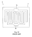
- Fig. 12 shows a SAW filter 1 in a plan view as an example of a conventional surface acoustic wave device (hereinafter, referred to also as a SAW device).
- the SAW filter 1 includes a piezoelectric substrate 2 and a pair of interdigital transducers 3a and 3b (hereinafter, referred to also as IDT electrodes) formed on the substrate 2.
- the substrate 2 is formed of LiTaO 3 , LiNbO 3 or the like.
- the substrate 2 has a pyroelectric property
- a change in temperature in an assembly process or a change in temperature when used as a device causes non-uniformity in electric charge distribution on the surface of the substrate 2.
- a potential difference is generated between the IDT electrodes 3a and 3b so that discharge occurs between the electrodes.
- the discharge between the electrodes causes melting and cutting-off of the electrodes, resulting in deterioration or shift of the characteristics of the filter.
- a first method is to connect the two IDT electrodes by a fine metal electrode (see JP 3-29407A).
- this metal electrode is fine, the electric connection is easily broken, for example by heat. Thus, this method cannot provide a reliable filter.
- a second method is to form a thin film having a predetermined resistivity that covers the IDT electrodes (see JP1-106611A, JP10-303681A, and JP11-74750A).
- a process for forming the thin film is required.
- a third method is to treat the substrate with heat in a reducing gas to reduce the surface resistance, and then to form IDT electrodes (see SURFACE
- the SAW filter obtained by the third method has a problem in that insertion loss of high frequency characteristics is increased. It is believed that this is caused by lattice defects generated significantly deep in the substrate when the substrate is treated with heat in a reducing gas, which affects the propagation of the surface acoustic wave energy.
- a first surface acoustic wave device of the present invention includes a piezoelectric substrate, a first interdigital transducer and a second interdigital transducer formed on the substrate so that the first and second interdigital transducers are opposed to each other.
- the substrate includes a doping region that is doped with a substance in at least one form selected from the group consisting of atoms, molecules and clusters in a surface between the first and second interdigital transducers. This substance may be in the form of ions or radicals. This invention is based on the discovery that when the doping region is formed between the electrodes, discharge between the electrodes can be suppressed.
- the doping region has a lower resistance than that of the substrate that is not doped.
- the SAW device when a potential difference is generated between the first IDT electrode and the second IDT electrode, electric charges are transferred via the doping region so that the potential difference is eliminated. Therefore, according to the above-described SAW device, discharge between the IDT electrodes can be suppressed.
- the doping region is formed only in the surface of the substrate. Therefore, the SAW device has good characteristics for propagation of surface acoustic waves.
- the depth of the doping region may be not more than 50nm. Most of the surface acoustic waves that propagate on the surface of the SAW device propagate in a region in a depth up to about 1/4 of the wavelength of the surface acoustic wave from the surface of the substrate. In the case of a SAW device with a 2GHz band using LiNbO 3 , the surface acoustic waves propagate in a region in a depth up to about 0.5 ⁇ m from the surface of the substrate.
- This embodiment can provide a SAW device having particularly good characteristics for propagation of the surface acoustic waves, because the doping region is sufficiently thin relative to the region for propagation.
- the doping region has a lower resistance than that of an inner portion of the substrate.
- the sheet resistance of the doping region may be in a range from 10 8 ⁇ / ⁇ to 10 15 ⁇ / ⁇ . This embodiment particularly can suppress discharge between the IDT electrodes.
- the substance may be a substance obtained by ionizing at least one selected from the group consisting of a reducing gas, silane, nitrogen, oxygen, argon, silicon, arsenic, boron, phosphorus, tin, indium, chromium, tantalum, molybdenum, germanium, and nickel.
- a reducing gas silane, nitrogen, oxygen, argon, silicon, arsenic, boron, phosphorus, tin, indium, chromium, tantalum, molybdenum, germanium, and nickel.
- the first and second interdigital transducers may be provided with an insulating layer on surfaces thereof.
- "on a surface” includes “in a surface”, and forming on a surface includes forming by doping in a surface.
- This embodiment can prevent the short-circuit of the electrodes caused by conductive particles. Moreover, this embodiment can prevent corrosion of the electrodes, and this effect is particularly large when the electrodes comprise aluminum.
- the insulating layer is formed by doping a metal with impurities, the doping of impurities reduces the grain size of crystals on the surface of the electrodes, so that movement of atoms of Al or the like can be inhibited. Therefore, in this case, migration in the electrodes can be suppressed.
- the average thickness of the insulating layer may be in a range from 2nm to 500nm, and the resistivity of the insulating layer may be not less than 10 6 ⁇ cm.
- An average thickness of the layer of 2nm or more can suppress the short-circuit between the electrodes and corrosion of the electrodes.
- An average thickness of the layer of 500nm or less can prevent deterioration of the characteristics of the surface acoustic wave device.
- a resistivity of the insulating layer of not less than 10 6 ⁇ cm particularly can suppress the short-circuit between the electrodes.
- the insulating layer may be made of a metal nitride or a metal oxide. This embodiment can prevent not only pyroelectricity breakdown of the electrodes, but also corrosion of the electrodes and the short-circuit between the electrodes.
- a method for producing a surface acoustic wave device includes (a) forming a first interdigital transducer and a second interdigital transducer on a piezoelectric substrate so that the first and second interdigital transducers are opposed to each other; and (b) forming a doping region in a surface of the substrate between the first and second interdigital transducers by doping the surface of the substrate with a substance in at least one form selected from the group consisting of atoms, molecules and clusters before or after the process (a).
- This substance may be in the form of ions or radicals.
- the substrate may be doped with the substance in a depth of not more than 50nm from the surface thereof.
- This embodiment allows the doping region to be formed in a depth of not more than 50nm.
- the doping region has a lower resistance than that of an inner portion of the substrate.
- the sheet resistance of the doping region may be in a range from 10 8 ⁇ / ⁇ to 10 15 ⁇ / ⁇ .
- the substrate may be doped with the substance in ionized form.
- the dose of the substance may be in a range from 1 ⁇ 10 13 ions/cm 2 to 1 ⁇ 10 17 ions/cm 2 .
- a dose of not less than 1 ⁇ 10 13 ions/cm 2 can form a doping region having a preferable sheet resistance.
- a dose of not more than 1 ⁇ 10 17 ions/cm 2 particularly can suppress the deterioration of the characteristics of the SAW device.
- the substrate may be doped with the substance in an energy of 0.01keV to 10keV.
- This embodiment allows the depth of the doping region to be 50nm or less, and particularly can suppress the deterioration of the characteristics of the SAW device.
- the substance may be a substance obtained by ionizing at least one selected from the group consisting of a reducing gas, silane, nitrogen, oxygen, argon, silicon, arsenic, boron, phosphorus, tin, indium, chromium, tantalum, molybdenum, germanium, and nickel.
- the substrate may be doped with the substance by at least one technique selected from the group consisting of ion implantation, ion doping, plasma doping, laser doping and vapor phase doping.
- This embodiment can form a doping layer simply and controllably.
- the above-described method for producing a surface acoustic wave device further may include (c) forming an insulating layer in surfaces of the first and second interdigital transducers by doping the surfaces of the first and second interdigital transducers with impurities after the process (a).
- This embodiment can prevent the short-circuit between the electrodes caused by conductive particles.
- the impurities may be the same substance as said substance, and the process (c) may be performed at the same time as the process (b).
- This embodiment can form the doping region and the insulating layer at one time of doping.
- the impurities may be oxygen or nitrogen.
- the average thickness of the insulating layer may be in a range from 2nm to 500nm, and the resistivity of the insulating layer may be not less than 10 6 ⁇ cm.
- a second surface acoustic wave device of the present invention includes a piezoelectric substrate, a first interdigital transducer and a second interdigital transducer formed on the substrate so that the first and second interdigital transducers are opposed to each other, wherein the substrate includes a plurality of conductive regions that spaced apart from each other on a surface thereof between the first and second interdigital transducers, and a tunnel current flows between the first and second interdigital transducers via the conductive regions.
- the SAW device of the present invention and the method for producing a SAW device of the present invention easily provide a surface acoustic wave device in which discharge between the IDT electrodes hardly occurs and that has good characteristics for SAW propagation.
- the present invention is useful for various SAW devices such as ladder type or traveling-wave type SAW filters or SAW resonators.
- Fig. 1A is a plan view of an example of a SAW device of the present invention.
- Fig. 1B is a cross-sectional view of the example of the SAW device of the present invention.
- Fig. 2 is a cross-sectional view of another example of a SAW device of the present invention.
- Figs. 3A to 3C are views showing a process sequence of an example of a method for producing a SAW device of the present invention.
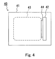
- Fig. 4 is a schematic view showing an example of a plasma doping apparatus used in a method for producing a SAW device of the present invention.
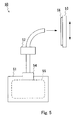
- Fig. 5 is a schematic view showing an example of an ion implanting apparatus used in a method for producing a SAW device of the present invention.
- Figs. 6A to 6D are views showing a process sequence of another example of a method for producing a SAW device of the present invention.
- Figs. 7A to 7C are views showing a process sequence of yet another example of a method for producing a SAW device of the present invention.
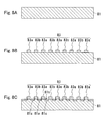
- Figs. 8A to 8C are views showing a process sequence of still another example of a method for producing a SAW device of the present invention.
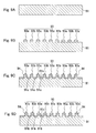
- Figs. 9A to 9D are views showing a process sequence of another example of a method for producing a SAW device of the present invention.
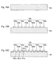
- Figs. 10A to 10C are views showing a process sequence of yet another example of a method for producing a SAW device of the present invention.
- Fig. 11A is a cross-sectional view of yet another example of a SAW device of the present invention.
- Fig. 11B is a cross-sectional view of still another example of a SAW device of the present invention.
- Fig. 12 is a plan view of an example of a conventional SAW device.
- Fig. 1A is a plan view of a SAW device 10 of Embodiment 1.
- Fig. 1B is a cross-sectional view of the SAW device 10 taken along line X-X.
- the SAW device 10 includes a substrate 11, a pair of IDT electrodes 12 formed on the substrate 11, and reflectors 13 formed on the substrate 11.
- the pair of IDT electrodes 12 includes a first IDT electrode 12a and a second IDT electrode 12b.
- the substrate 11 includes a doping region 11a in a substrate surface 11s between the first IDT electrode 12a and the second IDT electrode 12b and between the IDT electrodes 12 and the reflectors 13.
- the SAW device 10 includes electric wires or pad electrodes, if necessary.
- the SAW device of the present invention may include a plurality of sets of IDT electrodes on the substrate.
- a substrate having a piezoelectric property and a pyroelectric property can be used as the substrate 11.
- a substrate made of LiTaO 3 or LiNbO 3 can be used. More specifically, a 64° Y-cut X-propagating LiNbO 3 substrate or a 39° Y-cut X-propagating LiTaO 3 substrate can be used.
- the doping region 11a in the substrate 11 is doped with a substance in at least one form selected from the group consisting of atoms, molecules and clusters.
- the substance for doping may be in the form of ions or radicals.
- the doping region 11a has a lower resistance than that of the inner portion of the substrate. In other words, the doping region 11a has a lower resistance than that of the substrate that is not doped.
- the resistivity and the depth of the doping region 11a are set to such values that can suppress discharge between the first IDT electrode 12a and the second IDT electrode 12b.
- the depth of the doping region 11a from the substrate surface 11s is 50nm or less, and more preferably is 10nm or less.
- the sheet resistance of the substrate surface 11s between the first and the second IDT electrodes 12a and 12b namely, the sheet resistance of the doping region 11a, preferably is in the range from 10 8 ⁇ / ⁇ to 10 15 ⁇ / ⁇ , more preferably in the range from 10 12 ⁇ / ⁇ to 10 14 ⁇ / ⁇ .
- the sheet resistance is measured in an electric field of 10 5 V/cm or less, which also applies to the following).
- a sheet resistance of 10 8 ⁇ / ⁇ or more can suppress the deterioration of the characteristics of the SAW device 10 such as insertion loss.
- Discharge between the IDT electrodes 12a and 12b depends on the temperature, the rate of temperature change of the substrate 11, the state of the gas in contact with the surface of the substrate 11, and the state of light with which the substrate is irradiated during the production process or in use. Moreover, the discharge depends on the distance between the two adjacent electrodes, the shape of the ends of the electrodes, and the area of the electrodes. Therefore, the sheet resistance of the doping region 11a is adjusted in view of the aforementioned conditions. The sheet resistance can be adjusted by changing the type or the amount of the substance with which the substrate is doped.
- the sheet resistance of a LiTaO 3 substrate or a LiNbO 3 substrate is about 10 15 ⁇ / ⁇ or more in an average electric field of 10 5 V/cm or less when the substrate is not doped.
- the sheet resistance of the surface of the doping region 11a has a lower resistance than that of the inner portion of the substrate.
- the substance with which the doping region 11a is doped for example, a substance obtained by ionizing at least one ion species selected from the group consisting of a reducing gas, silane, nitrogen, oxygen, argon, silicon, arsenic, boron, phosphorus, tin, indium, chromium, tantalum, molybdenum, germanium, and nickel can be used.
- a reducing gas for example, hydrogen, carbon monoxide, nitrogen monoxide or the like can be used.
- nitrogen it is most preferable to use nitrogen as the ion species, because nitrogen causes only a small level of deterioration of the characteristics for propagation of surface acoustic waves.
- the reducing gas As the ion species, oxygen defects can be formed effectively on the surface of the substrate made of an oxide. More specifically, such oxygen defects act as a donor so that the surface resistance of the doping region 11a can be reduced. Furthermore, when the substrate is made of LiTaO 3 , it also is advantageous to dope the substrate with carbon or nitrogen. In this case, tantalum carbide or tantalum nitride, which is a compound having a conductivity higher than that of LiTaO 3 , is formed, so that the surface resistance of the doping region 11a is reduced.
- lattice defects can be formed in the substrate surface. It is believed that such lattice defects act as a trap center, a donor, or an acceptor, so that the surface resistance of the doping region 11a is reduced.
- the accelerating energy for doping can be in the range from 0.01keV to 10keV.
- the dose in this case can be any amount, as long as the sheet resistance as described above is attained.
- a dose of 1 ⁇ 10 13 ions/cm 2 to 1 ⁇ 10 17 ions/cm 2 can be used.
- Figs. 1A and 1B show the IDT electrodes 12 only schematically, and IDT electrodes 12 for practical use are provided with more branches, for example, 100 to 500 branches.
- the IDT electrodes are made ofAl, anAl alloy or other metals.
- As an Al alloy for example, an Al-Cu alloy or an Al-Cu-Si alloy can be used.
- the IDT electrodes 12 can be formed with a single metal film or a plurality of metal films.
- the shortest distance between the first IDT electrode 12a and the second IDT electrode 12b depends on the speed of sound as determined by the frequency and the substrate material. For example, the shortest distance therebetween is in the range from 0.01 ⁇ m to 100 ⁇ m.
- the reflectors 13 are formed to suppress leakage of the surface acoustic waves from the IDT electrodes 12.
- the reflectors are formed in such a manner that the IDT electrodes 12 are interposed between the reflectors.
- the reflectors can be made of the same material as used for the IDT electrodes 12.
- the SAW device 10 can be used as a single device or in connection with a package, which encloses the SAW device.
- the SAW device 10 can be connected to the package by wire bonding or flip chip bonding.
- Figs. 1A and 1B show the SAW device where the doping region 11a is formed only between adjacent electrodes (including the IDT electrodes and the reflectors) on the substrate 11. However, as shown in Fig. 6D, the doping region can be formed in the entire surface of the substrate on the side where the IDT electrodes are formed.
- the SAW device of the present invention may include an insulating layer on the surface of the IDT electrodes.
- Fig. 2 shows an example of such a SAW device 20 in section.
- the SAW device 20 is different from the SAW device 10 only in the IDT electrodes and the reflectors, so that duplicate description will be omitted.
- the SAW device 20 includes IDT electrodes 22 and reflectors 23 formed on the substrate 11.
- the IDT electrodes 22 include a first IDT electrode 22a and a second IDT electrode 22b.
- the first IDT electrode 22a and the second IDT electrode 22b are the first IDT electrode 12a and the second IDT electrode 12b provided with an insulating layer 24 on the surfaces thereof, respectively.
- the IDT electrodes 22 are provided with the insulating layer 24 on the surfaces thereof.
- the reflectors 23 are provided with an insulating layer 25 on the surface thereof.
- the resistivity of the insulating layers 24 and 25 is, for example, 10 6 ⁇ cm or more.
- the insulating layers 24 and 25 are made of, for example a metal nitride or a metal oxide.
- the insulating layers 24 and 25 aluminum nitride or aluminum oxide can be used for the insulating layers 24 and 25.
- the thickness of the insulating layers 24 and 25 preferably is 2nm to 500nm, more preferably 2nm to 10nm.
- the insulating layer 24 can be formed by doping the surface of the IDT electrodes made of a metal with impurities that form an insulator with the metal.
- the insulating layer 25 can be formed by doping the reflectors made of a metal with impurities. Examples of the impurities include nitrogen and oxygen. Doping of the impurities can be performed in the same manner in which the doping region 11a is formed, which will be described in Embodiment 2.
- the SAW device of Embodiment 1 can be produced in the same manner as described in Embodiment 2.
- the doping region 11a is formed in the substrate surface 11s. Therefore, this SAW device can prevent discharge between the electrodes from occurring during and after production. Furthermore, since the doping region 11a is formed only in the surface of the substrate 11, the SAW device has good characteristics for propagation of surface acoustic waves.
- the SAW device of Embodiment 1 can be miniaturized, because it is unnecessary to form metal electrodes for connection, unlike conventional SAW devices where the IDT electrodes are connected by metal electrodes.
- Embodiment 2 a method of the present invention for producing a SAW device will be described.
- the same components as those described in Embodiment 1 bear the same reference numerals, and duplicate description will be omitted.
- the method of Embodiment 2 includes (a) forming a first IDT electrode and a second IDT electrode on a piezoelectric substrate in such a manner that the first IDT electrode and the second IDT electrode are opposed to each other.
- this process may be referred to as process (a).
- this method includes (b) forming a doping region in a surface of the substrate by doping the surface of the substrate between the first IDT electrode and the second IDT electrode with a substance in at least one form selected from the group consisting of atoms, molecules and clusters before or after the process (a).
- this process may be referred to as process (b).
- the substance with which the substrate is doped may be in the form of ions or radicals.
- a pair of IDT electrodes 12 and reflectors 13 are formed on a substrate 31.
- a first IDT electrode 12a and a second IDT electrode 12b are opposed to each other.
- the substrate 31 becomes the substrate 11.
- the IDT electrodes 12 can be formed by photolitho-etching or lift-off technology.
- the doping region 11a is formed in the substrate surface 11s at least between the first IDT electrode 12a and the second IDT electrode 12b and between the IDT electrodes 12 and the reflectors 13.
- the doping region 11a can be formed by doping the substrate surface 11s with a substance in at least one form selected from the group consisting of atoms, molecules and clusters (hereinafter, the substance may be referred to as an additive substance).
- the substance may be referred to as an additive substance.
- the substrate surface 11s It is preferable to dope the substrate surface 11s with the additive substance in a depth of not more than 50nm (more preferably, not more than 10nm) from the substrate surface 11s. In other words, it is preferable that the depth of the doping region 11a is not more than 50nm.
- the doping region 11a has a lower resistance than that of the inner portion of the substrate.
- the sheet resistance of the substrate surface 11s, namely, the doping region 11a preferably is in the range from 10 8 ⁇ / ⁇ to 10 15 ⁇ / ⁇ , more preferably in the range from 10 12 ⁇ / ⁇ to 10 14 ⁇ / ⁇ .
- the additive substance can be used in the form of ions for doping.
- the dose of ions can be any amount, as long as the sheet resistance as described above is attained.
- a dose of 1 ⁇ 10 13 ions/cm 2 to 1 ⁇ 10 17 ions/cm 2 can be used.
- the accelerating energy for the doping can be in the range from 0.01keV to 10keV.
- the additive substance for example, a substance obtained by ionizing at least one ion species selected from the group consisting of a reducing gas, silane, nitrogen, oxygen, argon, silicon, arsenic, boron, phosphorus, tin, indium, Cr, Ta, Mo, Ge, and Ni can be used.
- a reducing gas for example, hydrogen, carbon monoxide, nitrogen monoxide or the like can be used.
- nitrogen radicals or oxygen radicals can be used as atoms with which the substrate is doped.
- a substrate made of an oxide such as LiTaO 3 or LiNbO 3 it is advantageous to use the reducing gas as the ion species. Furthermore, it also is advantageous to use a neutral gas such as Ar or nitrogen, gas having a relatively large mass, or metal ions.
- the doping of the additive substance can be performed by at least one technique selected from the group consisting of ion implantation, ion doping, plasma doping, laser doping and vapor phase doping.
- ion implantation technique doping is performed by accelerating ions generated in plasma and separating the ions by mass.
- ion doping technique doping is performed by accelerating ions generated in plasma without separating the ions by mass.
- plasma doping doping is performed by exposing the substrate to plasma.
- the laser doping technique doping is performed by irradiating the surface of the substrate with a laser while exposing the substrate to a gas comprising atoms with which the substrate is to be doped.
- doping is performed by exposing the substrate to a gas comprising atoms with which the substrate is to be doped and then treating the substrate with heat.
- plasma doping is preferable in that it is a low-temperature and low energy process, and therefore a shallow doping region can be formed easily.
- Fig. 4 schematically shows the structure of an example of a plasma doping apparatus.
- the doping apparatus 40 includes a chamber 41 and a substrate stage 42 placed in the chamber 41.
- a tube for gas supply (not shown) and a tube for exhaustion (not shown) are connected to the chamber 41.
- Plasma 43 is formed immediately above the substrate stage 42.
- a substrate 44 on the substrate stage 42 is exposed to the plasma 43 and doped with radicals or ions in the plasma 43.
- the plasma 43 is formed by RF electrodes (not shown) provided in the chamber 41.
- Fig. 5 schematically shows the structure of an example of an ion implanting apparatus.
- the ion implanting apparatus 50 includes a chamber 51, a mass separator 52 connected to the chamber 51 and a substrate stage 53.
- a tube for gas supply (not shown) and a tube for exhaustion (not shown) are connected to the chamber 51. Outside the chamber 51, there is an extracted electrode 54 for ions.
- the chamber 51, the mass separator 52 and the substrate stage 53 are placed substantially under vacuum.
- the substrate stage 53 is movable.
- a substrate 56 is placed on the substrate stage 53.
- Plasma 55 is formed in the chamber 51.
- Ions generated in the plasma 55 are extracted from the chamber 51 by the extracted electrode 54, accelerated by a pre-accelerator (not shown), separated by the mass separator 52, and accelerated or decelerated by post-accelerator (not shown), if necessary, and then implanted on the substrate 56.
- the plasma 55 is formed by RF electrodes provided in the chamber 51.
- the SAW device 10 can be mounted in the manner shown in Fig. 3C.
- the substrate 11 is cut into individual elements, and then an element is fixed to a mounting substrate 33 with a resin 32. Then, wire bonding is performed using a bonding wire 34, and seam welding is performed in a nitrogen atmosphere. In this mounting process, the substrate 11 is heated. However, discharge can be prevented because the substrate 11 is provided with the doping region 11a.
- the doping region may be etched during a process for forming the IDT electrodes 12 (e.g., dry etching). For this reason, in this case, the conditions for the process for forming the IDT electrodes are restricted.
- the process (b) is performed after the process (a), such restrictions can be eliminated.
- the process (b) is performed after the process (a)
- equipment or material can be shared with an apparatus used in another process.
- the apparatus used in another process include a sputtering cleaning apparatus, a dry etching apparatus, and a resist ashing apparatus.
- the equipment that can be shared include a chamber, an ionizer, an exhausting apparatus and a gas tube.
- doping of the ions can be performed using a dry etching apparatus.
- a dry etching process and the plasma doping process can be performed successively in the same chamber or different chambers. In this manner, the SAW device can be produced with good production yield and reliability by performing the process (b) after process (a).
- the method of the present invention may include a process for forming the insulating layers 24 and 25 by doping the surfaces of the IDT electrodes 12 and the reflectors 13 with impurities after the process (a).
- this process may be referred to as process (c).
- the insulating layers 24 and 25 can be formed after removing a resist on the electrodes. More specifically, the insulating layers 24 and 25 can be formed before the process (b), at the same time as the process (b), or after the process (b).
- the processes (b) and (c) can be performed at the same time by one doping process. More specifically, when the IDT electrodes 12 and the reflectors 13 are made of a metal comprising Al, it is preferable to dope the substrate 31, the IDT electrodes 12 and the reflectors 13 with nitrogen or oxygen. In this case, the insulating layers are formed most efficiently by using nitrogen radials and oxygen radicals for doping.
- the method of Embodiment 2 can produce a SAW device in which discharge hardly occurs between the IDT electrodes and that has good characteristics for propagation of surface acoustic waves. Moreover, the method of Embodiment 2 can suppress discharge during production processes, so that the SAW device can be produced in good yield.
- Example 1 to 4 are examples that can be carried out, and Example 5 is an example that was actually carried out.
- a reflector is not formed. However, a reflector can be formed.
- Example 1 an example of a method for producing a SAW device of the present invention will be described.
- Figs. 6A to 6D show a production process sequence of Example 1.
- a substrate 61 made of LiTaO 3 is prepared, and the surface thereof is washed.
- a doping region 61a having a sheet resistance in the range from 10 8 ⁇ / ⁇ to 10 15 ⁇ / ⁇ is formed in the substrate 61.
- the doping region 61a can be formed by doping the substrate 61 with boron ions by plasma doping.
- the doping of boron ions can be performed under the conditions of an implantation energy of 700eV and a dose of 1 ⁇ 10 16 ions/cm 2 .
- a metal film 62 (a thickness of 800nm) made of aluminum is formed over the substrate 61 by sputtering.
- IDT electrodes 63a and 63b are formed by removing unnecessary portions in the metal film 62.
- the IDT electrodes are formed in the following manner. First, a resist film (a thickness of 1 ⁇ m) is formed on the metal film 62, and a predetermined pattern is formed by photolithography. Then, unnecessary portions in the metal film 62 are removed by dry-etching using a chlorine-based gas. Finally, the resist film is ashed with oxygen plasma. Thus, the formation of the IDT electrodes is completed.
- the mounting of the SAW device is performed. Specifically, first, the substrate 61 is diced and cut into individual elements. Next, die bonding is performed at 180°C with a silicon resin to bond the substrate 61 to a mounting substrate. Then, wire bonding is performed to the IDT electrodes 63a and 63b. Finally, seam welding is performed in a nitrogen atmosphere.
- ions are implanted before the IDT electrodes are formed. According to the SAW device produced by the method of Example 1, discharge between the electrodes can be prevented.
- a nitrogen gas comprising 0.1vol% to 5vol% of hydrogen, or a helium gas comprising 0.1vol% to 5vol% of hydrogen may be used.
- plasma doping can be performed under the conditions of an implanting energy of 700eV and a dose of 1 ⁇ 10 16 ions/cm 2 .
- Example 2 another example of a method for producing a SAW device of the present invention will be described.
- Figs. 7A to 7C show a production process sequence of Example 2.
- a substrate 71 made of LiTaO 3 is prepared, and the surface thereof is washed.
- IDT electrodes 73 including IDT electrodes 73a and 73b are formed.
- the IDT electrodes are formed in the following manner. First, a metal film (a thickness of 200nm) made of aluminum is formed on a substrate 71, and a resist film (a thickness of 1 ⁇ m) having a predetermined pattern is formed on the metal film. Then, unnecessary portions in the metal film are removed by dry-etching using a chlorine-based gas. Finally, the resist film is ashed with oxygen plasma. Thus, the formation of the IDT electrodes is completed.
- an insulating layer 74 is formed on the IDT electrodes 73a and 73b.
- a doping region 71a having a sheet resistance in the range from 10 8 ⁇ / ⁇ to 10 15 ⁇ / ⁇ is formed in a substrate surface 71s between the IDT electrodes 73a and 73b.
- the insulating layer 74 and the doping region 71a can be formed by doping the substrate 71 with oxygen ions by plasma doping.
- the doping of oxygen ions can be performed under the conditions of an implantation energy of 5000eV and a dose of 1 ⁇ 10 17 ions/cm 2 .
- ions are implanted after the IDT electrodes are formed and the resist film is removed.
- discharge between the electrodes can be prevented.
- the method of Example 2 can suppress a short-circuit generated by conductive particles adhering during the production process.
- corrosion of the electrodes and stress migration can be suppressed.
- Example 3 another example of a method for producing a SAW device of the present invention will be described.
- Figs. 8A to 8C show a production process sequence of Example 3.
- a substrate 81 made of LiTaO 3 is prepared, and the surface thereof is washed.
- IDT electrodes 83 including IDT electrodes 83a and 83b are formed.
- the IDT electrodes are formed in the same manner as in Example 2.
- a doping region 81a having a sheet resistance in the range from 10 8 ⁇ / ⁇ to 10 15 ⁇ / ⁇ is formed in a substrate surface 81s between the IDS electrodes 83a and 83b.
- the doping region 81a can be formed by doping the substrate 81 with boron ions by plasma doping.
- the doping of boron ions can be performed under the conditions of an implantation energy of 700eV and a dose of 1 ⁇ 10 16 ions/cm 2 .
- the boron ions are implanted also in the IDT electrodes. However, this does not affect the electric characteristics of the SAW device.
- ions are implanted after the IDT electrodes are formed. According to the SAW device produced by the method of Example 3, discharge between the electrodes can be prevented.
- a nitrogen gas comprising 0.1vol% to 5vol% of hydrogen, or a helium gas comprising 0.1vol% to 5vol% of hydrogen may be used.
- plasma doping can be performed under the conditions of an implanting energy of 700eV and a dose of 1 ⁇ 10 16 ions/cm 2 .
- Example 4 another example of a method for producing a SAW device of the present invention will be described.
- Figs. 9A to 9D show a production process sequence of Example 4.
- a substrate 91 made of LiTaO 3 is prepared, and the surface thereof is washed.
- IDT electrodes 93 including IDT electrodes 93a and 93b are formed.
- the IDT electrodes are formed in the same manner as in Example 2.
- an insulating layer 94 is formed on the surfaces of the IDT electrodes 93a and 93b.
- a doping region 91a is formed in a substrate surface 91s between the IDS electrodes 93a and 93b.
- the insulating layer 94 and the doping region 91a can be formed by plasma-doping of oxygen ions.
- the doping of oxygen ions can be performed under the conditions of implantation energy: 5000eV and dose: 1 x 10 17 ions/cm 2 .
- the doping region 91a is doped with boron ions by plasma-doping, so that a doping region 91b having a lower resistance than that of the doping region 91a is formed.
- the sheet resistance of the doping region 91b is in the range from 10 8 ⁇ / ⁇ to 10 15 ⁇ / ⁇ .
- the doping of boron ions can be performed under the conditions of an implantation energy of 700eV and a dose of 1 ⁇ 10 16 ions/cm 2 .
- Example 4 As described above, in the method of Example 4, the same effects provided by the method of Example 2 can be obtained. Moreover, the method of Example 4 allows the sheet resistance of the doping region 91b to be controlled easily.
- Example 5 an example of a SAW device actually produced by the method of the present invention will be described.
- Figs. 10A to 10C show a production process sequence of the method of Example 5.
- a substrate 101 made of LiTaO 3 was prepared, and the surface thereof was washed.
- IDT electrodes 103 including IDT electrodes 103a and 103b were formed.
- a doping region 101a was formed in a substrate surface 101s between the IDT electrodes 103a and 103b.
- the doping region 101a can be formed by ICP plasma-doping of nitrogen ions.
- three types of SAW devices were formed under varied doping conditions. These three types of SAW devices were subjected to a heating test and evaluation of RF characteristics. In addition, the same tests were conducted with respect to a SAW device that was not doped with nitrogen ions as a comparative example. Table 1 shows the doping conditions and the results of the tests with respect to the above samples.
- the heating test was performed by heating 100 devices of each type of sample to 50°C with a hot plate and measuring the number of devices that was damaged by discharge.
- Table 1 the number of devices that was damaged of the 100 devices is shown.
- the RF characteristics the mean frequency and the frequency band were measured using a network analyzer.
- Fig. 11A is a cross-sectional view of a SAW device 200 of a first example.
- Fig. 11B is a cross sectional view of a SAW device 210 of a second example.
- the SAW device 200 includes a substrate 201 made of piezoelectric material and IDT electrodes 202 formed on the substrate 201.
- the IDT electrodes 202 include pairs of IDT electrodes 202a and 202b that are opposed to each other.
- the IDT electrodes 202 are the same as the IDT electrodes 12 described in Embodiment 1.
- a plurality of dotted metals 203 are formed on a substrate surface at least between the IDT electrodes 202a and 202b.
- the metals 203 are separated by a distance that allows a tunnel current to flow between the adjacent metals 203. More specifically, the metals 203 are formed on the substrate at a density of 10 metals / ⁇ m 2 or more.
- the metals can be formed, for example by performing a sensitizing treatment and an activating treatment, which are pre-treatments of electroless plating. More specifically, as the sensitizing treatment, the substrate 201 is treated with a treatment aqueous solution (SnCl 2 : 10g /l, HCl : 40ml/l, 323K).
- the substrate 201 is treated with a treatment aqueous solution (PdCl 2 : 0.2g /l, HCl : 20ml/l, 323K).
- a treatment aqueous solution PdCl 2 : 0.2g /l, HCl : 20ml/l, 323K.
- the SAW device 200 when a high voltage is applied across the electrodes, a tunnel current flows via the metals 203, so that discharge between the electrodes can be prevented. Therefore, according to the SAW device 200, discharge breakdown can be prevented during and after the production process. Furthermore, since the metals 203 are insulated, the characteristics of the device are not adversely affected. Furthermore, the SAW device 200 is not affected by environmental changes such as repetition stress and has high reliability.
- the dotted metals 203 can be formed by other methods such as utilizing an early state (island-shaped metal) in metal deposition.
- the SAW device 210 includes a substrate 211 made of piezoelectric material and IDT electrodes 212 formed on the substrate 211.
- the IDT electrodes 212 are the same as the IDT electrodes 12 described in Embodiment 1.
- the substrate 211 is provided with doping regions 211a (Fig. 11B) formed in stripes.
- the doping regions may be formed in a mesh.
- the doping region 211a is formed by doping the substrate with a substance in at least one form selected from the group consisting of atoms, molecules and clusters.
- the SAW device 210 when a high voltage is applied across the electrodes, a tunnel current flows via the doping regions 211a, so that discharge between the electrodes can be prevented. Therefore, according to the SAW device 210, the same effects provided by the SAW device 200 can be obtained. Furthermore, since the doping regions 211a are formed in stripes in the SAW device 210, the direct current resistance is low and the high frequency resistance is high. For this reason, discharge between the electrodes can be prevented, and the same characteristics of a regular SAW device can be obtained.
Landscapes
- Physics & Mathematics (AREA)
- Acoustics & Sound (AREA)
- Engineering & Computer Science (AREA)
- Manufacturing & Machinery (AREA)
- Surface Acoustic Wave Elements And Circuit Networks Thereof (AREA)
Applications Claiming Priority (2)
| Application Number | Priority Date | Filing Date | Title |
|---|---|---|---|
| JP27868399 | 1999-09-30 | ||
| JP27868399 | 1999-09-30 |
Publications (2)
| Publication Number | Publication Date |
|---|---|
| EP1089431A2 true EP1089431A2 (fr) | 2001-04-04 |
| EP1089431A3 EP1089431A3 (fr) | 2003-12-10 |
Family
ID=17600727
Family Applications (1)
| Application Number | Title | Priority Date | Filing Date |
|---|---|---|---|
| EP00308648A Withdrawn EP1089431A3 (fr) | 1999-09-30 | 2000-10-02 | Dispositif à ondes acoustiques de surface et procédé de fabrication du même |
Country Status (2)
| Country | Link |
|---|---|
| US (1) | US6984540B2 (fr) |
| EP (1) | EP1089431A3 (fr) |
Cited By (2)
| Publication number | Priority date | Publication date | Assignee | Title |
|---|---|---|---|---|
| WO2003065577A1 (fr) * | 2002-02-01 | 2003-08-07 | Unaxis Balzers Limited | Dispositif de traitement des ondes acoustiques de surface presentant une performance amelioree et procede de fabrication dudit dispositif |
| US8957565B2 (en) | 2010-11-10 | 2015-02-17 | Murata Manufacturing Co., Ltd. | Acoustic wave device and method for manufacturing the same |
Families Citing this family (8)
| Publication number | Priority date | Publication date | Assignee | Title |
|---|---|---|---|---|
| US7425881B2 (en) * | 2004-03-18 | 2008-09-16 | Murata Manufacturing Co., Ltd. | Surface acoustic wave device and method that prevents restoration of a pyroelectric effect |
| JP6344466B2 (ja) * | 2014-03-31 | 2018-06-20 | 株式会社村田製作所 | 弾性波装置 |
| US9906206B2 (en) * | 2016-06-20 | 2018-02-27 | Ishiang Shih | Tunable surface acoustic wave resonators and filters |
| WO2019142483A1 (fr) | 2018-01-22 | 2019-07-25 | 日本碍子株式会社 | Ensemble de substrat de matériau piézoélectrique et de substrat de support, et procédé de fabrication associé |
| JP2020145567A (ja) * | 2019-03-06 | 2020-09-10 | 株式会社村田製作所 | 弾性波装置 |
| CN116057835A (zh) * | 2020-09-09 | 2023-05-02 | 株式会社村田制作所 | 弹性波装置 |
| CN113489471B (zh) * | 2021-07-12 | 2023-11-17 | 无锡市好达电子股份有限公司 | 一种低损耗的声表面波装置 |
| CN120729228B (zh) * | 2025-08-18 | 2025-11-28 | 天通瑞宏科技有限公司 | 一种声表面波谐振器及滤波器 |
Family Cites Families (12)
| Publication number | Priority date | Publication date | Assignee | Title |
|---|---|---|---|---|
| GB1513466A (en) | 1975-09-19 | 1978-06-07 | Mullard Ltd | Acoustic surface wave devices |
| JPS59124306A (ja) * | 1982-12-29 | 1984-07-18 | Canon Inc | 光集積回路素子およびその作製方法 |
| JPH01106611A (ja) | 1987-10-20 | 1989-04-24 | Fujitsu Ltd | 圧電素子 |
| JPH0329407A (ja) | 1989-06-26 | 1991-02-07 | Mitsubishi Electric Corp | 弾性表面波発性装置 |
| JP3163606B2 (ja) | 1993-01-29 | 2001-05-08 | 住友電気工業株式会社 | 表面弾性波素子 |
| FR2714200B1 (fr) * | 1993-11-25 | 1996-12-27 | Fujitsu Ltd | Dispositif à onde acoustique de surface et son procédé de fabrication. |
| WO1996004713A1 (fr) * | 1994-08-05 | 1996-02-15 | Japan Energy Corporation | Dispositif a ondes acoustiques de surface et procede de production |
| JPH09199974A (ja) | 1996-01-19 | 1997-07-31 | Nec Corp | 弾性表面波装置 |
| JPH10303681A (ja) | 1997-04-24 | 1998-11-13 | Kyocera Corp | 弾性表面波装置 |
| FR2764440B1 (fr) | 1997-06-10 | 2001-11-09 | Thomson Csf | Composant a ondes acoustiques de surface avec suppression de perturbation pyroelectrique |
| EP0893515B1 (fr) | 1997-07-25 | 2003-11-26 | Crystal Technology, Inc. | Cristaux pretraites de niobate de lithium et de tantalate de lithium et methodes pour leur preparation |
| JPH1174750A (ja) * | 1997-08-29 | 1999-03-16 | Kyocera Corp | 弾性表面波装置及びその製造方法 |
-
2000
- 2000-10-02 EP EP00308648A patent/EP1089431A3/fr not_active Withdrawn
-
2003
- 2003-07-23 US US10/626,822 patent/US6984540B2/en not_active Expired - Lifetime
Cited By (3)
| Publication number | Priority date | Publication date | Assignee | Title |
|---|---|---|---|---|
| WO2003065577A1 (fr) * | 2002-02-01 | 2003-08-07 | Unaxis Balzers Limited | Dispositif de traitement des ondes acoustiques de surface presentant une performance amelioree et procede de fabrication dudit dispositif |
| US7148610B2 (en) | 2002-02-01 | 2006-12-12 | Oc Oerlikon Balzers Ag | Surface acoustic wave device having improved performance and method of making the device |
| US8957565B2 (en) | 2010-11-10 | 2015-02-17 | Murata Manufacturing Co., Ltd. | Acoustic wave device and method for manufacturing the same |
Also Published As
| Publication number | Publication date |
|---|---|
| EP1089431A3 (fr) | 2003-12-10 |
| US6984540B2 (en) | 2006-01-10 |
| US20040095038A1 (en) | 2004-05-20 |
Similar Documents
| Publication | Publication Date | Title |
|---|---|---|
| KR100560067B1 (ko) | 탄성표면파 장치의 제조 방법 | |
| EP2182560B1 (fr) | Procédé pour fabriquer un dispositif piézoélectrique | |
| US8097178B2 (en) | Surface acoustic wave device and manufacturing method therefor, and communications equipment | |
| CN1110132C (zh) | 弹性表面波器件及其制造方法 | |
| JP2717071B2 (ja) | 誘電体基板上に金属化領域を備えた音波デバイスの製法 | |
| EP1089431A2 (fr) | Dispositif à ondes acoustiques de surface et procédé de fabrication du même | |
| WO2005083881A1 (fr) | Dispositif à onde acoustique de surface | |
| US6686675B2 (en) | Electronic device and method for producing the same | |
| CN1322059A (zh) | 声表面波器件制造方法 | |
| US5144185A (en) | SAW device | |
| KR100559091B1 (ko) | 높은 내전력성을 갖는 탄성표면파 소자 및 그 제조방법 | |
| US7213322B2 (en) | Method for manufacturing surface acoustic wave device | |
| EP1521362B1 (fr) | Dispositif à ondes acoustiques de surface et procédé pour sa fabrication | |
| JP4031764B2 (ja) | 弾性表面波素子、弾性表面波装置、デュプレクサ及び弾性表面波素子の製造方法 | |
| JP2001168676A (ja) | 弾性表面波デバイスおよびその製造方法 | |
| CN120691841A (zh) | 一种声表面波器件及其制备方法 | |
| JP4741309B2 (ja) | 弾性表面波素子およびその製造方法 | |
| JP2555072B2 (ja) | 固体電子装置 | |
| JP4417747B2 (ja) | 弾性表面波装置およびその製造方法 | |
| JPH11163662A (ja) | 弾性表面波フィルタ | |
| JP3820982B2 (ja) | 圧電振動デバイスの処理方法 | |
| KR102806885B1 (ko) | 성능 향상된 전극 구조를 갖는 saw 공진기 및 그 제조 방법 | |
| JP2001094383A (ja) | 弾性表面波装置およびその製造方法 | |
| KR100568302B1 (ko) | Saw 소자의 제조방법 | |
| JP2001345658A (ja) | 弾性表面波装置の製造方法 |
Legal Events
| Date | Code | Title | Description |
|---|---|---|---|
| PUAI | Public reference made under article 153(3) epc to a published international application that has entered the european phase |
Free format text: ORIGINAL CODE: 0009012 |
|
| AK | Designated contracting states |
Kind code of ref document: A2 Designated state(s): AT BE CH CY DE DK ES FI FR GB GR IE IT LI LU MC NL PT SE |
|
| AX | Request for extension of the european patent |
Free format text: AL;LT;LV;MK;RO;SI |
|
| PUAL | Search report despatched |
Free format text: ORIGINAL CODE: 0009013 |
|
| AK | Designated contracting states |
Kind code of ref document: A3 Designated state(s): AT BE CH CY DE DK ES FI FR GB GR IE IT LI LU MC NL PT SE |
|
| AX | Request for extension of the european patent |
Extension state: AL LT LV MK RO SI |
|
| AKX | Designation fees paid | ||
| REG | Reference to a national code |
Ref country code: DE Ref legal event code: 8566 |
|
| STAA | Information on the status of an ep patent application or granted ep patent |
Free format text: STATUS: THE APPLICATION IS DEEMED TO BE WITHDRAWN |
|
| 18D | Application deemed to be withdrawn |
Effective date: 20040612 |