EP1091445A2 - Antennenanordnung und Kommunikationssystem - Google Patents
Antennenanordnung und Kommunikationssystem Download PDFInfo
- Publication number
- EP1091445A2 EP1091445A2 EP00121779A EP00121779A EP1091445A2 EP 1091445 A2 EP1091445 A2 EP 1091445A2 EP 00121779 A EP00121779 A EP 00121779A EP 00121779 A EP00121779 A EP 00121779A EP 1091445 A2 EP1091445 A2 EP 1091445A2
- Authority
- EP
- European Patent Office
- Prior art keywords
- radiating element
- antenna apparatus
- spiral
- earth
- antenna
- Prior art date
- Legal status (The legal status is an assumption and is not a legal conclusion. Google has not performed a legal analysis and makes no representation as to the accuracy of the status listed.)
- Granted
Links
Images











Classifications
-
- H—ELECTRICITY
- H01—ELECTRIC ELEMENTS
- H01Q—ANTENNAS, i.e. RADIO AERIALS
- H01Q1/00—Details of, or arrangements associated with, antennas
- H01Q1/36—Structural form of radiating elements, e.g. cone, spiral, umbrella; Particular materials used therewith
- H01Q1/38—Structural form of radiating elements, e.g. cone, spiral, umbrella; Particular materials used therewith formed by a conductive layer on an insulating support
-
- H—ELECTRICITY
- H01—ELECTRIC ELEMENTS
- H01Q—ANTENNAS, i.e. RADIO AERIALS
- H01Q19/00—Combinations of primary active antenna elements and units with secondary devices, e.g. with quasi-optical devices, for giving the antenna a desired directional characteristic
- H01Q19/005—Patch antenna using one or more coplanar parasitic elements
-
- H—ELECTRICITY
- H01—ELECTRIC ELEMENTS
- H01Q—ANTENNAS, i.e. RADIO AERIALS
- H01Q5/00—Arrangements for simultaneous operation of antennas on two or more different wavebands, e.g. dual-band or multi-band arrangements
- H01Q5/30—Arrangements for providing operation on different wavebands
- H01Q5/378—Combination of fed elements with parasitic elements
-
- H—ELECTRICITY
- H01—ELECTRIC ELEMENTS
- H01Q—ANTENNAS, i.e. RADIO AERIALS
- H01Q5/00—Arrangements for simultaneous operation of antennas on two or more different wavebands, e.g. dual-band or multi-band arrangements
- H01Q5/30—Arrangements for providing operation on different wavebands
- H01Q5/378—Combination of fed elements with parasitic elements
- H01Q5/385—Two or more parasitic elements
-
- H—ELECTRICITY
- H01—ELECTRIC ELEMENTS
- H01Q—ANTENNAS, i.e. RADIO AERIALS
- H01Q5/00—Arrangements for simultaneous operation of antennas on two or more different wavebands, e.g. dual-band or multi-band arrangements
- H01Q5/40—Imbricated or interleaved structures; Combined or electromagnetically coupled arrangements, e.g. comprising two or more non-connected fed radiating elements
-
- H—ELECTRICITY
- H01—ELECTRIC ELEMENTS
- H01Q—ANTENNAS, i.e. RADIO AERIALS
- H01Q9/00—Electrically-short antennas having dimensions not more than twice the operating wavelength and consisting of conductive active radiating elements
- H01Q9/04—Resonant antennas
- H01Q9/0407—Substantially flat resonant element parallel to ground plane, e.g. patch antenna
-
- H—ELECTRICITY
- H01—ELECTRIC ELEMENTS
- H01Q—ANTENNAS, i.e. RADIO AERIALS
- H01Q9/00—Electrically-short antennas having dimensions not more than twice the operating wavelength and consisting of conductive active radiating elements
- H01Q9/04—Resonant antennas
- H01Q9/06—Details
- H01Q9/065—Microstrip dipole antennas
Definitions
- the present invention relates to an antenna apparatus and a communication system.
- FIG. 20 is a conceptual diagram providing comparative descriptions of a double-spiral antenna according to the prior art, a circular patch type antenna according to the prior art, and the composite antenna of the present invention.
- FIG. 21 is a conceptual diagram providing comparative descriptions of the performance characteristics of a double-spiral antenna according to the prior art and the composite antenna of the present invention.
- a spiral radiating element 107 has a feed terminal 105 that is given common termination via a sharing unit (not shown) and is connected to a reception input terminal (not shown) and a transmission output terminal (not shown) of a communication apparatus (not shown).
- the limit of the length L3 of the spiral radiating element 107 is about 1/4 of an electric wave wavelength. Therefore, when 1454 MHz is a resonance frequency, for example, the spiral radiating element 107 is designed so that a length L3 of the spiral radiating element 107 is approximately 51.6 mm.
- a circular patch type radiating element 108 is located opposite the spiral radiating element 107.
- a limit of the circumferential length L4 of the circular patch type radiating element 108 is about 1/2 of the electric wave wavelength. Therefore, when the resonance frequency is 1513 MHz, for example, the circular patch type radiating element 108 is designed so that the circumferential length L4 of the circular patch type radiating element 108 is approximately 99.1 mm.
- An inductance 109 is a metal tab for connecting the spiral radiating element 107 and circular patch type radiating element 108, and stabilizing a potential of the spiral radiating element 107.
- a spiral parasitic element 110 is a part that does not have a feed terminal and is fitted parallel to the spiral radiating element 107. As shown in FIG. 21, the gain of an antenna that has a spiral parasitic element 110 (an antenna that has a double-spiral element), is better than the gain of an antenna that does not have a spiral parasitic element 110 (an antenna that has a single-spiral element).
- the transmission output terminal (not shown) of a communication apparatus performs signal output to the spiral radiating element 107 via the feed terminal 105.
- the circular patch type radiating element 108 has a feed terminal 105 that is given common termination via a sharing unit (not shown) and is connected to the reception input terminal (not shown) and transmission output terminal (not shown) of a communication apparatus (not shown).
- An earth plate 104 is located opposite the circular patch type radiating element 108.
- the transmission output terminal (not shown) of the communication apparatus performs signal output to the circular patch type radiating element 108 via the feed terminal 105.
- a double-spiral antenna according to the prior art has good gain in the transmission band (1453 MHz to 1465 MHz), but does not have good gain in the reception band (1501 MHz to 1513 MHz).
- a circular patch type antenna according to the prior art has good gain in the reception band (1501 MHz to 1513 MHz), but does not have good gain in the transmission band (1453 MHz to 1465 MHz).
- the present invention has been achieved by taking into account the actual problems described above, and it is an objective of the present invention to provide an antenna apparatus and communication system that enable high gain and an increase in specific bandwidth to be achieved.
- An antenna apparatus of the present invention comprises:
- An antenna apparatus of the present invention comprises:
- a communication system of the present invention comprises:
- a communication system of the present invention comprises:
- the antenna apparatus of the present invention uses an electric field which is the composite sum of electric field 155 and electric field 156 as transmission and reception electric waves, and has good gain in both the reception band and the transmission band.
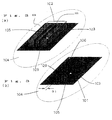
- the configuration of the antenna apparatus in embodiment 1 will be described with reference to FIGS. 1A and 1B.
- a dielectric 102 is inserted between a linear radiating element 101 that is rectilinear in shape and a patch type radiating element 103, whereas a dielectric 102 is not inserted in the antenna apparatus shown in FIG. 1B; the antenna apparatus of the present embodiment below has a configuration in which a dielectric is inserted.
- the linear radiating element 101 is made of metal, and has a feed terminal 105 that is given common termination via a sharing unit (not shown) and is connected to the reception input terminal (not shown) and transmission output terminal (not shown) of a communication apparatus (not shown).
- the linear radiating element 101 in embodiment 1 corresponds to the first radiating element of the present invention.
- the patch type radiating element 103 is made of metal, and is located opposite the linear radiating element 101.
- the patch type radiating element 103 in embodiment 1 corresponds to the second radiating element of the present invention.
- the earth plate 104 is made of metal, and is located on the opposite side to the linear radiating element 101 with respect to the patch type radiating element 103, and opposite the patch type radiating element 103.
- the earth plate 104 is earthed and has an essentially infinite area.
- the earth plate 104 in embodiment 1 corresponds to the earth of the present invention.
- the inductance 109 is a metal tab for connecting the linear radiating element 101 and the patch type radiating element 103, and stabilizing the potential of the linear radiating element 101.
- the dielectric 102 is a part formed from ceramic material that is inserted between the linear radiating element 101 and patch type radiating element 103, and has the function of a spacer.
- the dielectric 102 also supports the linear radiating element 101.
- the design parameter standards when the transmission band frequency is 1453 MHz to 1465 MHz and the reception band frequency is 1501 MHz to 1513 MHz are as follows.
- the limit of the height H1 of the linear radiating element 101 with respect to the patch type radiating element 103 is about 1/20 of the electric wave wavelength.
- the limit of the height H2 of the patch type radiating element 103 with respect to the earth plate 104 is about 1/60 of the electric wave wavelength.
- the limit of the length L1 of the linear radiating element 101 is about 1/4 of the electric wave wavelength.
- the limit of the circumferential length L2 of the patch type radiating element 103 is about 1/2 of the electric wave wavelength.
- FIG. 2 is a schematic drawing for explaining the transmission operation of the antenna apparatus in embodiment 1.
- the reception operation of the antenna apparatus in embodiment 1 is understood as virtually the opposite of the transmission operation described below, only the transmission operation will be described below.
- the transmission output terminal (not shown) of the communication apparatus performs signal output to the linear radiating element 101 via the feed terminal 105.
- an electric field 151 is generated between the linear radiating element 101 and the patch type radiating element 103. Also, due to the above described signal output from the communication apparatus (not shown), an electric field 152 is generated between the patch type radiating element 103 and the earth plate 104.
- the electric field 150 which is the composite sum of electric field 151 and electric field 152, is sent as the transmission electric wave.
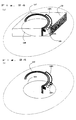
- the earth plate 104 in embodiment 1 need not have an essentially infinite area, and as shown in FIG. 6, need only have an area roughly 3 times or more the area of the patch type radiating element 103.
- FIG. 6 is an oblique drawing of an antenna apparatus that has an earth plate 201 with a finite area.
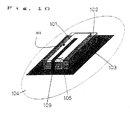
- FIG. 10 is an oblique drawing of an antenna apparatus with a printed circuit board 301 installed.
- the configuration of the antenna apparatus in embodiment 2 will be described with reference to FIGS. 3A and 3B.
- a dielectric 102 is inserted between a linear radiating element 101 and a patch type radiating element 103, whereas such a dielectric is not inserted in the antenna apparatus shown in FIG. 3B; the antenna apparatus of the present embodiment below has a configuration in which a dielectric is inserted.
- the antenna apparatus in embodiment 2 differs from the antenna apparatus in embodiment 1 in being equipped with a linear parasitic element 106 that is rectilinear in shape, described next.
- the linear parasitic element 106 is a part made of metal that does not have a feed terminal and is fitted parallel to the linear radiating element 101. As already explained, due to the presence of the linear parasitic element 106, the gain of the antenna apparatus in embodiment 2 is better than the gain of the antenna apparatus in embodiment 1.
- the limit of the gap D1 between the linear radiating element 101 and the linear parasitic element 106 is about 1/600 of the electric wave wavelength.
- the operation of the antenna apparatus in embodiment 2 that has this kind of configuration is the same as the operation of the antenna apparatus in embodiment 1.
- the earth plate 104 in embodiment 2 need not have an essentially infinite area, and as shown in FIG. 7, need only have an area roughly 3 times or more the area of the patch type radiating element 103.
- FIG. 7 is an oblique drawing of an antenna apparatus that has an earth plate 201 with a finite area.
- FIG. 11 is an oblique drawing of an antenna apparatus with a printed circuit board 301 installed.
- the configuration of the antenna apparatus in embodiment 3 will be described with reference to FIGS. 4A and 4B.
- a dielectric 102 is inserted between a spiral radiating element 107 and a circular patch type radiating element 108, whereas a dielectric 102 is not inserted in the antenna apparatus shown in FIG. 4B; the antenna apparatus of the present embodiment below has a configuration in which a dielectric is inserted.
- the spiral radiating element 107 is made of metal, and has a feed terminal 105 that is given common termination via a sharing unit (not shown) and is connected to the reception input terminal (not shown) and transmission output terminal (not shown) of a communication apparatus (not shown).
- the spiral radiating element 107 in embodiment 3 corresponds to the first radiating element of the present invention.
- the circular patch type radiating element 108 is made of metal, and is located opposite the spiral radiating element 107.
- the circular patch type radiating element 108 in embodiment 3 corresponds to the second radiating element of the present invention.
- the earth plate 104 is made of metal, and is located on the opposite side to the spiral radiating element 107 with respect to the circular patch type radiating element 108, and opposite the circular patch type radiating element 108.
- the earth plate 104 is earthed and has an essentially infinite area.
- the earth plate 104 in embodiment 3 corresponds to the earth of the present invention.
- the inductance 109 is a metal tab for connecting the spiral radiating element 107 and the circular patch type radiating element 108, and stabilizing the potential of the spiral radiating element 107.
- the dielectric 102 is a part formed from ceramic material that is inserted between the spiral radiating element 107 and circular patch type radiating element 108, and has the function of a spacer.
- the dielectric 102 also supports the spiral radiating element 107.
- the design parameter standards when the transmission band frequency is 1453 MHz to 1465 MHz and the reception band frequency is 1501 MHz to 1513 MHz are as follows.
- the limit of the height H3 of the spiral radiating element 107 with respect to the circular patch type radiating element 108 is about 1/20 of the electric wave wavelength.
- the limit of the height H4 of the circular patch type radiating element 108 with respect to the earth plate 104 is about 1/60 of the electric wave wavelength.
- the limit of the length L3 of the spiral radiating element 107 is about 1/4 of the electric wave wavelength.
- the limit of the circumferential length L4 of the circular patch type radiating element 108 is about 1/2 of the electric wave wavelength.
- the operation of the antenna apparatus in embodiment 3 that has this kind of configuration is the same as the operation of the antenna apparatus in embodiment 1.
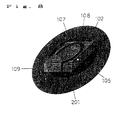
- the earth plate 104 in embodiment 3 need not have an essentially infinite area, and as shown in FIG. 8, need only have an area roughly 3 times or more the area of the circular patch type radiating element 108.
- FIG. 8 is an oblique drawing of an antenna apparatus that has an earth plate 201 with a finite area.
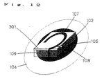
- FIG. 12 is an oblique drawing of an antenna apparatus with a printed circuit board 301 installed.
- the configuration of the antenna apparatus in embodiment 4 will be described with reference to FIGS. 5A and 5B.
- a dielectric 102 is inserted between a spiral radiating element 107 and a circular patch type radiating element 108, whereas such a dielectric is not inserted in the antenna apparatus shown in FIG. 5B; the antenna apparatus of the present embodiment below has a configuration in which a dielectric is inserted.
- the antenna apparatus in embodiment 4 differs from the antenna apparatus in embodiment 3 in being equipped with a spiral parasitic element 110, described next.
- the spiral parasitic element 110 is a part made of metal that does not have a feed terminal and is fitted parallel to the spiral radiating element 107. As already explained, due to the presence of the spiral parasitic element 110, the gain of the antenna apparatus in embodiment 4 is better than the gain of the antenna apparatus in embodiment 3.
- the limit of the gap D2 between the spiral radiating element 107 and the spiral parasitic element 110 is about 1/600 of the electric wave wavelength.
- the operation of the antenna apparatus in embodiment 4 that has this kind of configuration is the same as the operation of the antenna apparatus in embodiment 3.
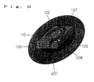
- the earth plate 104 in embodiment 4 need not have an essentially infinite area, and as shown in FIG. 9, need only have an area roughly 3 times or more the area of the circular patch type radiating element 108.
- FIG. 9 is an oblique drawing of an antenna apparatus that has an earth plate 201 with a finite area.
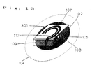
- FIG. 13 is an oblique drawing of an antenna apparatus with a printed circuit board 301 installed.
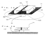
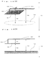
- FIG. 14A is an oblique drawing of the antenna apparatus in embodiment 5
- FIG. 14B is a front view of the antenna apparatus in embodiment 5.
- a linear radiating element supporting stand 501 is installed on a patch type radiating element 103, and supports a linear radiating element 101. To prevent the occurrence of disturbance of the electric field, the linear radiating element supporting stand 501 is installed outside the area of opposition 503 of the linear radiating element 101 and the patch type radiating element 103.
- a patch type radiating element supporting pillar 502 is installed on the earth plate 104, and supports the linear radiating element 101.
- the linear radiating element supporting stand 501 and the patch type radiating element supporting pillar 502 in embodiment 5 corresponds to the supports of the present invention.
- the operation of the antenna apparatus in embodiment 5 that has this kind of configuration is the same as the operation of the antenna apparatus in embodiment 1.
- FIG. 15A is an oblique drawing of an antenna apparatus with a linear parasitic element 106 mounted in parallel
- FIG. 15B is a front view of an antenna apparatus with a linear parasitic element 106 mounted in parallel.
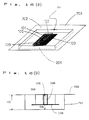
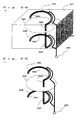
- FIG. 16A is an oblique drawing of the antenna apparatus in embodiment 6, and FIG. 16B is a cross-sectional drawing of the antenna apparatus in embodiment 6.
- the antenna apparatus in embodiment 6 differs from the antenna apparatus that has an earth plate 201 with a finite area in embodiment 1 in being equipped with a case 701, described next.
- the case 701 is integrated with the earth plate 201, and houses the linear radiating element 101 and patch type radiating element 103.
- the case 701 has an edge 703, the area above which 702 is open.
- the height H5 of the case 701, as also shown in FIG. 16B, is virtually equal to the height H6 of the linear radiating element 101 with respect to the earth plate 104.
- the operation of the antenna apparatus in embodiment 6 that has this kind of configuration is the same as the operation of the antenna apparatus in embodiment 1.
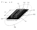
- FIG. 17 is an oblique drawing of the antenna apparatus in embodiment 7.
- the antenna apparatus in embodiment 7 differs from the antenna apparatus in embodiment 1 in being equipped with a cable earth 801, described next.
- the cable earth 801 is a metal tab, earthed by an earth 802, for stabilizing the potential of the patch type radiating element 103.
- the cable earth 801 embodiment 7 corresponds to the earth position determining tab of the present invention. It is sufficient for the length L5 from the cable earth 801 to the front end of the linear radiating element 101 to be about 1/4 of the electric wave wavelength. That is to say, as the cable earth 801 is fitted, it is sufficient simply to set the length from there to the front end of the linear radiating element 101 to about 1/4 of the electric wave wavelength, thus simplifying the manufacture of an antenna apparatus.
- the operation of the antenna apparatus in embodiment 7 that has this kind of configuration is the same as the operation of the antenna apparatus in embodiment 1.
- FIG. 18A is an oblique drawing of the antenna apparatus in embodiment 8
- FIG. 18B is a cross-sectional drawing of the antenna apparatus in embodiment 8.
- the antenna apparatus in embodiment 8 differs from the antenna apparatus in embodiment 5 in being equipped with a cover 901, described next.
- the cover 901 covers the linear radiating element 101, patch type radiating element 103, and earth plate 104, and is formed from ABS.
- the size D3 of the space between the cover 901 and the linear radiating element 101 should preferably be about 1/60 of the electric wave wavelength or more; tuning frequency drift is avoided by this means.
- the cover 901 also protects the linear radiating element 101, patch type radiating element 103, and earth plate 104.
- the operation of the antenna apparatus in embodiment 8 that has this kind of configuration is the same as the operation of the antenna apparatus in embodiment 5.
- FIG. 19A is an oblique drawing of the antenna apparatus in embodiment 9
- FIG. 19B is a front view of the antenna apparatus in embodiment 9.
- the antenna apparatus in embodiment 9 differs from the antenna apparatus in embodiment 1 in being equipped with a linear radiating element 1001 that extends beyond the patch type radiating element 103.
- the linear radiating element 1001 extends beyond the patch type radiating element 103 as shown in FIG. 19. For this reason, the electric field 154 described later can be used for electric wave transmission and reception.
- the linear radiating element 1001 in embodiment 9 corresponds to the first radiating element of the present invention.
- the transmission output terminal (not shown) of the communication apparatus performs signal output to the linear radiating element 1001 via the feed terminal 105.
- an electric field 151 is generated between the linear radiating element 1001 and the patch type radiating element 103, and an electric field 152 is generated between the patch type radiating element 103 and the earth plate 104. Also, an electric field 154 is generated between the linear radiating element 1001 and the earth plate 104. Thus, in embodiment 9, an electric field 154 is also generated between the linear radiating element 1001 and the earth plate 104.
- the electric field 153 which is the composite sum of electric field 151, electric field 152, and electric field 154, is sent as the transmission electric wave.
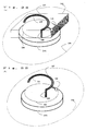
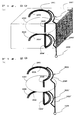
- the configuration of the antenna apparatus in embodiment 10 will be described with reference to FIGS. 22A and 22B.
- a dielectric 102 is inserted between a spiral radiating element 107 and a circular patch type radiating element 108, whereas such a dielectric is not inserted in the antenna apparatus shown in FIG. 22B; the antenna apparatus of the present embodiment below has a configuration in which a dielectric is inserted.
- the antenna apparatus in embodiment 10 differs from the antenna apparatus in embodiment 4 in being equipped with a metal pedestal 1101, described next.
- the metal pedestal 1101 is located between the circular patch type radiating element 108 and the earth plate 104, and is in contact with the earth plate 104 but is not in contact with the circular patch type radiating element 108.
- the metal pedestal 1101 contacts the earth plate 104 by means of a magnet, etc., and can easily be attached to and detached from the earth plate 104.
- the spiral radiating element 107, spiral parasitic element 110, circular patch type radiating element 108, and feed terminal 105 are integrated with the metal pedestal 1101, and together with the metal pedestal 1101 configure an antenna apparatus that can easily be moved from place to place. (Also, by inserting insulating material between the circular patch type radiating element 108 and the metal pedestal 1101, the circular patch type radiating element 108 can be kept essentially out of contact with the metal pedestal 1101.)
- the metal pedestal 1101 is an electric conductor. Therefore, through the contact between the metal pedestal 1101 and the earth plate 104, the metal pedestal 1101 functions effectively as an earth for the spiral radiating element 107 and circular patch type radiating element 108.
- the side of the dielectric 102 toward the spiral radiating element 107 is in contact with the spiral radiating element 107, and the side of the dielectric 102 toward the circular patch type radiating element 108 is in contact with the circular patch type radiating element 108.
- the operation of the antenna apparatus in embodiment 10 that has this kind of configuration is the same as the operation of the antenna apparatus in embodiment 4.
- the configuration of the antenna apparatus in embodiment 11 will be described with reference to FIGS. 23A and 23B.
- a dielectric 102 is inserted between a spiral radiating element 107 and a circular patch type radiating element 108, whereas such a dielectric is not inserted in the antenna apparatus shown in FIG. 23B; the antenna apparatus of the present embodiment below has a configuration in which a dielectric is inserted.
- the antenna apparatus in embodiment 11 differs from the antenna apparatus in embodiment 7 in being equipped with a feeder line 1201.
- the feeder line 1201 is a line for extending the feed terminal 105 up to the vicinity of the cable earth 801. Providing the feeder line 1201 enables the antenna apparatus to be easily connected to the communication apparatus (not shown).
- the cable ground of the coaxial cable is connected to the cable earth 801, and the coaxial cable signal line is connected to the feed terminal 105.
- the operation of the antenna apparatus in embodiment 11 that has this kind of configuration is the same as the operation of the antenna apparatus in embodiment 7.
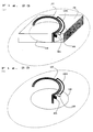
- the configuration of the antenna apparatus in embodiment 12 will be described with reference to FIGS. 24A and 24B.
- a dielectric 102 is inserted between a spiral radiating element 107 and a circular patch type radiating element 108, whereas such a dielectric is not inserted in the antenna apparatus shown in FIG. 24B; the antenna apparatus of the present embodiment below has a configuration in which a dielectric is inserted.
- the antenna apparatus in embodiment 12 differs from the antenna apparatus in embodiment 11 in being equipped with a capacitor 1301.
- the capacitor 1301 is connected between the feeder line 1201 and the coaxial cable signal line (as described in embodiment 11, the cable ground of the coaxial cable is connected to the cable earth, and the coaxial cable signal line is connected to the feed terminal). By connecting the capacitor, it is possible to cancel the reactance component generated by the feeder line and to measure only the actual impedance component, making it easy to achieve antenna impedance matching.
- the operation of the antenna apparatus in embodiment 12 that has this kind of configuration is the same as the operation of the antenna apparatus in embodiment 1.
- the configuration of the antenna apparatus in embodiment 13 will be described with reference to FIGS. 25A and 25B.
- a dielectric 102 is inserted between a spiral radiating element 107 and a circular patch type radiating element 108, whereas such a dielectric is not inserted in the antenna apparatus shown in FIG. 25B; the antenna apparatus of the present embodiment below has a configuration in which a dielectric is inserted.
- the antenna apparatus in embodiment 13 differs from the antenna apparatus in embodiment 11 with respect to equipped position of a cable earth 801 described next.
- the operation of the antenna apparatus in embodiment 13 that has this kind of configuration is the same as the operation of the antenna apparatus in embodiment 11.
- a dielectric 2007 is inserted between (1) a first spiral radiating element 2001 and a spiral parasitic element 2004 installed parallel to the first spiral radiating element 2001, and (2) a second spiral radiating element 2002 and a spiral parasitic element 2004' installed parallel to the second spiral radiating element 2002, whereas such a dielectric is not inserted in the antenna apparatus shown in FIG. 26B; the antenna apparatus of the present embodiment below has a configuration in which a dielectric is inserted.
- the first spiral radiating element 2001 and second spiral radiating element 2002 are both made of metal, and have a feed terminal 2005 that is given common termination via a sharing unit (not shown) and is connected to the reception input terminal (not shown) and transmission output terminal (not shown) of a communication apparatus (not shown).
- the second spiral radiating element 2002 is located on the opposite side to the first spiral radiating element 2001 with respect to a circular patch type element 2003 made of metal, and is located opposite the circular patch type element 2003.
- the first spiral radiating element 2001 corresponds to the first radiating element of the present invention
- the second spiral radiating element 2002 corresponds to the third radiating element of the present invention
- the circular patch type element 2003 corresponds to the second radiating element of the present invention.
- an inductance 2006 connects the first spiral radiating element 2001 and the circular patch type element 2003, and an inductance 2006' connects the second spiral radiating element 2002 and the circular patch type element 2003.
- metal tabs for stabilizing the potential of the first spiral radiating element 2001 and second spiral radiating element 2002.
- the dielectric 2007 is a part formed from ceramic material that is inserted between (1) the first spiral radiating element 2001 and the spiral parasitic element 2004 installed parallel to the first spiral radiating element 2001, and (2) the second spiral radiating element 2002 and the spiral parasitic element 2004' installed parallel to the second spiral radiating element 2002, and has the function of a spacer.
- the dielectric 2007 also supports the first spiral radiating element 2001 and second spiral radiating element 2002.
- a first feeder line 2022 is connected to the first spiral radiating element 2001, and a second feeder line 2022' is connected to the second spiral radiating element 2002; common feeding to these is performed from the feed terminal 2005.
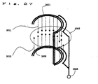
- FIG. 27 is a type drawing for explaining the transmission operation of the antenna apparatus in embodiment 14.
- the reception operation of the antenna apparatus in embodiment 14 is understood as virtually the opposite of the transmission operation described below, only the transmission operation will be described below.
- the communication apparatus (not shown) performs the same kind of signal output as in embodiment 1 to the first spiral radiating element 2001 and the second spiral radiating element 2002 via the feed terminal 2005.
- an electric field 2011 is generated between the first spiral radiating element 2001 and the circular patch type element 2003.
- an electric field 2012 is generated between the second spiral radiating element 2002 and the circular patch type element 2003.
- there is no earth opposite the circular patch type element 2003 there is no electric field radiated from the circular patch type element 2003.
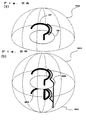
- FIG. 28A is a schematic drawing for explaining the directivity of the antenna apparatus in embodiments 1 to 13
- FIG. 28B is a schematic drawing for explaining the directivity of the antenna apparatus in embodiments 14 to 16.
- a dielectric 2007 is inserted between (1) a first spiral radiating element 2001 and a spiral parasitic element 2004 installed parallel to the first spiral radiating element 2001, and (2) a second spiral radiating element 2002 and a spiral parasitic element 2004' installed parallel to the second spiral radiating element 2002, whereas such a dielectric is not inserted in the antenna apparatus shown in FIG. 29B; the antenna apparatus of the present embodiment below has a configuration in which a dielectric is inserted.
- the antenna apparatus in embodiment 16 differs from the antenna apparatus in embodiment 14 in being equipped with capacitors 2021 and 2021', described next.
- Capacitor 2021 is connected to the first feeder line 2022 on the first spiral radiating element 2001 side, and capacitor 2021' is connected to the second feeder line 2022' on the second spiral radiating element 2002 side. By connecting the capacitors, it is possible to cancel the reactance component generated by the feeder line and to measure only the actual impedance component, making it easy to achieve antenna impedance matching.
- the operation of the antenna apparatus in embodiment 16 that has this kind of configuration is the same as the operation of the antenna apparatus in embodiment 14.
- a dielectric 2007 is inserted between (1) a first spiral radiating element 2001 and a spiral parasitic element 2004 installed parallel to the first spiral radiating element 2001, and (2) a second spiral radiating element 2002 and a spiral parasitic element 2004' installed parallel to the second spiral radiating element 2002, whereas such a dielectric is not inserted in the antenna apparatus shown in FIG. 30B; the antenna apparatus of the present embodiment below has a configuration in which a dielectric is inserted.
- the antenna apparatus in embodiment 16 differs from the antenna apparatus in embodiment 14 in being equipped with a mixer 2031, described next.
- the mixer 2031 is connected between a first feeder line 2032 on the first spiral radiating element 2001 side and a second feeder line 2033 on the second spiral radiating element 2002 side, and is means for performing feeding from the feed terminal 2005 via the mixer 2031.
- the mixer 2031 the signal on the first spiral radiating element 2001 side and the signal on the second spiral radiating element 2002 side are separated, and the degree of separation of the first spiral radiating element 2001 and the second spiral radiating element 2002 is improved. By this means, it is possible to eliminate mutual influence between the first spiral radiating element 2001 and the second spiral radiating element 2002.
- the operation of the antenna apparatus in embodiment 16 that has this kind of configuration is the same as the operation of the antenna apparatus in embodiment 14.
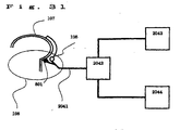
- a coaxial cable 2041 is connected to the antenna apparatus in embodiment 13.
- the coaxial cable 2041 connects the antenna apparatus to a communication apparatus for linear polarization 2043 and a communication apparatus for circular polarization 2044 via a distributor 2042;
- the antenna apparatus shown in FIG. 31 is the antenna apparatus in embodiment 13 (but with the dielectric not shown), and as described above, the cable ground of the coaxial cable is connected to the cable earth 801, and the coaxial cable signal line is connected to the feed terminal 105.
- the antenna apparatus connected to the coaxial cable 2041 may be the antenna apparatus in any of the above described embodiments, and, as described above, is an antenna apparatus with hemispherical directivity in embodiments 1 to 13, or with spherical directivity in embodiments 14 to 16.
- the antenna apparatus in embodiment 13 that has hemispherical directivity is provided with transmission and reception capability for both the linear polarization used in ground communication and the circular polarization used in communication with an artificial satellite, and an antenna apparatus that has spherical directivity (such as the antenna apparatus in embodiment 14) is also provided with transmission and reception capability for both linear polarization and circular polarization).
- both a communication apparatus that receives electric waves from the ground and a communication apparatus that receives electric waves from an artificial satellite can be used simultaneously with a single antenna apparatus, enabling the configuration of a communication system to be simplified.
- the feed terminal in the present invention need not be provided on the first radiating element as in embodiments 1 to 13, but may instead be provided on the second radiating element.
- the inductance in the present invention is provided in the above described embodiments, but this is not a limitation, and it need not be provided. However, in a case where, for example, the inductance 109 is not provided, the limit of the length L1 of the linear radiating element 101, and the limit of the length L3 of the spiral radiating element 107, are both about 1/2 of the electric wave wavelength.
- the dielectric in the present invention need not be formed from ceramic material as in the above described embodiments, but may instead be formed from Dupont, Teflon, epoxy resin, ABS, etc. Further, the dielectric in the present invention is inserted, in the above described embodiments, only between the first radiating element and second radiating element of the present invention, but this is not a limitation, and, for example, it may instead (1) be inserted so that the first radiating element and second radiating element are contained therein, or (2) be inserted so that the first radiating element and third radiating element are contained therein, or (3) be inserted between the first radiating element and second radiating element and/or between the second radiating element and third radiating element, or (4) not be inserted.
- a lower antenna apparatus height is realized by inserting a dielectric with a high dielectric constant.
- cover in the present invention need not be formed from ceramic material as in the above described embodiments, but may instead be formed from Dupont, Teflon, epoxy resin, ABS, etc.
- first radiating element and third radiating element in the present invention are both spiral in shape in above described embodiments 14 to 16, but this is not a limitation, and instead, for example, (1) both may be linear in shape, or (2) the first radiating element may be linear in shape while the third radiating element is spiral in shape.
- first radiating element and third radiating element in the present invention are each provided with a parallel spiral parasitic element in above described embodiments 14 to 16, but this is not a limitation, and instead, for example, (1) neither may be provided with a parallel spiral parasitic element, or (2) only the first radiating element may be provided with a parallel spiral parasitic element.
- a first feeder line is provided for the first radiating element in the present invention
- a second feeder line is provided for the second radiating element in the present invention
- common feeding is performed for the first feeder line and the second feeder line, but this is not a limitation, and instead, for example, it is possible (1) for the first feeder line and/or second feeder line not to be provided, and feeding to be performed directly, or (2) for feeding to be performed independently to the first feeder line and the second feeder line regardless of whether or not feeder lines are provided.
- the pedestal in the present invention is an electric conductor in above described embodiment 10, but this is not a limitation, and it need not be an electric conductor.
- the reactance element in the present invention is a capacitor in the above described embodiments, but this is not a limitation, and it may instead be a coil, etc.
- a first present invention corresponding to claim 1 can provide an antenna apparatus characterized by realizing high gain and an increase in specific bandwidth.
- a second present invention corresponding to claim 2 can provide an antenna apparatus characterized by having stable operation, in addition to the above described effects.
- a third present invention corresponding to claim 3 can provide an antenna apparatus characterized by having a simple structure, in addition to the above described effects.
- a fourth present invention corresponding to claim 4 can provide an antenna apparatus characterized by realizing high gain, in addition to the above described effects.
- a fifth present invention corresponding to claim 5 can provide an antenna apparatus characterized by having a simple structure, in addition to the above described effects.
- a sixth present invention corresponding to claim 6 can provide an antenna apparatus characterized by realizing high gain, in addition to the above described effects.
- a seventh present invention corresponding to claim 7 can provide an antenna apparatus characterized by realizing a low apparatus height, in addition to the above described effects.
- An eighth present invention corresponding to claim 8 can provide an antenna apparatus characterized by realizing a small apparatus size, in addition to the above described effects.
- a ninth present invention corresponding to claim 9 can provide an antenna apparatus characterized by realizing compactness of the apparatus, in addition to the above described effects.
- a tenth present invention corresponding to claim 10 can provide an antenna apparatus characterized by having a stable structure, in addition to the above described effects.
- An eleventh present invention corresponding to claim 11 can provide an antenna apparatus characterized by not requiring a separate case, in addition to the above described effects.
- a twelfth present invention corresponding to claim 12 can provide an antenna apparatus characterized by the fact that manufacture is simple, in addition to the above described effects.
- a thirteenth present invention corresponding to claim 13 can provide an antenna apparatus characterized by little noise and by having good durability, in addition to the above described effects.
- a fourteenth present invention corresponding to claim 14 can provide an antenna apparatus characterized by improving simplicity of setting the apparatus, in addition to the above described effects.
- a fifteenth present invention corresponding to claim 15 can provide an antenna apparatus characterized by having stable operation, in addition to the above described effects.
- a sixteenth present invention corresponding to claim 16 can provide an antenna apparatus characterized by greater simplicity of performance adjustment in manufacture, in addition to the above described effects.
- a seventeenth present invention corresponding to claim 17 can provide an antenna apparatus characterized by realizing high gain, in addition to the above described effects.
- An eighteenth present invention corresponding to claim 18 can provide an antenna apparatus characterized by having high gain in all directions three-dimensionally, in addition to the above described effects.
- a nineteenth present invention corresponding to claim 19 can provide an antenna apparatus characterized by a small difference in gain according to direction, and stable high gain in all directions, in addition to the above described effects.
- a twentieth present invention corresponding to claim 20 can provide an antenna apparatus characterized by realizing high gain, in addition to the above described effects.
- a twenty-first present invention corresponding to claim 21 can provide an antenna apparatus characterized by realizing a low apparatus height, in addition to the above described effects.
- a twenty-second present invention corresponding to claim 22 can provide an antenna apparatus characterized by having a simple structure, in addition to the above described effects.
- a twenty-third present invention corresponding to claim 23 can provide an antenna apparatus characterized by greater simplicity of performance adjustment in manufacture, in addition to the above described effects.
- a twenty-fourth present invention corresponding to claim 24 can provide an antenna apparatus characterized by having stable operation, in addition to the above described effects.
- a twenty-fifth present invention corresponding to claim 25 can provide a communication system characterized by having a simple structure.
- a twenty-sixth present invention corresponding to claim 26 can provide a communication system characterized by having a simple structure.
Landscapes
- Physics & Mathematics (AREA)
- Electromagnetism (AREA)
- Waveguide Aerials (AREA)
- Variable-Direction Aerials And Aerial Arrays (AREA)
- Details Of Aerials (AREA)
- Support Of Aerials (AREA)
Priority Applications (1)
| Application Number | Priority Date | Filing Date | Title |
|---|---|---|---|
| EP05024605A EP1626458A3 (de) | 1999-10-08 | 2000-10-05 | Antennenanordnung und Kommunikationssystem |
Applications Claiming Priority (4)
| Application Number | Priority Date | Filing Date | Title |
|---|---|---|---|
| JP28855099 | 1999-10-08 | ||
| JP28855099 | 1999-10-08 | ||
| JP2000127611 | 2000-04-27 | ||
| JP2000127611A JP2001177326A (ja) | 1999-10-08 | 2000-04-27 | アンテナ装置、通信システム |
Related Child Applications (1)
| Application Number | Title | Priority Date | Filing Date |
|---|---|---|---|
| EP05024605A Division EP1626458A3 (de) | 1999-10-08 | 2000-10-05 | Antennenanordnung und Kommunikationssystem |
Publications (3)
| Publication Number | Publication Date |
|---|---|
| EP1091445A2 true EP1091445A2 (de) | 2001-04-11 |
| EP1091445A3 EP1091445A3 (de) | 2003-03-26 |
| EP1091445B1 EP1091445B1 (de) | 2006-02-22 |
Family
ID=26557229
Family Applications (2)
| Application Number | Title | Priority Date | Filing Date |
|---|---|---|---|
| EP05024605A Withdrawn EP1626458A3 (de) | 1999-10-08 | 2000-10-05 | Antennenanordnung und Kommunikationssystem |
| EP00121779A Expired - Lifetime EP1091445B1 (de) | 1999-10-08 | 2000-10-05 | Antennenanordnung und Kommunikationssystem |
Family Applications Before (1)
| Application Number | Title | Priority Date | Filing Date |
|---|---|---|---|
| EP05024605A Withdrawn EP1626458A3 (de) | 1999-10-08 | 2000-10-05 | Antennenanordnung und Kommunikationssystem |
Country Status (5)
| Country | Link |
|---|---|
| US (1) | US6608594B1 (de) |
| EP (2) | EP1626458A3 (de) |
| JP (1) | JP2001177326A (de) |
| CN (1) | CN1212691C (de) |
| DE (1) | DE60026098T2 (de) |
Cited By (4)
| Publication number | Priority date | Publication date | Assignee | Title |
|---|---|---|---|---|
| WO2005076407A3 (en) * | 2004-01-30 | 2005-10-06 | Fractus Sa | Multi-band monopole antennas for mobile communications devices |
| US7403164B2 (en) | 2002-12-22 | 2008-07-22 | Fractus, S.A. | Multi-band monopole antenna for a mobile communications device |
| US7423593B2 (en) | 2003-01-24 | 2008-09-09 | Carles Puente Baliarda | Broadside high-directivity microstrip patch antennas |
| EP2575212A1 (de) * | 2011-09-28 | 2013-04-03 | LG Innotek Co., Ltd. | Antenne |
Families Citing this family (12)
| Publication number | Priority date | Publication date | Assignee | Title |
|---|---|---|---|---|
| JP2002237711A (ja) * | 2000-12-08 | 2002-08-23 | Matsushita Electric Ind Co Ltd | アンテナ装置、および通信システム |
| CN2476881Y (zh) * | 2000-12-30 | 2002-02-13 | 深圳市中兴通讯股份有限公司 | 一种手机内置式平面天线 |
| TW527754B (en) * | 2001-12-27 | 2003-04-11 | Ind Tech Res Inst | Dual-band planar antenna |
| JP2004201278A (ja) * | 2002-12-06 | 2004-07-15 | Sharp Corp | パターンアンテナ |
| US7119743B2 (en) | 2003-06-09 | 2006-10-10 | Matsushita Electric Industrial Co., Ltd. | Antenna and electronic device using the same |
| US7333057B2 (en) | 2004-07-31 | 2008-02-19 | Harris Corporation | Stacked patch antenna with distributed reactive network proximity feed |
| US7656353B2 (en) * | 2005-11-29 | 2010-02-02 | Research In Motion Limited | Mobile wireless communications device comprising a satellite positioning system antenna with active and passive elements and related methods |
| US9160074B2 (en) * | 2008-03-05 | 2015-10-13 | Ethertronics, Inc. | Modal antenna with correlation management for diversity applications |
| GB0806335D0 (en) * | 2008-04-08 | 2008-05-14 | Antenova Ltd | A novel planar radio-antenna module |
| US10431873B2 (en) | 2016-06-20 | 2019-10-01 | Shure Acquisitions Holdings, Inc. | Diversity antenna for bodypack transmitter |
| KR102471197B1 (ko) * | 2016-08-25 | 2022-11-28 | 삼성전자 주식회사 | 안테나 장치 및 이를 포함하는 전자 장치 |
| EP3761447B1 (de) * | 2018-04-25 | 2022-08-31 | Huawei Technologies Co., Ltd. | Antenne und mobiles endgerät |
Family Cites Families (59)
| Publication number | Priority date | Publication date | Assignee | Title |
|---|---|---|---|---|
| US2520988A (en) | 1948-03-31 | 1950-09-05 | Motorola Inc | Car body antenna |
| FR1219279A (fr) * | 1958-12-20 | 1960-05-17 | Sagem | Antenne perfectionnée à très large bande |
| US3624658A (en) * | 1970-07-09 | 1971-11-30 | Textron Inc | Broadband spiral antenna with provision for mode suppression |
| SE388102B (sv) | 1973-11-30 | 1976-09-20 | Ericsson Telefon Ab L M | Anleggning for automatisk overforing av information fran en informationsgivare till en informationssokare |
| JPS56713A (en) | 1979-06-14 | 1981-01-07 | Matsushita Electric Ind Co Ltd | Antenna unit |
| JPS5631235A (en) | 1979-08-23 | 1981-03-30 | Pioneer Electronic Corp | Active antenna system |
| JPS6278379A (ja) | 1985-09-30 | 1987-04-10 | 日産自動車株式会社 | 車両用施解錠制御装置 |
| CA1263745A (en) * | 1985-12-03 | 1989-12-05 | Nippon Telegraph & Telephone Corporation | Shorted microstrip antenna |
| JPS6438845A (en) | 1987-04-21 | 1989-02-09 | Nec Corp | Processor normalcy confirming system |
| JPH01158808A (ja) | 1987-12-15 | 1989-06-21 | Sony Corp | 平面アレイアンテナ |
| US4958167A (en) | 1987-09-16 | 1990-09-18 | Schroeder Klaus G | Ultra-broadband impedance matched electrically small complementary signal radiating structures using thin wire elements and an impedance optimizing feed circuit |
| US4801944A (en) | 1987-10-13 | 1989-01-31 | Madnick Peter A | Antenna |
| US4823143A (en) | 1988-04-22 | 1989-04-18 | Hughes Aircraft Company | Intersecting shared aperture antenna reflectors |
| JPH0286201A (ja) | 1988-09-21 | 1990-03-27 | Harada Ind Co Ltd | 自動車用ループアンテナ |
| US5231407A (en) | 1989-04-18 | 1993-07-27 | Novatel Communications, Ltd. | Duplexing antenna for portable radio transceiver |
| JPH03263903A (ja) * | 1989-04-28 | 1991-11-25 | Misao Haishi | 小形アンテナ |
| JPH0353014A (ja) | 1989-07-17 | 1991-03-07 | Nippon Steel Corp | 極低硫鋼の溶製方法 |
| DE4003385C2 (de) | 1990-02-05 | 1996-03-28 | Hirschmann Richard Gmbh Co | Antennenanordnung |
| US5177493A (en) | 1990-03-05 | 1993-01-05 | Pioneer Electronic Corporation | Antenna device for movable body |
| US5043738A (en) * | 1990-03-15 | 1991-08-27 | Hughes Aircraft Company | Plural frequency patch antenna assembly |
| JPH04207303A (ja) | 1990-11-30 | 1992-07-29 | Hitachi Ltd | 車載用通信アンテナ |
| JPH04282903A (ja) | 1991-03-11 | 1992-10-08 | Mitsubishi Electric Corp | アレーアンテナ装置 |
| US5153600A (en) * | 1991-07-01 | 1992-10-06 | Ball Corporation | Multiple-frequency stacked microstrip antenna |
| JP2762782B2 (ja) | 1991-08-02 | 1998-06-04 | 松下電器産業株式会社 | 密閉電池 |
| JP2705392B2 (ja) * | 1991-09-04 | 1998-01-28 | 日本電気株式会社 | 携帯無線機 |
| JPH0570013A (ja) | 1991-09-13 | 1993-03-23 | Kato Hatsujo Kaisha Ltd | 高摩擦ローラ及びその製造法 |
| JPH082007B2 (ja) | 1991-12-24 | 1996-01-10 | 株式会社エイ・ティ・アール光電波通信研究所 | 2周波共用平面アンテナ |
| US5272485A (en) | 1992-02-04 | 1993-12-21 | Trimble Navigation Limited | Microstrip antenna with integral low-noise amplifier for use in global positioning system (GPS) receivers |
| FR2691015B1 (fr) * | 1992-05-05 | 1994-10-07 | Aerospatiale | Antenne-réseau de type micro-ruban à faible épaisseur mais à large bande passante. |
| US5572226A (en) | 1992-05-15 | 1996-11-05 | Micron Technology, Inc. | Spherical antenna pattern(s) from antenna(s) arranged in a two-dimensional plane for use in RFID tags and labels |
| JPH0669771A (ja) | 1992-08-20 | 1994-03-11 | Mitsubishi Electric Corp | 送受信モジュール |
| DE69331989T2 (de) * | 1992-12-07 | 2003-01-16 | Ntt Mobile Communications Network Inc., Tokio/Tokyo | Antennenvorrichtung |
| JPH0664105B2 (ja) | 1992-12-18 | 1994-08-22 | 株式会社巴川製紙所 | トナーの電荷量測定方法 |
| ES2159540T3 (es) | 1993-02-08 | 2001-10-16 | Koninkl Philips Electronics Nv | Receptor, con multiplexor de division ortogonal de frecuencia, con compensacion para retardos diferenciales. |
| US5420596A (en) | 1993-11-26 | 1995-05-30 | Motorola, Inc. | Quarter-wave gap-coupled tunable strip antenna |
| JP3326935B2 (ja) | 1993-12-27 | 2002-09-24 | 株式会社日立製作所 | 携帯無線機用小型アンテナ |
| JPH07336130A (ja) | 1994-06-08 | 1995-12-22 | Toyota Central Res & Dev Lab Inc | 移動体用アンテナ装置 |
| JPH0878943A (ja) | 1994-09-03 | 1996-03-22 | Nippon Dengiyou Kosaku Kk | 広帯域線状アンテナ |
| JP3539522B2 (ja) | 1994-12-20 | 2004-07-07 | 松下電器産業株式会社 | 直交周波数分割多重信号の伝送方法ならびにその送信装置および受信装置 |
| FR2732178A1 (fr) | 1995-03-22 | 1996-09-27 | Philips Electronique Lab | Systeme de transmission numerique muni d'un recepteur a egaliseurs cascades |
| US5627550A (en) | 1995-06-15 | 1997-05-06 | Nokia Mobile Phones Ltd. | Wideband double C-patch antenna including gap-coupled parasitic elements |
| JP2803614B2 (ja) | 1995-12-22 | 1998-09-24 | 日本電気株式会社 | 移動中継装置 |
| US5874926A (en) | 1996-03-11 | 1999-02-23 | Murata Mfg Co. Ltd | Matching circuit and antenna apparatus |
| US5680144A (en) * | 1996-03-13 | 1997-10-21 | Nokia Mobile Phones Limited | Wideband, stacked double C-patch antenna having gap-coupled parasitic elements |
| JPH09260925A (ja) | 1996-03-19 | 1997-10-03 | Matsushita Electric Ind Co Ltd | アンテナ装置 |
| JP3521613B2 (ja) * | 1996-05-14 | 2004-04-19 | カシオ計算機株式会社 | アンテナを備えた電子機器 |
| JP3296189B2 (ja) | 1996-06-03 | 2002-06-24 | 三菱電機株式会社 | アンテナ装置 |
| JP3126313B2 (ja) * | 1996-09-19 | 2001-01-22 | 松下電器産業株式会社 | アンテナ装置 |
| JP2971817B2 (ja) | 1996-10-01 | 1999-11-08 | 株式会社次世代デジタルテレビジョン放送システム研究所 | Ofdmダイバーシティ受信機の信号合成方式 |
| JP3580654B2 (ja) * | 1996-12-04 | 2004-10-27 | 京セラ株式会社 | 共用アンテナおよびこれを用いた携帯無線機 |
| US5874919A (en) * | 1997-01-09 | 1999-02-23 | Harris Corporation | Stub-tuned, proximity-fed, stacked patch antenna |
| EP0884796A3 (de) | 1997-06-11 | 1999-03-24 | Matsushita Electric Industrial Co., Ltd. | Antenne aus gebogenen oder gekrümmten Teilen eines linearen Leiters |
| US5929825A (en) * | 1998-03-09 | 1999-07-27 | Motorola, Inc. | Folded spiral antenna for a portable radio transceiver and method of forming same |
| US6166694A (en) * | 1998-07-09 | 2000-12-26 | Telefonaktiebolaget Lm Ericsson (Publ) | Printed twin spiral dual band antenna |
| US6353443B1 (en) | 1998-07-09 | 2002-03-05 | Telefonaktiebolaget Lm Ericsson (Publ) | Miniature printed spiral antenna for mobile terminals |
| US6343208B1 (en) | 1998-12-16 | 2002-01-29 | Telefonaktiebolaget Lm Ericsson (Publ) | Printed multi-band patch antenna |
| US6118406A (en) * | 1998-12-21 | 2000-09-12 | The United States Of America As Represented By The Secretary Of The Navy | Broadband direct fed phased array antenna comprising stacked patches |
| JP2001119238A (ja) | 1999-10-18 | 2001-04-27 | Sony Corp | アンテナ装置及び携帯無線機 |
| WO2001047063A1 (en) | 1999-12-22 | 2001-06-28 | Rangestar Wireless, Inc. | Low profile tunable circularly polarized antenna |
-
2000
- 2000-04-27 JP JP2000127611A patent/JP2001177326A/ja not_active Withdrawn
- 2000-10-05 DE DE60026098T patent/DE60026098T2/de not_active Expired - Fee Related
- 2000-10-05 US US09/680,263 patent/US6608594B1/en not_active Expired - Fee Related
- 2000-10-05 EP EP05024605A patent/EP1626458A3/de not_active Withdrawn
- 2000-10-05 EP EP00121779A patent/EP1091445B1/de not_active Expired - Lifetime
- 2000-10-06 CN CNB001306499A patent/CN1212691C/zh not_active Expired - Fee Related
Cited By (9)
| Publication number | Priority date | Publication date | Assignee | Title |
|---|---|---|---|---|
| US7403164B2 (en) | 2002-12-22 | 2008-07-22 | Fractus, S.A. | Multi-band monopole antenna for a mobile communications device |
| US7411556B2 (en) | 2002-12-22 | 2008-08-12 | Fractus, S.A. | Multi-band monopole antenna for a mobile communications device |
| US7675470B2 (en) | 2002-12-22 | 2010-03-09 | Fractus, S.A. | Multi-band monopole antenna for a mobile communications device |
| US7423593B2 (en) | 2003-01-24 | 2008-09-09 | Carles Puente Baliarda | Broadside high-directivity microstrip patch antennas |
| US8026853B2 (en) | 2003-01-24 | 2011-09-27 | Fractus, S.A. | Broadside high-directivity microstrip patch antennas |
| WO2005076407A3 (en) * | 2004-01-30 | 2005-10-06 | Fractus Sa | Multi-band monopole antennas for mobile communications devices |
| US7423592B2 (en) | 2004-01-30 | 2008-09-09 | Fractus, S.A. | Multi-band monopole antennas for mobile communications devices |
| EP2575212A1 (de) * | 2011-09-28 | 2013-04-03 | LG Innotek Co., Ltd. | Antenne |
| US9373890B2 (en) | 2011-09-28 | 2016-06-21 | Lg Innotek Co., Ltd. | Antenna |
Also Published As
| Publication number | Publication date |
|---|---|
| JP2001177326A (ja) | 2001-06-29 |
| DE60026098T2 (de) | 2006-08-10 |
| DE60026098D1 (de) | 2006-04-27 |
| HK1036158A1 (en) | 2001-12-21 |
| US6608594B1 (en) | 2003-08-19 |
| EP1091445B1 (de) | 2006-02-22 |
| EP1626458A2 (de) | 2006-02-15 |
| EP1091445A3 (de) | 2003-03-26 |
| EP1626458A3 (de) | 2006-03-01 |
| CN1212691C (zh) | 2005-07-27 |
| CN1292584A (zh) | 2001-04-25 |
Similar Documents
| Publication | Publication Date | Title |
|---|---|---|
| US6608594B1 (en) | Antenna apparatus and communication system | |
| EP0070150B1 (de) | Antennenanordnung für Sprechfunkgeräte | |
| KR100588765B1 (ko) | 원형 편파 유전체 공진기 안테나 | |
| US7696941B2 (en) | Printed circuit notch antenna | |
| US5668561A (en) | Antenna coupler | |
| US6239753B1 (en) | Transmitter-and-receiver device | |
| US6853341B1 (en) | Antenna means | |
| US6563468B2 (en) | Omni directional antenna with multiple polarizations | |
| US6384793B2 (en) | Slot antenna device | |
| US20090079637A1 (en) | Antenna apparatus for radio communication | |
| EP1355375A1 (de) | Doppelantenne | |
| KR20010102016A (ko) | 안테나 장치 및 안테나 장치를 포함하는 무선통신장치 | |
| JPH11239020A (ja) | 円偏波アンテナおよびそれを用いた無線装置 | |
| US6215456B1 (en) | Antenna unit and radio receiver device | |
| US7372412B2 (en) | Transceiver-integrated antenna | |
| KR20020033582A (ko) | 안테나 및 이것을 이용한 전파송수신장치, 및 안테나의제조방법 | |
| GB2272575A (en) | Dual band antenna | |
| US6229495B1 (en) | Dual-point-feed broadband whip antenna | |
| WO2002027862A1 (en) | Omni directional antenna with multiple polarizations | |
| US5668563A (en) | Integral type flat antenna provided with converter function | |
| JP3430809B2 (ja) | 送受信装置 | |
| CN115298902A (zh) | 天线模块 | |
| EP4716012A1 (de) | Antennenanordnung, kommunikationsvorrichtung und fahrzeug | |
| KR100861865B1 (ko) | 무선 단말기 | |
| KR102529334B1 (ko) | Mimo 안테나 및 이를 포함하는 mimo 안테나 장치 |
Legal Events
| Date | Code | Title | Description |
|---|---|---|---|
| PUAI | Public reference made under article 153(3) epc to a published international application that has entered the european phase |
Free format text: ORIGINAL CODE: 0009012 |
|
| AK | Designated contracting states |
Kind code of ref document: A2 Designated state(s): AT BE CH CY DE DK ES FI FR GB GR IE IT LI LU MC NL PT SE |
|
| AX | Request for extension of the european patent |
Free format text: AL;LT;LV;MK;RO;SI |
|
| PUAL | Search report despatched |
Free format text: ORIGINAL CODE: 0009013 |
|
| AK | Designated contracting states |
Kind code of ref document: A3 Designated state(s): AT BE CH CY DE DK ES FI FR GB GR IE IT LI LU MC NL PT SE |
|
| AX | Request for extension of the european patent |
Extension state: AL LT LV MK RO SI |
|
| 17P | Request for examination filed |
Effective date: 20030822 |
|
| 17Q | First examination report despatched |
Effective date: 20031001 |
|
| AKX | Designation fees paid |
Designated state(s): DE FR GB |
|
| GRAP | Despatch of communication of intention to grant a patent |
Free format text: ORIGINAL CODE: EPIDOSNIGR1 |
|
| GRAS | Grant fee paid |
Free format text: ORIGINAL CODE: EPIDOSNIGR3 |
|
| GRAA | (expected) grant |
Free format text: ORIGINAL CODE: 0009210 |
|
| AK | Designated contracting states |
Kind code of ref document: B1 Designated state(s): DE FR GB |
|
| REG | Reference to a national code |
Ref country code: GB Ref legal event code: FG4D |
|
| REF | Corresponds to: |
Ref document number: 60026098 Country of ref document: DE Date of ref document: 20060427 Kind code of ref document: P |
|
| ET | Fr: translation filed | ||
| PGFP | Annual fee paid to national office [announced via postgrant information from national office to epo] |
Ref country code: DE Payment date: 20060928 Year of fee payment: 7 |
|
| PGFP | Annual fee paid to national office [announced via postgrant information from national office to epo] |
Ref country code: GB Payment date: 20061004 Year of fee payment: 7 |
|
| PLBE | No opposition filed within time limit |
Free format text: ORIGINAL CODE: 0009261 |
|
| STAA | Information on the status of an ep patent application or granted ep patent |
Free format text: STATUS: NO OPPOSITION FILED WITHIN TIME LIMIT |
|
| 26N | No opposition filed |
Effective date: 20061123 |
|
| GBPC | Gb: european patent ceased through non-payment of renewal fee |
Effective date: 20071005 |
|
| PG25 | Lapsed in a contracting state [announced via postgrant information from national office to epo] |
Ref country code: DE Free format text: LAPSE BECAUSE OF NON-PAYMENT OF DUE FEES Effective date: 20080501 |
|
| REG | Reference to a national code |
Ref country code: FR Ref legal event code: ST Effective date: 20080630 |
|
| PGFP | Annual fee paid to national office [announced via postgrant information from national office to epo] |
Ref country code: FR Payment date: 20061010 Year of fee payment: 7 |
|
| PG25 | Lapsed in a contracting state [announced via postgrant information from national office to epo] |
Ref country code: GB Free format text: LAPSE BECAUSE OF NON-PAYMENT OF DUE FEES Effective date: 20071005 |
|
| PG25 | Lapsed in a contracting state [announced via postgrant information from national office to epo] |
Ref country code: FR Free format text: LAPSE BECAUSE OF NON-PAYMENT OF DUE FEES Effective date: 20071031 |