EP1091518A2 - Système et procédé pour la mesure d'erreurs de bits - Google Patents
Système et procédé pour la mesure d'erreurs de bits Download PDFInfo
- Publication number
- EP1091518A2 EP1091518A2 EP00121289A EP00121289A EP1091518A2 EP 1091518 A2 EP1091518 A2 EP 1091518A2 EP 00121289 A EP00121289 A EP 00121289A EP 00121289 A EP00121289 A EP 00121289A EP 1091518 A2 EP1091518 A2 EP 1091518A2
- Authority
- EP
- European Patent Office
- Prior art keywords
- bit
- data
- error
- bit error
- reference data
- Prior art date
- Legal status (The legal status is an assumption and is not a legal conclusion. Google has not performed a legal analysis and makes no representation as to the accuracy of the status listed.)
- Withdrawn
Links
Images












Classifications
-
- H—ELECTRICITY
- H04—ELECTRIC COMMUNICATION TECHNIQUE
- H04L—TRANSMISSION OF DIGITAL INFORMATION, e.g. TELEGRAPHIC COMMUNICATION
- H04L1/00—Arrangements for detecting or preventing errors in the information received
- H04L1/24—Testing correct operation
- H04L1/242—Testing correct operation by comparing a transmitted test signal with a locally generated replica
-
- H—ELECTRICITY
- H04—ELECTRIC COMMUNICATION TECHNIQUE
- H04L—TRANSMISSION OF DIGITAL INFORMATION, e.g. TELEGRAPHIC COMMUNICATION
- H04L1/00—Arrangements for detecting or preventing errors in the information received
- H04L1/20—Arrangements for detecting or preventing errors in the information received using signal quality detector
- H04L1/203—Details of error rate determination, e.g. BER, FER or WER
Definitions
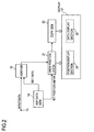
- the input data is compared, on the bit-by-bit basis, against reference data (a series of bit patterns) from a reference data generator 14 in a verifier 15 in order to detect an anticoincidence bit.
- the reference data generator 14 is generally arranged in the same manner as the test data generator 11 to generate the reference data in synchronism with the input data from the input terminal 13.
- the verifier 15 may comprise an exclusive logical sum circuit, for example, which provides an output of logical "1" for each anti coincidence bit between the input data and the reference data.
- bit error position as well as bits in the reference data which precede and follow the error bit can be known, allowing an estimate on what bit pattern is likely to cause an error to be rendered on the basis of the reference data.
- bits in the reference data which are displayed are only those which are located adjacent to the bit error position. In practice, however, it is recognized from the analysis of occurrence of bit errors that a bit pattern status which far precedes the bit error in the test data may have an influence upon the occurrence of the bit error, and in this respect, the conventional apparatus as shown in Fig. 2 fails to elucidate the cause of the bit error.
- the information representing the position of a bit error is displayed in a time sequence in the order it is recorded.
- a bit pattern in the reference data or the input data is continuously displayed, and an error indication mark is applied to a bit in the input data which is subject to an error on the basis of the recorded bit error position information.
- the bit pattern in the reference data or the input data is continuously displayed together with an indication of presence or absence of bit error for each bit.
- a number of error bits and/or bit error rate is determined for each given number of fractional patterns in the reference data, and a relationship between each fraction pattern and the number of bit errors and/or bit error rate is displayed.
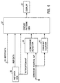
- the coincidence detector 39 constitutes means which determines an error bit in the input data on the basis of the error bit position information fed from the terminal 38.
- the reference data generator 36 may be replaced by the reference data generator 14. Alternatively, the reference data generator may be implemented in a software.
- the data processor 32 may use a number of errors calculator 48 which calculates the number of errors for each bit position by performing the procedure shown in Fig. 8, in place of the error bit counter 41 shown in Fig. 6. If desired, the calculator 48 may calculate a bit error rate. Rather than displaying the bit on the pattern display section 33 shown in Fig. 7 in different colors depending on the bit error rate, the bit may be displayed in different colors depending on the number of errors which prevails at that bit position. To provide a display on the display sections 44 to 46 as illustrated in Fig. 7, bit position designation information which designates the bit position by a marker is also input to the display pattern generator 37.
- the function of the data processor 32 may be performed by allowing a computer to execute a corresponding program.
- a memory 75 which stores a program for calculating a number of errors and an error rate and an input section 30 are connected to the bus 74, as indicated in broken lines in Fig. 23, and the display program stored in the memory 71 is prepared to provide the display illustrated in Fig. 7.
- a switching indicator (the number of times a bit changes or a change rate) may be determined for a given number of the bits in the reference data, for example, every 32 or 64 bit, and the switching rate may be repeatedly determined while sequentially displacing the group by one bit or a plurality of bits, thus providing the switching indicator as a curve 52.
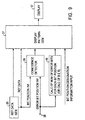
- a data processor 32 which provides the display as shown in Fig. 10 may be arranged as shown in Fig. 11, for example.
- a mark ratio calculator 53 calculates the mark ratio for the group of given bits in the reference data which is supplied from the reference data generator 36 and repeats the calculation while displacing the group by one bit, and the result is fed to the displaying pattern generator 37.
- a switching indicator calculator 54 determines the switching indicator for the given bit group in the reference data and such calculation is repeated while sequentially displacing the group by one bit, and the result is fed to the display pattern generator 37.
- the calculator 48 determines the number of errors or the bit error rate for each position and feeds it to the display pattern generator 37. If required, the bit position information from the reference data generator 36 is also fed to the display pattern generator 37.
- the storage for counting the number of errors for each bit position as described above in connection with Fig. 8 is contained in the calculator 48 which determines the number of error bits for each bit position.
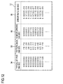
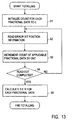
- a data processor 32 which determines the number of error bits or the bit error rate for each fractional data may be arranged as shown in Fig. 14, for example. Specifically, reference data from the reference data generator 36 is fed to the display pattern generator 37. Bit position information from the reference data generator 36 and the error bit position information which is read from the terminal 38 are input to a calculator 58 which calculates the number of error bits for each fractional data. The calculator 58 executes the processing operation illustrated in Fig. 13, and the error bit count for each fractional data, and the bit error rate if required are input to the display pattern generator 37 to provide a display as shown in Fig. 12 on the display 17.
- the bit position information from the reference data generator 36 is input to the calculator 58 which calculates the error bit count for each fractional data to relate each position to some fractional data.
- the store described above in connection with Fig. 12 and which is used to count the error bit count for each fractional data is provided within the calculator 58 which determines the error bit count for each fractional data.
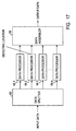
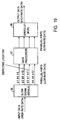
- the input data as shown in Fig. 18 may be input to a slow-down unit (demultiplexer) 66 to distribute the individual bits sequentially to four output lines in a repeated manner, thus converting the input data into a first to a fourth parallel low rate data or four fractional data 62-1 to 62-4, which are then processed in a data processor 67, and the processed first to fourth parallel low rate data are multiplexed into a single high rate data in a multiplexer 68 for purpose of delivery. In this manner, a complicated processing operation can be performed at a lower rate in the data processor 67.
- a slow-down unit (demultiplexer) 66 to distribute the individual bits sequentially to four output lines in a repeated manner, thus converting the input data into a first to a fourth parallel low rate data or four fractional data 62-1 to 62-4, which are then processed in a data processor 67, and the processed first to fourth parallel low rate data are multiplexed into a single high rate data in a multiplexer 68 for purpose of delivery.
- a characteristic polynomial is applied to a given pattern repeatedly until a pattern which coincides with the error bit position information appears, and the number of calculations is chosen as representing the bit position information.
- a technique which determines the phase difference of M-series from the given pattern and the content of the shift register may be used. Where the obtained error bit position information is in the form of a phase difference from a given pattern, that value is displayed as the bit position information.
- information representing the position of an error bit is continuously recorded. Accordingly, a distribution of error bit positions on the bit stream of the reference data can be known from the observation of the error bit position information. For example, when bit errors occur in a burst manner, this can be recognized immediately, and where on the bit stream it occurred can be known.
- the display shown in Fig. 12 allows the error bit count and the bit error rate to be known for each fractional pattern in the reference data.
Landscapes
- Engineering & Computer Science (AREA)
- Computer Networks & Wireless Communication (AREA)
- Signal Processing (AREA)
- Quality & Reliability (AREA)
- Detection And Prevention Of Errors In Transmission (AREA)
- Testing, Inspecting, Measuring Of Stereoscopic Televisions And Televisions (AREA)
Applications Claiming Priority (2)
| Application Number | Priority Date | Filing Date | Title |
|---|---|---|---|
| JP28516999 | 1999-10-06 | ||
| JP28516999A JP4422251B2 (ja) | 1999-10-06 | 1999-10-06 | ビット誤り測定器 |
Publications (2)
| Publication Number | Publication Date |
|---|---|
| EP1091518A2 true EP1091518A2 (fr) | 2001-04-11 |
| EP1091518A3 EP1091518A3 (fr) | 2002-06-26 |
Family
ID=17688003
Family Applications (1)
| Application Number | Title | Priority Date | Filing Date |
|---|---|---|---|
| EP00121289A Withdrawn EP1091518A3 (fr) | 1999-10-06 | 2000-10-06 | Système et procédé pour la mesure d'erreurs de bits |
Country Status (2)
| Country | Link |
|---|---|
| EP (1) | EP1091518A3 (fr) |
| JP (1) | JP4422251B2 (fr) |
Cited By (2)
| Publication number | Priority date | Publication date | Assignee | Title |
|---|---|---|---|---|
| EP2472508A3 (fr) * | 2010-12-28 | 2014-05-14 | Silicon Works Co., Ltd. | Appareil et procédé pour la transmission de données |
| EP2890037A1 (fr) * | 2013-12-31 | 2015-07-01 | General Electric Company | Système de transmission, système de détection et de correction d'erreur et procédé |
Families Citing this family (8)
| Publication number | Priority date | Publication date | Assignee | Title |
|---|---|---|---|---|
| JP4662478B2 (ja) * | 2006-03-31 | 2011-03-30 | アンリツ株式会社 | ビット誤り測定装置 |
| DE112007000761T5 (de) * | 2006-03-31 | 2009-04-02 | Anritsu Corp., Atsugi | Signalanalysevorrichtung |
| JP4992623B2 (ja) * | 2007-09-14 | 2012-08-08 | ソニー株式会社 | 送信装置、送信方法、情報処理装置、情報処理方法、及び、プログラム |
| JP5121480B2 (ja) * | 2008-02-01 | 2013-01-16 | 三菱電機株式会社 | 通信解析装置および通信解析方法 |
| JP4597209B2 (ja) * | 2008-04-14 | 2010-12-15 | 三菱電機株式会社 | 通信解析装置 |
| ES2696511T3 (es) | 2008-02-01 | 2019-01-16 | Mitsubishi Electric Corp | Aparato de análisis de comunicación |
| JP5027277B2 (ja) * | 2010-04-28 | 2012-09-19 | 三菱電機株式会社 | 表示器 |
| JP7046881B2 (ja) * | 2019-10-25 | 2022-04-04 | アンリツ株式会社 | 誤り率測定装置及び誤り率測定方法 |
Family Cites Families (2)
| Publication number | Priority date | Publication date | Assignee | Title |
|---|---|---|---|---|
| DE3733278A1 (de) * | 1987-09-29 | 1989-04-13 | Siemens Ag | Messverfahren zur stoerungsanalyse digitaler uebertragungswege und messeinrichtung zur durchfuehrung des messverfahrens |
| GB2281136B (en) * | 1993-08-11 | 1997-09-24 | Hewlett Packard Ltd | Bit error-rate testing |
-
1999
- 1999-10-06 JP JP28516999A patent/JP4422251B2/ja not_active Expired - Fee Related
-
2000
- 2000-10-06 EP EP00121289A patent/EP1091518A3/fr not_active Withdrawn
Cited By (4)
| Publication number | Priority date | Publication date | Assignee | Title |
|---|---|---|---|---|
| EP2472508A3 (fr) * | 2010-12-28 | 2014-05-14 | Silicon Works Co., Ltd. | Appareil et procédé pour la transmission de données |
| US8775879B2 (en) | 2010-12-28 | 2014-07-08 | Silicon Works Co., Ltd. | Method and apparatus for transmitting data between timing controller and source driver, having bit error rate test function |
| EP2890037A1 (fr) * | 2013-12-31 | 2015-07-01 | General Electric Company | Système de transmission, système de détection et de correction d'erreur et procédé |
| US9374194B2 (en) | 2013-12-31 | 2016-06-21 | General Electric Company | Transmission system error detection and correction system and method |
Also Published As
| Publication number | Publication date |
|---|---|
| JP4422251B2 (ja) | 2010-02-24 |
| JP2001111531A (ja) | 2001-04-20 |
| EP1091518A3 (fr) | 2002-06-26 |
Similar Documents
| Publication | Publication Date | Title |
|---|---|---|
| EP1091518A2 (fr) | Système et procédé pour la mesure d'erreurs de bits | |
| EP0082535B1 (fr) | Appareil pour mesurer et détecter des signaux indésirables | |
| US11379331B2 (en) | Error rate measuring apparatus and error counting method | |
| JP7381533B2 (ja) | 誤り率測定装置及びUncorrectableコードワード検索方法 | |
| US20040078693A1 (en) | Software testing | |
| MY126753A (en) | Automatic measuring apparatus, automatic measurement data processing and control apparatus, network system, and recording medium of automatic measurement processing and control program that selects from a plurality of test conditions | |
| JP7381532B2 (ja) | 誤り率測定装置及びコードワードエラー表示方法 | |
| US8074127B2 (en) | Signal analyzing apparatus | |
| JP7579368B2 (ja) | 誤り率測定装置及び誤り率測定方法 | |
| US20130083686A1 (en) | Systems and Methods of Measuring Communication Performance | |
| EP0939368A1 (fr) | Débogage de programme | |
| KR920008585A (ko) | 비데오 컨트롤러 테스트 장치 및 방법 | |
| JP3993992B2 (ja) | ビットエラー位置測定法のビット値検査法 | |
| JP4061634B2 (ja) | 波形測定器 | |
| US7076739B2 (en) | Data computation apparatus and method for using the data computation apparatus for adjustment of electronic controller | |
| JPH0423634A (ja) | 回線エラーレート監視装置 | |
| US4742445A (en) | Supervisory control computer system of compound generating plant | |
| EP0674458A1 (fr) | Appareil pour la surveillance d'un système ATM | |
| EP1119127A2 (fr) | Dispositif et procédé d'analyse de pointeurs de canaux de signaux SDH | |
| US7890567B2 (en) | Method for determining deviations of an end-system message from a reference message | |
| JP3156750B2 (ja) | 警報発出装置 | |
| JP7579369B2 (ja) | 誤り率測定装置及び誤り率測定方法 | |
| JPH0530224B2 (fr) | ||
| JP3076227B2 (ja) | クロストークエラー検出装置 | |
| KR100800411B1 (ko) | 디지털 비디오 레코더에서의 버퍼 메모리 제어장치 및 방법 |
Legal Events
| Date | Code | Title | Description |
|---|---|---|---|
| PUAI | Public reference made under article 153(3) epc to a published international application that has entered the european phase |
Free format text: ORIGINAL CODE: 0009012 |
|
| 17P | Request for examination filed |
Effective date: 20001006 |
|
| AK | Designated contracting states |
Kind code of ref document: A2 Designated state(s): AT BE CH CY DE DK ES FI FR GB GR IE IT LI LU MC NL PT SE |
|
| AX | Request for extension of the european patent |
Free format text: AL;LT;LV;MK;RO;SI |
|
| PUAL | Search report despatched |
Free format text: ORIGINAL CODE: 0009013 |
|
| AK | Designated contracting states |
Kind code of ref document: A3 Designated state(s): AT BE CH CY DE DK ES FI FR GB GR IE IT LI LU MC NL PT SE |
|
| AX | Request for extension of the european patent |
Free format text: AL;LT;LV;MK;RO;SI |
|
| 17Q | First examination report despatched |
Effective date: 20021210 |
|
| AKX | Designation fees paid |
Designated state(s): DE FR GB |
|
| STAA | Information on the status of an ep patent application or granted ep patent |
Free format text: STATUS: THE APPLICATION IS DEEMED TO BE WITHDRAWN |
|
| 18D | Application deemed to be withdrawn |
Effective date: 20030422 |