EP1096465A2 - Commande d'échelle de gris d'un système d'affichage électro-optique - Google Patents
Commande d'échelle de gris d'un système d'affichage électro-optique Download PDFInfo
- Publication number
- EP1096465A2 EP1096465A2 EP20000123262 EP00123262A EP1096465A2 EP 1096465 A2 EP1096465 A2 EP 1096465A2 EP 20000123262 EP20000123262 EP 20000123262 EP 00123262 A EP00123262 A EP 00123262A EP 1096465 A2 EP1096465 A2 EP 1096465A2
- Authority
- EP
- European Patent Office
- Prior art keywords
- elements
- electro
- optical device
- driver
- electrode
- Prior art date
- Legal status (The legal status is an assumption and is not a legal conclusion. Google has not performed a legal analysis and makes no representation as to the accuracy of the status listed.)
- Granted
Links
- 238000000034 method Methods 0.000 claims description 81
- 230000015654 memory Effects 0.000 claims description 36
- 239000011368 organic material Substances 0.000 claims description 13
- 239000002861 polymer material Substances 0.000 claims description 9
- 238000012937 correction Methods 0.000 claims description 8
- 229920000620 organic polymer Polymers 0.000 claims description 8
- TVIVIEFSHFOWTE-UHFFFAOYSA-K tri(quinolin-8-yloxy)alumane Chemical compound [Al+3].C1=CN=C2C([O-])=CC=CC2=C1.C1=CN=C2C([O-])=CC=CC2=C1.C1=CN=C2C([O-])=CC=CC2=C1 TVIVIEFSHFOWTE-UHFFFAOYSA-K 0.000 claims description 8
- 239000004417 polycarbonate Substances 0.000 claims description 4
- 229920000515 polycarbonate Polymers 0.000 claims description 4
- ODHXBMXNKOYIBV-UHFFFAOYSA-N triphenylamine Chemical compound C1=CC=CC=C1N(C=1C=CC=CC=1)C1=CC=CC=C1 ODHXBMXNKOYIBV-UHFFFAOYSA-N 0.000 claims description 4
- 125000005678 ethenylene group Chemical group [H]C([*:1])=C([H])[*:2] 0.000 claims description 3
- KKFHAJHLJHVUDM-UHFFFAOYSA-N n-vinylcarbazole Chemical compound C1=CC=C2N(C=C)C3=CC=CC=C3C2=C1 KKFHAJHLJHVUDM-UHFFFAOYSA-N 0.000 claims description 3
- 238000005401 electroluminescence Methods 0.000 description 586
- 239000010408 film Substances 0.000 description 163
- 239000010410 layer Substances 0.000 description 151
- 239000003990 capacitor Substances 0.000 description 61
- 239000000463 material Substances 0.000 description 36
- 239000000758 substrate Substances 0.000 description 36
- 238000010586 diagram Methods 0.000 description 35
- 239000012535 impurity Substances 0.000 description 31
- 230000008569 process Effects 0.000 description 23
- 230000015572 biosynthetic process Effects 0.000 description 21
- 239000011229 interlayer Substances 0.000 description 21
- 230000001681 protective effect Effects 0.000 description 20
- 229910052581 Si3N4 Inorganic materials 0.000 description 16
- HQVNEWCFYHHQES-UHFFFAOYSA-N silicon nitride Chemical compound N12[Si]34N5[Si]62N3[Si]51N64 HQVNEWCFYHHQES-UHFFFAOYSA-N 0.000 description 16
- 239000004065 semiconductor Substances 0.000 description 15
- OAICVXFJPJFONN-UHFFFAOYSA-N Phosphorus Chemical compound [P] OAICVXFJPJFONN-UHFFFAOYSA-N 0.000 description 14
- 125000004429 atom Chemical group 0.000 description 14
- 239000011521 glass Substances 0.000 description 14
- 229910052698 phosphorus Inorganic materials 0.000 description 14
- 239000011574 phosphorus Substances 0.000 description 14
- 238000000638 solvent extraction Methods 0.000 description 14
- PXHVJJICTQNCMI-UHFFFAOYSA-N nickel Substances [Ni] PXHVJJICTQNCMI-UHFFFAOYSA-N 0.000 description 13
- 238000002347 injection Methods 0.000 description 12
- 239000007924 injection Substances 0.000 description 12
- VYPSYNLAJGMNEJ-UHFFFAOYSA-N silicon dioxide Inorganic materials O=[Si]=O VYPSYNLAJGMNEJ-UHFFFAOYSA-N 0.000 description 12
- 239000012298 atmosphere Substances 0.000 description 11
- 238000002161 passivation Methods 0.000 description 11
- 238000012545 processing Methods 0.000 description 11
- 238000004020 luminiscence type Methods 0.000 description 10
- 229910021420 polycrystalline silicon Inorganic materials 0.000 description 10
- 229920005591 polysilicon Polymers 0.000 description 10
- 229920005989 resin Polymers 0.000 description 10
- 239000011347 resin Substances 0.000 description 10
- 239000002585 base Substances 0.000 description 9
- 230000001276 controlling effect Effects 0.000 description 9
- 239000006185 dispersion Substances 0.000 description 9
- XUIMIQQOPSSXEZ-UHFFFAOYSA-N Silicon Chemical compound [Si] XUIMIQQOPSSXEZ-UHFFFAOYSA-N 0.000 description 8
- 230000006866 deterioration Effects 0.000 description 8
- 239000011159 matrix material Substances 0.000 description 8
- 229910052710 silicon Inorganic materials 0.000 description 8
- 239000010703 silicon Substances 0.000 description 8
- 229910052814 silicon oxide Inorganic materials 0.000 description 8
- ZOXJGFHDIHLPTG-UHFFFAOYSA-N Boron Chemical compound [B] ZOXJGFHDIHLPTG-UHFFFAOYSA-N 0.000 description 7
- 229910052796 boron Inorganic materials 0.000 description 7
- 238000004519 manufacturing process Methods 0.000 description 7
- 230000003647 oxidation Effects 0.000 description 7
- 238000007254 oxidation reaction Methods 0.000 description 7
- 230000002829 reductive effect Effects 0.000 description 7
- 229910021417 amorphous silicon Inorganic materials 0.000 description 6
- 238000002425 crystallisation Methods 0.000 description 6
- 230000008025 crystallization Effects 0.000 description 6
- 230000003247 decreasing effect Effects 0.000 description 6
- 239000001257 hydrogen Substances 0.000 description 6
- 229910052739 hydrogen Inorganic materials 0.000 description 6
- 150000002500 ions Chemical class 0.000 description 6
- 238000003860 storage Methods 0.000 description 6
- 239000010936 titanium Substances 0.000 description 6
- UFHFLCQGNIYNRP-UHFFFAOYSA-N Hydrogen Chemical compound [H][H] UFHFLCQGNIYNRP-UHFFFAOYSA-N 0.000 description 5
- 229910052783 alkali metal Inorganic materials 0.000 description 5
- 150000001340 alkali metals Chemical class 0.000 description 5
- 238000010438 heat treatment Methods 0.000 description 5
- 238000005984 hydrogenation reaction Methods 0.000 description 5
- 238000003475 lamination Methods 0.000 description 5
- 230000001105 regulatory effect Effects 0.000 description 5
- 238000001771 vacuum deposition Methods 0.000 description 5
- XLYOFNOQVPJJNP-UHFFFAOYSA-N water Substances O XLYOFNOQVPJJNP-UHFFFAOYSA-N 0.000 description 5
- IJGRMHOSHXDMSA-UHFFFAOYSA-N Atomic nitrogen Chemical compound N#N IJGRMHOSHXDMSA-UHFFFAOYSA-N 0.000 description 4
- 229910052782 aluminium Inorganic materials 0.000 description 4
- XAGFODPZIPBFFR-UHFFFAOYSA-N aluminium Chemical compound [Al] XAGFODPZIPBFFR-UHFFFAOYSA-N 0.000 description 4
- QVGXLLKOCUKJST-UHFFFAOYSA-N atomic oxygen Chemical compound [O] QVGXLLKOCUKJST-UHFFFAOYSA-N 0.000 description 4
- QVQLCTNNEUAWMS-UHFFFAOYSA-N barium oxide Chemical compound [Ba]=O QVQLCTNNEUAWMS-UHFFFAOYSA-N 0.000 description 4
- UMIVXZPTRXBADB-UHFFFAOYSA-N benzocyclobutene Chemical compound C1=CC=C2CCC2=C1 UMIVXZPTRXBADB-UHFFFAOYSA-N 0.000 description 4
- 230000000694 effects Effects 0.000 description 4
- 230000005525 hole transport Effects 0.000 description 4
- 239000011777 magnesium Substances 0.000 description 4
- 239000001301 oxygen Substances 0.000 description 4
- 229910052760 oxygen Inorganic materials 0.000 description 4
- 229920000642 polymer Polymers 0.000 description 4
- 239000010453 quartz Substances 0.000 description 4
- 238000000926 separation method Methods 0.000 description 4
- 239000002356 single layer Substances 0.000 description 4
- 238000004544 sputter deposition Methods 0.000 description 4
- 229910052721 tungsten Inorganic materials 0.000 description 4
- 239000010937 tungsten Substances 0.000 description 4
- -1 tungsten nitride Chemical class 0.000 description 4
- 239000004925 Acrylic resin Substances 0.000 description 3
- 206010010144 Completed suicide Diseases 0.000 description 3
- 239000004642 Polyimide Substances 0.000 description 3
- NIXOWILDQLNWCW-UHFFFAOYSA-N acrylic acid group Chemical group C(C=C)(=O)O NIXOWILDQLNWCW-UHFFFAOYSA-N 0.000 description 3
- 238000000137 annealing Methods 0.000 description 3
- 239000003054 catalyst Substances 0.000 description 3
- 239000000919 ceramic Substances 0.000 description 3
- 239000003822 epoxy resin Substances 0.000 description 3
- 229910052751 metal Inorganic materials 0.000 description 3
- 238000000059 patterning Methods 0.000 description 3
- 238000005268 plasma chemical vapour deposition Methods 0.000 description 3
- 229920000647 polyepoxide Polymers 0.000 description 3
- 229920001721 polyimide Polymers 0.000 description 3
- 239000000243 solution Substances 0.000 description 3
- WFKWXMTUELFFGS-UHFFFAOYSA-N tungsten Chemical compound [W] WFKWXMTUELFFGS-UHFFFAOYSA-N 0.000 description 3
- 229920000178 Acrylic resin Polymers 0.000 description 2
- XYFCBTPGUUZFHI-UHFFFAOYSA-N Phosphine Chemical compound P XYFCBTPGUUZFHI-UHFFFAOYSA-N 0.000 description 2
- PPBRXRYQALVLMV-UHFFFAOYSA-N Styrene Chemical compound C=CC1=CC=CC=C1 PPBRXRYQALVLMV-UHFFFAOYSA-N 0.000 description 2
- RTAQQCXQSZGOHL-UHFFFAOYSA-N Titanium Chemical compound [Ti] RTAQQCXQSZGOHL-UHFFFAOYSA-N 0.000 description 2
- 230000003213 activating effect Effects 0.000 description 2
- 230000004913 activation Effects 0.000 description 2
- 229910045601 alloy Inorganic materials 0.000 description 2
- 239000000956 alloy Substances 0.000 description 2
- 238000004458 analytical method Methods 0.000 description 2
- 230000008901 benefit Effects 0.000 description 2
- 230000033228 biological regulation Effects 0.000 description 2
- DQXBYHZEEUGOBF-UHFFFAOYSA-N but-3-enoic acid;ethene Chemical compound C=C.OC(=O)CC=C DQXBYHZEEUGOBF-UHFFFAOYSA-N 0.000 description 2
- 239000011575 calcium Substances 0.000 description 2
- 238000001816 cooling Methods 0.000 description 2
- 239000010949 copper Substances 0.000 description 2
- 239000013078 crystal Substances 0.000 description 2
- 239000002274 desiccant Substances 0.000 description 2
- ZOCHARZZJNPSEU-UHFFFAOYSA-N diboron Chemical compound B#B ZOCHARZZJNPSEU-UHFFFAOYSA-N 0.000 description 2
- 239000002019 doping agent Substances 0.000 description 2
- 239000005038 ethylene vinyl acetate Substances 0.000 description 2
- 230000005284 excitation Effects 0.000 description 2
- 230000006870 function Effects 0.000 description 2
- 239000007789 gas Substances 0.000 description 2
- 238000005468 ion implantation Methods 0.000 description 2
- 238000002955 isolation Methods 0.000 description 2
- 239000004973 liquid crystal related substance Substances 0.000 description 2
- 238000005259 measurement Methods 0.000 description 2
- 239000002184 metal Substances 0.000 description 2
- 229910052759 nickel Inorganic materials 0.000 description 2
- 229910052757 nitrogen Inorganic materials 0.000 description 2
- 238000000206 photolithography Methods 0.000 description 2
- 229920001200 poly(ethylene-vinyl acetate) Polymers 0.000 description 2
- 229920002037 poly(vinyl butyral) polymer Polymers 0.000 description 2
- 239000004800 polyvinyl chloride Substances 0.000 description 2
- 229920000915 polyvinyl chloride Polymers 0.000 description 2
- 229910052709 silver Inorganic materials 0.000 description 2
- 239000010409 thin film Substances 0.000 description 2
- 229910052719 titanium Inorganic materials 0.000 description 2
- YLYPIBBGWLKELC-RMKNXTFCSA-N 2-[2-[(e)-2-[4-(dimethylamino)phenyl]ethenyl]-6-methylpyran-4-ylidene]propanedinitrile Chemical compound C1=CC(N(C)C)=CC=C1\C=C\C1=CC(=C(C#N)C#N)C=C(C)O1 YLYPIBBGWLKELC-RMKNXTFCSA-N 0.000 description 1
- ZPSJGADGUYYRKE-UHFFFAOYSA-N 2H-pyran-2-one Chemical compound O=C1C=CC=CO1 ZPSJGADGUYYRKE-UHFFFAOYSA-N 0.000 description 1
- 229920002972 Acrylic fiber Polymers 0.000 description 1
- OYPRJOBELJOOCE-UHFFFAOYSA-N Calcium Chemical compound [Ca] OYPRJOBELJOOCE-UHFFFAOYSA-N 0.000 description 1
- VYZAMTAEIAYCRO-UHFFFAOYSA-N Chromium Chemical compound [Cr] VYZAMTAEIAYCRO-UHFFFAOYSA-N 0.000 description 1
- RYGMFSIKBFXOCR-UHFFFAOYSA-N Copper Chemical compound [Cu] RYGMFSIKBFXOCR-UHFFFAOYSA-N 0.000 description 1
- GYHNNYVSQQEPJS-UHFFFAOYSA-N Gallium Chemical compound [Ga] GYHNNYVSQQEPJS-UHFFFAOYSA-N 0.000 description 1
- DGAQECJNVWCQMB-PUAWFVPOSA-M Ilexoside XXIX Chemical compound C[C@@H]1CC[C@@]2(CC[C@@]3(C(=CC[C@H]4[C@]3(CC[C@@H]5[C@@]4(CC[C@@H](C5(C)C)OS(=O)(=O)[O-])C)C)[C@@H]2[C@]1(C)O)C)C(=O)O[C@H]6[C@@H]([C@H]([C@@H]([C@H](O6)CO)O)O)O.[Na+] DGAQECJNVWCQMB-PUAWFVPOSA-M 0.000 description 1
- 229910010199 LiAl Inorganic materials 0.000 description 1
- WHXSMMKQMYFTQS-UHFFFAOYSA-N Lithium Chemical compound [Li] WHXSMMKQMYFTQS-UHFFFAOYSA-N 0.000 description 1
- FYYHWMGAXLPEAU-UHFFFAOYSA-N Magnesium Chemical compound [Mg] FYYHWMGAXLPEAU-UHFFFAOYSA-N 0.000 description 1
- ZOKXTWBITQBERF-UHFFFAOYSA-N Molybdenum Chemical compound [Mo] ZOKXTWBITQBERF-UHFFFAOYSA-N 0.000 description 1
- 239000004952 Polyamide Substances 0.000 description 1
- NRCMAYZCPIVABH-UHFFFAOYSA-N Quinacridone Chemical compound N1C2=CC=CC=C2C(=O)C2=C1C=C1C(=O)C3=CC=CC=C3NC1=C2 NRCMAYZCPIVABH-UHFFFAOYSA-N 0.000 description 1
- 229910006992 Si1-xCx Inorganic materials 0.000 description 1
- 229910020286 SiOxNy Inorganic materials 0.000 description 1
- BQCADISMDOOEFD-UHFFFAOYSA-N Silver Chemical compound [Ag] BQCADISMDOOEFD-UHFFFAOYSA-N 0.000 description 1
- 229910001362 Ta alloys Inorganic materials 0.000 description 1
- NRTOMJZYCJJWKI-UHFFFAOYSA-N Titanium nitride Chemical compound [Ti]#N NRTOMJZYCJJWKI-UHFFFAOYSA-N 0.000 description 1
- 229910001080 W alloy Inorganic materials 0.000 description 1
- XLOMVQKBTHCTTD-UHFFFAOYSA-N Zinc monoxide Chemical compound [Zn]=O XLOMVQKBTHCTTD-UHFFFAOYSA-N 0.000 description 1
- LEVVHYCKPQWKOP-UHFFFAOYSA-N [Si].[Ge] Chemical compound [Si].[Ge] LEVVHYCKPQWKOP-UHFFFAOYSA-N 0.000 description 1
- 239000000853 adhesive Substances 0.000 description 1
- 230000001070 adhesive effect Effects 0.000 description 1
- 230000002411 adverse Effects 0.000 description 1
- 229910052785 arsenic Inorganic materials 0.000 description 1
- RQNWIZPPADIBDY-UHFFFAOYSA-N arsenic atom Chemical compound [As] RQNWIZPPADIBDY-UHFFFAOYSA-N 0.000 description 1
- IVHJCRXBQPGLOV-UHFFFAOYSA-N azanylidynetungsten Chemical compound [W]#N IVHJCRXBQPGLOV-UHFFFAOYSA-N 0.000 description 1
- 239000005388 borosilicate glass Substances 0.000 description 1
- 229910052791 calcium Inorganic materials 0.000 description 1
- 239000000969 carrier Substances 0.000 description 1
- 230000008859 change Effects 0.000 description 1
- 238000006243 chemical reaction Methods 0.000 description 1
- 239000003086 colorant Substances 0.000 description 1
- 238000004040 coloring Methods 0.000 description 1
- 150000001875 compounds Chemical class 0.000 description 1
- 239000000470 constituent Substances 0.000 description 1
- 229910052802 copper Inorganic materials 0.000 description 1
- 230000007547 defect Effects 0.000 description 1
- 238000011161 development Methods 0.000 description 1
- 238000007598 dipping method Methods 0.000 description 1
- 230000005685 electric field effect Effects 0.000 description 1
- 238000005516 engineering process Methods 0.000 description 1
- 238000005530 etching Methods 0.000 description 1
- 229910052733 gallium Inorganic materials 0.000 description 1
- 230000007274 generation of a signal involved in cell-cell signaling Effects 0.000 description 1
- 238000005247 gettering Methods 0.000 description 1
- 239000002241 glass-ceramic Substances 0.000 description 1
- 229910052736 halogen Inorganic materials 0.000 description 1
- 150000002367 halogens Chemical class 0.000 description 1
- 150000002431 hydrogen Chemical class 0.000 description 1
- 229910003437 indium oxide Inorganic materials 0.000 description 1
- PJXISJQVUVHSOJ-UHFFFAOYSA-N indium(iii) oxide Chemical compound [O-2].[O-2].[O-2].[In+3].[In+3] PJXISJQVUVHSOJ-UHFFFAOYSA-N 0.000 description 1
- AMGQUBHHOARCQH-UHFFFAOYSA-N indium;oxotin Chemical compound [In].[Sn]=O AMGQUBHHOARCQH-UHFFFAOYSA-N 0.000 description 1
- 239000011261 inert gas Substances 0.000 description 1
- 238000007641 inkjet printing Methods 0.000 description 1
- 229910010272 inorganic material Inorganic materials 0.000 description 1
- 239000011147 inorganic material Substances 0.000 description 1
- 239000011810 insulating material Substances 0.000 description 1
- 238000007733 ion plating Methods 0.000 description 1
- 239000005001 laminate film Substances 0.000 description 1
- 229910052744 lithium Inorganic materials 0.000 description 1
- 238000002796 luminescence method Methods 0.000 description 1
- 229910052749 magnesium Inorganic materials 0.000 description 1
- 239000003550 marker Substances 0.000 description 1
- 239000007769 metal material Substances 0.000 description 1
- 239000013081 microcrystal Substances 0.000 description 1
- 239000000203 mixture Substances 0.000 description 1
- 229910052750 molybdenum Inorganic materials 0.000 description 1
- 239000011733 molybdenum Substances 0.000 description 1
- VOFUROIFQGPCGE-UHFFFAOYSA-N nile red Chemical compound C1=CC=C2C3=NC4=CC=C(N(CC)CC)C=C4OC3=CC(=O)C2=C1 VOFUROIFQGPCGE-UHFFFAOYSA-N 0.000 description 1
- 150000004767 nitrides Chemical class 0.000 description 1
- 239000012299 nitrogen atmosphere Substances 0.000 description 1
- 230000003287 optical effect Effects 0.000 description 1
- 230000001590 oxidative effect Effects 0.000 description 1
- 230000003071 parasitic effect Effects 0.000 description 1
- 238000005192 partition Methods 0.000 description 1
- 238000009832 plasma treatment Methods 0.000 description 1
- 229920003227 poly(N-vinyl carbazole) Polymers 0.000 description 1
- 229920000553 poly(phenylenevinylene) Polymers 0.000 description 1
- 229920002647 polyamide Polymers 0.000 description 1
- 229920005668 polycarbonate resin Polymers 0.000 description 1
- 239000004431 polycarbonate resin Substances 0.000 description 1
- 238000007639 printing Methods 0.000 description 1
- 239000011241 protective layer Substances 0.000 description 1
- 230000006798 recombination Effects 0.000 description 1
- 238000005215 recombination Methods 0.000 description 1
- 238000011160 research Methods 0.000 description 1
- 238000012827 research and development Methods 0.000 description 1
- 230000004044 response Effects 0.000 description 1
- 230000000452 restraining effect Effects 0.000 description 1
- 230000002441 reversible effect Effects 0.000 description 1
- 238000007650 screen-printing Methods 0.000 description 1
- 238000007789 sealing Methods 0.000 description 1
- 229920002050 silicone resin Polymers 0.000 description 1
- 239000004332 silver Substances 0.000 description 1
- 238000009751 slip forming Methods 0.000 description 1
- 229910052708 sodium Inorganic materials 0.000 description 1
- 239000011734 sodium Substances 0.000 description 1
- 238000004528 spin coating Methods 0.000 description 1
- 238000005728 strengthening Methods 0.000 description 1
- 239000000126 substance Substances 0.000 description 1
- 229910052715 tantalum Inorganic materials 0.000 description 1
- GUVRBAGPIYLISA-UHFFFAOYSA-N tantalum atom Chemical compound [Ta] GUVRBAGPIYLISA-UHFFFAOYSA-N 0.000 description 1
- MZLGASXMSKOWSE-UHFFFAOYSA-N tantalum nitride Chemical compound [Ta]#N MZLGASXMSKOWSE-UHFFFAOYSA-N 0.000 description 1
- 229920001187 thermosetting polymer Polymers 0.000 description 1
- 239000012808 vapor phase Substances 0.000 description 1
- 238000001039 wet etching Methods 0.000 description 1
Images






Classifications
-
- G—PHYSICS
- G09—EDUCATION; CRYPTOGRAPHY; DISPLAY; ADVERTISING; SEALS
- G09G—ARRANGEMENTS OR CIRCUITS FOR CONTROL OF INDICATING DEVICES USING STATIC MEANS TO PRESENT VARIABLE INFORMATION
- G09G3/00—Control arrangements or circuits, of interest only in connection with visual indicators other than cathode-ray tubes
- G09G3/20—Control arrangements or circuits, of interest only in connection with visual indicators other than cathode-ray tubes for presentation of an assembly of a number of characters, e.g. a page, by composing the assembly by combination of individual elements arranged in a matrix no fixed position being assigned to or needed to be assigned to the individual characters or partial characters
- G09G3/22—Control arrangements or circuits, of interest only in connection with visual indicators other than cathode-ray tubes for presentation of an assembly of a number of characters, e.g. a page, by composing the assembly by combination of individual elements arranged in a matrix no fixed position being assigned to or needed to be assigned to the individual characters or partial characters using controlled light sources
- G09G3/30—Control arrangements or circuits, of interest only in connection with visual indicators other than cathode-ray tubes for presentation of an assembly of a number of characters, e.g. a page, by composing the assembly by combination of individual elements arranged in a matrix no fixed position being assigned to or needed to be assigned to the individual characters or partial characters using controlled light sources using electroluminescent panels
-
- G—PHYSICS
- G09—EDUCATION; CRYPTOGRAPHY; DISPLAY; ADVERTISING; SEALS
- G09G—ARRANGEMENTS OR CIRCUITS FOR CONTROL OF INDICATING DEVICES USING STATIC MEANS TO PRESENT VARIABLE INFORMATION
- G09G3/00—Control arrangements or circuits, of interest only in connection with visual indicators other than cathode-ray tubes
- G09G3/20—Control arrangements or circuits, of interest only in connection with visual indicators other than cathode-ray tubes for presentation of an assembly of a number of characters, e.g. a page, by composing the assembly by combination of individual elements arranged in a matrix no fixed position being assigned to or needed to be assigned to the individual characters or partial characters
- G09G3/2007—Display of intermediate tones
- G09G3/2018—Display of intermediate tones by time modulation using two or more time intervals
- G09G3/2022—Display of intermediate tones by time modulation using two or more time intervals using sub-frames
-
- G—PHYSICS
- G09—EDUCATION; CRYPTOGRAPHY; DISPLAY; ADVERTISING; SEALS
- G09G—ARRANGEMENTS OR CIRCUITS FOR CONTROL OF INDICATING DEVICES USING STATIC MEANS TO PRESENT VARIABLE INFORMATION
- G09G3/00—Control arrangements or circuits, of interest only in connection with visual indicators other than cathode-ray tubes
- G09G3/20—Control arrangements or circuits, of interest only in connection with visual indicators other than cathode-ray tubes for presentation of an assembly of a number of characters, e.g. a page, by composing the assembly by combination of individual elements arranged in a matrix no fixed position being assigned to or needed to be assigned to the individual characters or partial characters
- G09G3/2007—Display of intermediate tones
- G09G3/2077—Display of intermediate tones by a combination of two or more gradation control methods
-
- G—PHYSICS
- G09—EDUCATION; CRYPTOGRAPHY; DISPLAY; ADVERTISING; SEALS
- G09G—ARRANGEMENTS OR CIRCUITS FOR CONTROL OF INDICATING DEVICES USING STATIC MEANS TO PRESENT VARIABLE INFORMATION
- G09G3/00—Control arrangements or circuits, of interest only in connection with visual indicators other than cathode-ray tubes
- G09G3/20—Control arrangements or circuits, of interest only in connection with visual indicators other than cathode-ray tubes for presentation of an assembly of a number of characters, e.g. a page, by composing the assembly by combination of individual elements arranged in a matrix no fixed position being assigned to or needed to be assigned to the individual characters or partial characters
- G09G3/22—Control arrangements or circuits, of interest only in connection with visual indicators other than cathode-ray tubes for presentation of an assembly of a number of characters, e.g. a page, by composing the assembly by combination of individual elements arranged in a matrix no fixed position being assigned to or needed to be assigned to the individual characters or partial characters using controlled light sources
- G09G3/30—Control arrangements or circuits, of interest only in connection with visual indicators other than cathode-ray tubes for presentation of an assembly of a number of characters, e.g. a page, by composing the assembly by combination of individual elements arranged in a matrix no fixed position being assigned to or needed to be assigned to the individual characters or partial characters using controlled light sources using electroluminescent panels
- G09G3/32—Control arrangements or circuits, of interest only in connection with visual indicators other than cathode-ray tubes for presentation of an assembly of a number of characters, e.g. a page, by composing the assembly by combination of individual elements arranged in a matrix no fixed position being assigned to or needed to be assigned to the individual characters or partial characters using controlled light sources using electroluminescent panels semiconductive, e.g. using light-emitting diodes [LED]
- G09G3/3208—Control arrangements or circuits, of interest only in connection with visual indicators other than cathode-ray tubes for presentation of an assembly of a number of characters, e.g. a page, by composing the assembly by combination of individual elements arranged in a matrix no fixed position being assigned to or needed to be assigned to the individual characters or partial characters using controlled light sources using electroluminescent panels semiconductive, e.g. using light-emitting diodes [LED] organic, e.g. using organic light-emitting diodes [OLED]
- G09G3/3225—Control arrangements or circuits, of interest only in connection with visual indicators other than cathode-ray tubes for presentation of an assembly of a number of characters, e.g. a page, by composing the assembly by combination of individual elements arranged in a matrix no fixed position being assigned to or needed to be assigned to the individual characters or partial characters using controlled light sources using electroluminescent panels semiconductive, e.g. using light-emitting diodes [LED] organic, e.g. using organic light-emitting diodes [OLED] using an active matrix
- G09G3/3233—Control arrangements or circuits, of interest only in connection with visual indicators other than cathode-ray tubes for presentation of an assembly of a number of characters, e.g. a page, by composing the assembly by combination of individual elements arranged in a matrix no fixed position being assigned to or needed to be assigned to the individual characters or partial characters using controlled light sources using electroluminescent panels semiconductive, e.g. using light-emitting diodes [LED] organic, e.g. using organic light-emitting diodes [OLED] using an active matrix with pixel circuitry controlling the current through the light-emitting element
-
- G—PHYSICS
- G09—EDUCATION; CRYPTOGRAPHY; DISPLAY; ADVERTISING; SEALS
- G09G—ARRANGEMENTS OR CIRCUITS FOR CONTROL OF INDICATING DEVICES USING STATIC MEANS TO PRESENT VARIABLE INFORMATION
- G09G3/00—Control arrangements or circuits, of interest only in connection with visual indicators other than cathode-ray tubes
- G09G3/20—Control arrangements or circuits, of interest only in connection with visual indicators other than cathode-ray tubes for presentation of an assembly of a number of characters, e.g. a page, by composing the assembly by combination of individual elements arranged in a matrix no fixed position being assigned to or needed to be assigned to the individual characters or partial characters
- G09G3/22—Control arrangements or circuits, of interest only in connection with visual indicators other than cathode-ray tubes for presentation of an assembly of a number of characters, e.g. a page, by composing the assembly by combination of individual elements arranged in a matrix no fixed position being assigned to or needed to be assigned to the individual characters or partial characters using controlled light sources
- G09G3/30—Control arrangements or circuits, of interest only in connection with visual indicators other than cathode-ray tubes for presentation of an assembly of a number of characters, e.g. a page, by composing the assembly by combination of individual elements arranged in a matrix no fixed position being assigned to or needed to be assigned to the individual characters or partial characters using controlled light sources using electroluminescent panels
- G09G3/32—Control arrangements or circuits, of interest only in connection with visual indicators other than cathode-ray tubes for presentation of an assembly of a number of characters, e.g. a page, by composing the assembly by combination of individual elements arranged in a matrix no fixed position being assigned to or needed to be assigned to the individual characters or partial characters using controlled light sources using electroluminescent panels semiconductive, e.g. using light-emitting diodes [LED]
- G09G3/3208—Control arrangements or circuits, of interest only in connection with visual indicators other than cathode-ray tubes for presentation of an assembly of a number of characters, e.g. a page, by composing the assembly by combination of individual elements arranged in a matrix no fixed position being assigned to or needed to be assigned to the individual characters or partial characters using controlled light sources using electroluminescent panels semiconductive, e.g. using light-emitting diodes [LED] organic, e.g. using organic light-emitting diodes [OLED]
- G09G3/3225—Control arrangements or circuits, of interest only in connection with visual indicators other than cathode-ray tubes for presentation of an assembly of a number of characters, e.g. a page, by composing the assembly by combination of individual elements arranged in a matrix no fixed position being assigned to or needed to be assigned to the individual characters or partial characters using controlled light sources using electroluminescent panels semiconductive, e.g. using light-emitting diodes [LED] organic, e.g. using organic light-emitting diodes [OLED] using an active matrix
- G09G3/3258—Control arrangements or circuits, of interest only in connection with visual indicators other than cathode-ray tubes for presentation of an assembly of a number of characters, e.g. a page, by composing the assembly by combination of individual elements arranged in a matrix no fixed position being assigned to or needed to be assigned to the individual characters or partial characters using controlled light sources using electroluminescent panels semiconductive, e.g. using light-emitting diodes [LED] organic, e.g. using organic light-emitting diodes [OLED] using an active matrix with pixel circuitry controlling the voltage across the light-emitting element
-
- G—PHYSICS
- G09—EDUCATION; CRYPTOGRAPHY; DISPLAY; ADVERTISING; SEALS
- G09G—ARRANGEMENTS OR CIRCUITS FOR CONTROL OF INDICATING DEVICES USING STATIC MEANS TO PRESENT VARIABLE INFORMATION
- G09G3/00—Control arrangements or circuits, of interest only in connection with visual indicators other than cathode-ray tubes
- G09G3/20—Control arrangements or circuits, of interest only in connection with visual indicators other than cathode-ray tubes for presentation of an assembly of a number of characters, e.g. a page, by composing the assembly by combination of individual elements arranged in a matrix no fixed position being assigned to or needed to be assigned to the individual characters or partial characters
- G09G3/22—Control arrangements or circuits, of interest only in connection with visual indicators other than cathode-ray tubes for presentation of an assembly of a number of characters, e.g. a page, by composing the assembly by combination of individual elements arranged in a matrix no fixed position being assigned to or needed to be assigned to the individual characters or partial characters using controlled light sources
- G09G3/30—Control arrangements or circuits, of interest only in connection with visual indicators other than cathode-ray tubes for presentation of an assembly of a number of characters, e.g. a page, by composing the assembly by combination of individual elements arranged in a matrix no fixed position being assigned to or needed to be assigned to the individual characters or partial characters using controlled light sources using electroluminescent panels
- G09G3/32—Control arrangements or circuits, of interest only in connection with visual indicators other than cathode-ray tubes for presentation of an assembly of a number of characters, e.g. a page, by composing the assembly by combination of individual elements arranged in a matrix no fixed position being assigned to or needed to be assigned to the individual characters or partial characters using controlled light sources using electroluminescent panels semiconductive, e.g. using light-emitting diodes [LED]
- G09G3/3208—Control arrangements or circuits, of interest only in connection with visual indicators other than cathode-ray tubes for presentation of an assembly of a number of characters, e.g. a page, by composing the assembly by combination of individual elements arranged in a matrix no fixed position being assigned to or needed to be assigned to the individual characters or partial characters using controlled light sources using electroluminescent panels semiconductive, e.g. using light-emitting diodes [LED] organic, e.g. using organic light-emitting diodes [OLED]
- G09G3/3266—Details of drivers for scan electrodes
-
- G—PHYSICS
- G09—EDUCATION; CRYPTOGRAPHY; DISPLAY; ADVERTISING; SEALS
- G09G—ARRANGEMENTS OR CIRCUITS FOR CONTROL OF INDICATING DEVICES USING STATIC MEANS TO PRESENT VARIABLE INFORMATION
- G09G3/00—Control arrangements or circuits, of interest only in connection with visual indicators other than cathode-ray tubes
- G09G3/20—Control arrangements or circuits, of interest only in connection with visual indicators other than cathode-ray tubes for presentation of an assembly of a number of characters, e.g. a page, by composing the assembly by combination of individual elements arranged in a matrix no fixed position being assigned to or needed to be assigned to the individual characters or partial characters
- G09G3/22—Control arrangements or circuits, of interest only in connection with visual indicators other than cathode-ray tubes for presentation of an assembly of a number of characters, e.g. a page, by composing the assembly by combination of individual elements arranged in a matrix no fixed position being assigned to or needed to be assigned to the individual characters or partial characters using controlled light sources
- G09G3/30—Control arrangements or circuits, of interest only in connection with visual indicators other than cathode-ray tubes for presentation of an assembly of a number of characters, e.g. a page, by composing the assembly by combination of individual elements arranged in a matrix no fixed position being assigned to or needed to be assigned to the individual characters or partial characters using controlled light sources using electroluminescent panels
- G09G3/32—Control arrangements or circuits, of interest only in connection with visual indicators other than cathode-ray tubes for presentation of an assembly of a number of characters, e.g. a page, by composing the assembly by combination of individual elements arranged in a matrix no fixed position being assigned to or needed to be assigned to the individual characters or partial characters using controlled light sources using electroluminescent panels semiconductive, e.g. using light-emitting diodes [LED]
- G09G3/3208—Control arrangements or circuits, of interest only in connection with visual indicators other than cathode-ray tubes for presentation of an assembly of a number of characters, e.g. a page, by composing the assembly by combination of individual elements arranged in a matrix no fixed position being assigned to or needed to be assigned to the individual characters or partial characters using controlled light sources using electroluminescent panels semiconductive, e.g. using light-emitting diodes [LED] organic, e.g. using organic light-emitting diodes [OLED]
- G09G3/3275—Details of drivers for data electrodes
-
- G—PHYSICS
- G09—EDUCATION; CRYPTOGRAPHY; DISPLAY; ADVERTISING; SEALS
- G09G—ARRANGEMENTS OR CIRCUITS FOR CONTROL OF INDICATING DEVICES USING STATIC MEANS TO PRESENT VARIABLE INFORMATION
- G09G3/00—Control arrangements or circuits, of interest only in connection with visual indicators other than cathode-ray tubes
- G09G3/20—Control arrangements or circuits, of interest only in connection with visual indicators other than cathode-ray tubes for presentation of an assembly of a number of characters, e.g. a page, by composing the assembly by combination of individual elements arranged in a matrix no fixed position being assigned to or needed to be assigned to the individual characters or partial characters
- G09G3/22—Control arrangements or circuits, of interest only in connection with visual indicators other than cathode-ray tubes for presentation of an assembly of a number of characters, e.g. a page, by composing the assembly by combination of individual elements arranged in a matrix no fixed position being assigned to or needed to be assigned to the individual characters or partial characters using controlled light sources
- G09G3/30—Control arrangements or circuits, of interest only in connection with visual indicators other than cathode-ray tubes for presentation of an assembly of a number of characters, e.g. a page, by composing the assembly by combination of individual elements arranged in a matrix no fixed position being assigned to or needed to be assigned to the individual characters or partial characters using controlled light sources using electroluminescent panels
- G09G3/32—Control arrangements or circuits, of interest only in connection with visual indicators other than cathode-ray tubes for presentation of an assembly of a number of characters, e.g. a page, by composing the assembly by combination of individual elements arranged in a matrix no fixed position being assigned to or needed to be assigned to the individual characters or partial characters using controlled light sources using electroluminescent panels semiconductive, e.g. using light-emitting diodes [LED]
- G09G3/3208—Control arrangements or circuits, of interest only in connection with visual indicators other than cathode-ray tubes for presentation of an assembly of a number of characters, e.g. a page, by composing the assembly by combination of individual elements arranged in a matrix no fixed position being assigned to or needed to be assigned to the individual characters or partial characters using controlled light sources using electroluminescent panels semiconductive, e.g. using light-emitting diodes [LED] organic, e.g. using organic light-emitting diodes [OLED]
- G09G3/3275—Details of drivers for data electrodes
- G09G3/3291—Details of drivers for data electrodes in which the data driver supplies a variable data voltage for setting the current through, or the voltage across, the light-emitting elements
-
- H—ELECTRICITY
- H10—SEMICONDUCTOR DEVICES; ELECTRIC SOLID-STATE DEVICES NOT OTHERWISE PROVIDED FOR
- H10D—INORGANIC ELECTRIC SEMICONDUCTOR DEVICES
- H10D30/00—Field-effect transistors [FET]
- H10D30/60—Insulated-gate field-effect transistors [IGFET]
- H10D30/67—Thin-film transistors [TFT]
- H10D30/674—Thin-film transistors [TFT] characterised by the active materials
- H10D30/6741—Group IV materials, e.g. germanium or silicon carbide
- H10D30/6743—Silicon
- H10D30/6745—Polycrystalline or microcrystalline silicon
-
- H—ELECTRICITY
- H10—SEMICONDUCTOR DEVICES; ELECTRIC SOLID-STATE DEVICES NOT OTHERWISE PROVIDED FOR
- H10D—INORGANIC ELECTRIC SEMICONDUCTOR DEVICES
- H10D86/00—Integrated devices formed in or on insulating or conducting substrates, e.g. formed in silicon-on-insulator [SOI] substrates or on stainless steel or glass substrates
- H10D86/40—Integrated devices formed in or on insulating or conducting substrates, e.g. formed in silicon-on-insulator [SOI] substrates or on stainless steel or glass substrates characterised by multiple TFTs
-
- H—ELECTRICITY
- H10—SEMICONDUCTOR DEVICES; ELECTRIC SOLID-STATE DEVICES NOT OTHERWISE PROVIDED FOR
- H10D—INORGANIC ELECTRIC SEMICONDUCTOR DEVICES
- H10D86/00—Integrated devices formed in or on insulating or conducting substrates, e.g. formed in silicon-on-insulator [SOI] substrates or on stainless steel or glass substrates
- H10D86/40—Integrated devices formed in or on insulating or conducting substrates, e.g. formed in silicon-on-insulator [SOI] substrates or on stainless steel or glass substrates characterised by multiple TFTs
- H10D86/451—Integrated devices formed in or on insulating or conducting substrates, e.g. formed in silicon-on-insulator [SOI] substrates or on stainless steel or glass substrates characterised by multiple TFTs characterised by the compositions or shapes of the interlayer dielectrics
-
- H—ELECTRICITY
- H10—SEMICONDUCTOR DEVICES; ELECTRIC SOLID-STATE DEVICES NOT OTHERWISE PROVIDED FOR
- H10D—INORGANIC ELECTRIC SEMICONDUCTOR DEVICES
- H10D86/00—Integrated devices formed in or on insulating or conducting substrates, e.g. formed in silicon-on-insulator [SOI] substrates or on stainless steel or glass substrates
- H10D86/40—Integrated devices formed in or on insulating or conducting substrates, e.g. formed in silicon-on-insulator [SOI] substrates or on stainless steel or glass substrates characterised by multiple TFTs
- H10D86/60—Integrated devices formed in or on insulating or conducting substrates, e.g. formed in silicon-on-insulator [SOI] substrates or on stainless steel or glass substrates characterised by multiple TFTs wherein the TFTs are in active matrices
-
- H—ELECTRICITY
- H10—SEMICONDUCTOR DEVICES; ELECTRIC SOLID-STATE DEVICES NOT OTHERWISE PROVIDED FOR
- H10K—ORGANIC ELECTRIC SOLID-STATE DEVICES
- H10K50/00—Organic light-emitting devices
- H10K50/10—OLEDs or polymer light-emitting diodes [PLED]
- H10K50/11—OLEDs or polymer light-emitting diodes [PLED] characterised by the electroluminescent [EL] layers
-
- H—ELECTRICITY
- H10—SEMICONDUCTOR DEVICES; ELECTRIC SOLID-STATE DEVICES NOT OTHERWISE PROVIDED FOR
- H10K—ORGANIC ELECTRIC SOLID-STATE DEVICES
- H10K50/00—Organic light-emitting devices
- H10K50/80—Constructional details
- H10K50/84—Passivation; Containers; Encapsulations
- H10K50/844—Encapsulations
- H10K50/8445—Encapsulations multilayered coatings having a repetitive structure, e.g. having multiple organic-inorganic bilayers
-
- H—ELECTRICITY
- H10—SEMICONDUCTOR DEVICES; ELECTRIC SOLID-STATE DEVICES NOT OTHERWISE PROVIDED FOR
- H10K—ORGANIC ELECTRIC SOLID-STATE DEVICES
- H10K59/00—Integrated devices, or assemblies of multiple devices, comprising at least one organic light-emitting element covered by group H10K50/00
- H10K59/10—OLED displays
- H10K59/12—Active-matrix OLED [AMOLED] displays
- H10K59/122—Pixel-defining structures or layers, e.g. banks
-
- H—ELECTRICITY
- H10—SEMICONDUCTOR DEVICES; ELECTRIC SOLID-STATE DEVICES NOT OTHERWISE PROVIDED FOR
- H10K—ORGANIC ELECTRIC SOLID-STATE DEVICES
- H10K59/00—Integrated devices, or assemblies of multiple devices, comprising at least one organic light-emitting element covered by group H10K50/00
- H10K59/10—OLED displays
- H10K59/12—Active-matrix OLED [AMOLED] displays
- H10K59/124—Insulating layers formed between TFT elements and OLED elements
-
- H—ELECTRICITY
- H10—SEMICONDUCTOR DEVICES; ELECTRIC SOLID-STATE DEVICES NOT OTHERWISE PROVIDED FOR
- H10K—ORGANIC ELECTRIC SOLID-STATE DEVICES
- H10K59/00—Integrated devices, or assemblies of multiple devices, comprising at least one organic light-emitting element covered by group H10K50/00
- H10K59/10—OLED displays
- H10K59/12—Active-matrix OLED [AMOLED] displays
- H10K59/131—Interconnections, e.g. wiring lines or terminals
-
- G—PHYSICS
- G09—EDUCATION; CRYPTOGRAPHY; DISPLAY; ADVERTISING; SEALS
- G09G—ARRANGEMENTS OR CIRCUITS FOR CONTROL OF INDICATING DEVICES USING STATIC MEANS TO PRESENT VARIABLE INFORMATION
- G09G2300/00—Aspects of the constitution of display devices
- G09G2300/04—Structural and physical details of display devices
- G09G2300/0404—Matrix technologies
- G09G2300/0408—Integration of the drivers onto the display substrate
-
- G—PHYSICS
- G09—EDUCATION; CRYPTOGRAPHY; DISPLAY; ADVERTISING; SEALS
- G09G—ARRANGEMENTS OR CIRCUITS FOR CONTROL OF INDICATING DEVICES USING STATIC MEANS TO PRESENT VARIABLE INFORMATION
- G09G2300/00—Aspects of the constitution of display devices
- G09G2300/04—Structural and physical details of display devices
- G09G2300/0404—Matrix technologies
- G09G2300/0417—Special arrangements specific to the use of low carrier mobility technology
-
- G—PHYSICS
- G09—EDUCATION; CRYPTOGRAPHY; DISPLAY; ADVERTISING; SEALS
- G09G—ARRANGEMENTS OR CIRCUITS FOR CONTROL OF INDICATING DEVICES USING STATIC MEANS TO PRESENT VARIABLE INFORMATION
- G09G2300/00—Aspects of the constitution of display devices
- G09G2300/04—Structural and physical details of display devices
- G09G2300/0421—Structural details of the set of electrodes
- G09G2300/0426—Layout of electrodes and connections
-
- G—PHYSICS
- G09—EDUCATION; CRYPTOGRAPHY; DISPLAY; ADVERTISING; SEALS
- G09G—ARRANGEMENTS OR CIRCUITS FOR CONTROL OF INDICATING DEVICES USING STATIC MEANS TO PRESENT VARIABLE INFORMATION
- G09G2300/00—Aspects of the constitution of display devices
- G09G2300/04—Structural and physical details of display devices
- G09G2300/0421—Structural details of the set of electrodes
- G09G2300/043—Compensation electrodes or other additional electrodes in matrix displays related to distortions or compensation signals, e.g. for modifying TFT threshold voltage in column driver
-
- G—PHYSICS
- G09—EDUCATION; CRYPTOGRAPHY; DISPLAY; ADVERTISING; SEALS
- G09G—ARRANGEMENTS OR CIRCUITS FOR CONTROL OF INDICATING DEVICES USING STATIC MEANS TO PRESENT VARIABLE INFORMATION
- G09G2300/00—Aspects of the constitution of display devices
- G09G2300/08—Active matrix structure, i.e. with use of active elements, inclusive of non-linear two terminal elements, in the pixels together with light emitting or modulating elements
- G09G2300/0809—Several active elements per pixel in active matrix panels
-
- G—PHYSICS
- G09—EDUCATION; CRYPTOGRAPHY; DISPLAY; ADVERTISING; SEALS
- G09G—ARRANGEMENTS OR CIRCUITS FOR CONTROL OF INDICATING DEVICES USING STATIC MEANS TO PRESENT VARIABLE INFORMATION
- G09G2300/00—Aspects of the constitution of display devices
- G09G2300/08—Active matrix structure, i.e. with use of active elements, inclusive of non-linear two terminal elements, in the pixels together with light emitting or modulating elements
- G09G2300/0809—Several active elements per pixel in active matrix panels
- G09G2300/0842—Several active elements per pixel in active matrix panels forming a memory circuit, e.g. a dynamic memory with one capacitor
-
- G—PHYSICS
- G09—EDUCATION; CRYPTOGRAPHY; DISPLAY; ADVERTISING; SEALS
- G09G—ARRANGEMENTS OR CIRCUITS FOR CONTROL OF INDICATING DEVICES USING STATIC MEANS TO PRESENT VARIABLE INFORMATION
- G09G2300/00—Aspects of the constitution of display devices
- G09G2300/08—Active matrix structure, i.e. with use of active elements, inclusive of non-linear two terminal elements, in the pixels together with light emitting or modulating elements
- G09G2300/0809—Several active elements per pixel in active matrix panels
- G09G2300/0842—Several active elements per pixel in active matrix panels forming a memory circuit, e.g. a dynamic memory with one capacitor
- G09G2300/0847—Several active elements per pixel in active matrix panels forming a memory circuit, e.g. a dynamic memory with one capacitor being a dynamic memory without any storage capacitor, i.e. with use of parasitic capacitances as storage elements
-
- G—PHYSICS
- G09—EDUCATION; CRYPTOGRAPHY; DISPLAY; ADVERTISING; SEALS
- G09G—ARRANGEMENTS OR CIRCUITS FOR CONTROL OF INDICATING DEVICES USING STATIC MEANS TO PRESENT VARIABLE INFORMATION
- G09G2300/00—Aspects of the constitution of display devices
- G09G2300/08—Active matrix structure, i.e. with use of active elements, inclusive of non-linear two terminal elements, in the pixels together with light emitting or modulating elements
- G09G2300/0809—Several active elements per pixel in active matrix panels
- G09G2300/0842—Several active elements per pixel in active matrix panels forming a memory circuit, e.g. a dynamic memory with one capacitor
- G09G2300/0861—Several active elements per pixel in active matrix panels forming a memory circuit, e.g. a dynamic memory with one capacitor with additional control of the display period without amending the charge stored in a pixel memory, e.g. by means of additional select electrodes
- G09G2300/0866—Several active elements per pixel in active matrix panels forming a memory circuit, e.g. a dynamic memory with one capacitor with additional control of the display period without amending the charge stored in a pixel memory, e.g. by means of additional select electrodes by means of changes in the pixel supply voltage
-
- G—PHYSICS
- G09—EDUCATION; CRYPTOGRAPHY; DISPLAY; ADVERTISING; SEALS
- G09G—ARRANGEMENTS OR CIRCUITS FOR CONTROL OF INDICATING DEVICES USING STATIC MEANS TO PRESENT VARIABLE INFORMATION
- G09G2320/00—Control of display operating conditions
- G09G2320/02—Improving the quality of display appearance
- G09G2320/0271—Adjustment of the gradation levels within the range of the gradation scale, e.g. by redistribution or clipping
- G09G2320/0276—Adjustment of the gradation levels within the range of the gradation scale, e.g. by redistribution or clipping for the purpose of adaptation to the characteristics of a display device, i.e. gamma correction
-
- G—PHYSICS
- G09—EDUCATION; CRYPTOGRAPHY; DISPLAY; ADVERTISING; SEALS
- G09G—ARRANGEMENTS OR CIRCUITS FOR CONTROL OF INDICATING DEVICES USING STATIC MEANS TO PRESENT VARIABLE INFORMATION
- G09G2320/00—Control of display operating conditions
- G09G2320/02—Improving the quality of display appearance
- G09G2320/0285—Improving the quality of display appearance using tables for spatial correction of display data
-
- G—PHYSICS
- G09—EDUCATION; CRYPTOGRAPHY; DISPLAY; ADVERTISING; SEALS
- G09G—ARRANGEMENTS OR CIRCUITS FOR CONTROL OF INDICATING DEVICES USING STATIC MEANS TO PRESENT VARIABLE INFORMATION
- G09G2320/00—Control of display operating conditions
- G09G2320/02—Improving the quality of display appearance
- G09G2320/029—Improving the quality of display appearance by monitoring one or more pixels in the display panel, e.g. by monitoring a fixed reference pixel
-
- G—PHYSICS
- G09—EDUCATION; CRYPTOGRAPHY; DISPLAY; ADVERTISING; SEALS
- G09G—ARRANGEMENTS OR CIRCUITS FOR CONTROL OF INDICATING DEVICES USING STATIC MEANS TO PRESENT VARIABLE INFORMATION
- G09G2320/00—Control of display operating conditions
- G09G2320/04—Maintaining the quality of display appearance
- G09G2320/043—Preventing or counteracting the effects of ageing
-
- G—PHYSICS
- G09—EDUCATION; CRYPTOGRAPHY; DISPLAY; ADVERTISING; SEALS
- G09G—ARRANGEMENTS OR CIRCUITS FOR CONTROL OF INDICATING DEVICES USING STATIC MEANS TO PRESENT VARIABLE INFORMATION
- G09G3/00—Control arrangements or circuits, of interest only in connection with visual indicators other than cathode-ray tubes
- G09G3/20—Control arrangements or circuits, of interest only in connection with visual indicators other than cathode-ray tubes for presentation of an assembly of a number of characters, e.g. a page, by composing the assembly by combination of individual elements arranged in a matrix no fixed position being assigned to or needed to be assigned to the individual characters or partial characters
- G09G3/2007—Display of intermediate tones
- G09G3/2018—Display of intermediate tones by time modulation using two or more time intervals
-
- G—PHYSICS
- G09—EDUCATION; CRYPTOGRAPHY; DISPLAY; ADVERTISING; SEALS
- G09G—ARRANGEMENTS OR CIRCUITS FOR CONTROL OF INDICATING DEVICES USING STATIC MEANS TO PRESENT VARIABLE INFORMATION
- G09G3/00—Control arrangements or circuits, of interest only in connection with visual indicators other than cathode-ray tubes
- G09G3/20—Control arrangements or circuits, of interest only in connection with visual indicators other than cathode-ray tubes for presentation of an assembly of a number of characters, e.g. a page, by composing the assembly by combination of individual elements arranged in a matrix no fixed position being assigned to or needed to be assigned to the individual characters or partial characters
- G09G3/2007—Display of intermediate tones
- G09G3/2077—Display of intermediate tones by a combination of two or more gradation control methods
- G09G3/2081—Display of intermediate tones by a combination of two or more gradation control methods with combination of amplitude modulation and time modulation
-
- H—ELECTRICITY
- H10—SEMICONDUCTOR DEVICES; ELECTRIC SOLID-STATE DEVICES NOT OTHERWISE PROVIDED FOR
- H10K—ORGANIC ELECTRIC SOLID-STATE DEVICES
- H10K59/00—Integrated devices, or assemblies of multiple devices, comprising at least one organic light-emitting element covered by group H10K50/00
- H10K59/80—Constructional details
- H10K59/87—Passivation; Containers; Encapsulations
- H10K59/873—Encapsulations
- H10K59/8731—Encapsulations multilayered coatings having a repetitive structure, e.g. having multiple organic-inorganic bilayers
-
- Y—GENERAL TAGGING OF NEW TECHNOLOGICAL DEVELOPMENTS; GENERAL TAGGING OF CROSS-SECTIONAL TECHNOLOGIES SPANNING OVER SEVERAL SECTIONS OF THE IPC; TECHNICAL SUBJECTS COVERED BY FORMER USPC CROSS-REFERENCE ART COLLECTIONS [XRACs] AND DIGESTS
- Y10—TECHNICAL SUBJECTS COVERED BY FORMER USPC
- Y10S—TECHNICAL SUBJECTS COVERED BY FORMER USPC CROSS-REFERENCE ART COLLECTIONS [XRACs] AND DIGESTS
- Y10S428/00—Stock material or miscellaneous articles
- Y10S428/917—Electroluminescent
Definitions
- the present invention relates to an EL (electro-luminescence) display (an electro-optical device) formed by preparing an EL element on a substrate. More particularly, the invention relates to an EL display using a semiconductor element (an element using a semiconductor thin film). Furthermore, the present invention relates to an electronic equipment in which the EL display is used in a display portion thereof.
- EL electro-luminescence
- the TFT using a polysilicon film has a higher electric field effect mobility than the TFT using a conventional amorphous silicon film, and therefore, the TFT may be operated at a high speed.
- the pixel control which has been conducted at a driver circuit outside of the substrate may be conducted at the driver circuit which is formed on the same substrate as the pixel.
- Such an active matrix type display device can, by preparing various circuits and elements on the same substrate, obtain various advantages such as a decrease in the manufacturing cost, a decrease in the size of the display device, an increase in the yield, and a decrease in the throughput.
- the EL display is referred to as an organic EL display (OELD) or an organic light-emitting diode (OLED).
- OELD organic EL display
- OLED organic light-emitting diode
- the EL display is a self-light-emitting type unlike a liquid crystal display device.
- the EL element is constituted in such a manner that an EL layer is sandwiched between a pair of electrodes.
- the EL layer normally has a lamination structure.
- the lamination structure of a "positive hole transport layer/a luminous layer/an electron transport layer" proposed by Tang et al. of the Eastman Kodak Company can be cited. This structure has a very high light-emitting efficiency, and this structure is adopted in almost all the EL displays which are currently subjected to research and development.
- the structure may be such that on the pixel electrode, a positive hole injection layer/a positive hole transport layer/a luminous layer/ an electron transport layer, or a positive hole injection layer/a positive hole transport layer/a luminous layer/an electron transport layer/an electron injection layer may be laminated in order.
- Phosphorescent dye or the like may be doped into the luminous layer.
- EL layers all the layers provided between the pixel electrode and an opposite electrode are generally referred to as EL layers. Consequently, the positive hole injection layer, the positive hole transport layer, the luminous layer, the electron transport layer, the electron injection layer and the like are all included in the EL layers.
- a predetermined voltage is applied to the EL layer having the above structure from the pair of the electrodes, so that a recombination of carriers is generated in the luminous layer and light is emitted.
- the fact that the EL element is emitted is described as the fact that the EL element is driven.
- the light-emitting element formed of the anode, the EL layer and the cathode is referred to as an EL element.
- An analog type driver method can be given as a method of driving an EL display.
- An analog drive EL display is explained using Figs. 18 and 19.
- Y gate signal lines (G1 to Gy) for inputting gate signals are connected to gate electrodes of switching TFTs 1801 of pixels.
- One of a source region and a drain region of the switching TFT 1801 of each pixel is connected to x source signal lines (also referred to as data signal lines) (S1 to Sx) for inputting analog video signals, and the other is connected to the gate electrode of an EL driver TFT 1804 of each pixel and to a capacitor 1808 of each pixel.
- the source region and the drain region of the EL driver TFT 1804 incorporated in each of the pixels is connected to the power source supply lines (V1 to Vx) while the other is connected to the EL element 1806.
- the potential of the power source supply lines (V1 to Vx) is referred to as the potential of the power source. Note that, the power source supply lines (V1 to Vx) is connected to a capacitor 1808 incorporated in each of the pixels.
- the EL element 1806 comprises an anode, a cathode and an EL layer provided between the anode and the cathode.
- the cathode which is the opposite electrode is held at a constant potential.
- the cathode is connected to the source region or the drain region of the EL driver TFT 1804, that is, in the case the cathode is the pixel electrode, the anode, which is an opposite electrode is held at a constant potential.
- the opposite electrodes are normally maintained at a constant electric potential, and in the present specification, the electric potential of the opposite electrodes is referred to as a steady-state electric potential.
- an power source for imparting the steady-state electric potential to the opposite electrodes is referred to as a steady-state power source.
- the electric potential difference between the steady-state electric potential of the opposite electrodes and the power source electric potential of the pixel electrodes is an EL driver voltage, and the EL driver voltage is applied to the EL layers.
- a timing chart for a case of driving the EL display by the analog method is shown in Fig. 19.
- a period during which one gate signal line is selected is referred to as one line period (L).
- a period until selection of all the gate signal lines (G1 to Gy) is completed corresponds to one frame period (F).
- 60 or more frame periods are formed during one second in the EL display drive. In other words, 60 or more images are displayed during one second. If the number of images displayed in one second becomes less than 60, then problems such as image flicker start to become visually conspicuous.
- the number of line periods during one frame period increases as the number of gradations increases, and the driver circuit must operate at a high frequency.
- electric power source supply lines (V1 to Vx) are maintained in an off-power source electric potential.
- the off-power source electric potential in an analog driver method is in a range in which the EL elements do not emit light and is the same strength as the steady-state electric potential.
- the difference between the off-power source electric potential and the steady-state electric potential is referred to as an off EL driver voltage.
- the off EL driver voltage be 0 V, but it is acceptable provided that it is such that EL elements 1806 do not emit light.
- a gate signal is input to the gate signal line G1 in the first line period (L1).
- An analog video signal is then input to the source signal lines (S1 to Sx) in order.
- a switching TFT (1,1) is therefore in an On state (on), and consequently the analog video signal input to the source signal line S1 is input to the gate electrode of an EL driver TFT (1,1), through the switching TFT (1,1).
- saturation power source electric potential refers to an electric potential having an electric potential difference with the steady-state electric potential to the extent that the EL element emits light. Note also that this electric potential difference is referred to as a saturation power source voltage.
- the analog video signal When the analog video signal is input to the gate electrode of the EL driver TFT and one of the source region and the drain region is maintained at the saturation power source electric potential, the other becomes the on-power source electric potential.
- the difference between the on EL driver electric potential and the steady-state electric potential is referred to as an on EL driver voltage.
- the on EL driver voltage and the off EL driver voltage are generically referred to as an EL driver voltage throughout this specification.
- the on driver voltage is then applied to the EL element, and the pixel performs display.
- the amount of electric current flowing in channel forming regions of the EL driver TFTs is controlled by the voltage size of the analog video signal input to the gate electrodes of the EL driver TFTs.
- the size of the on EL driver electric potential is therefore controlled by the analog video signal applied to the gate electrode of the EL driver TFT (1,1). Consequently, the size of the on EL driver voltage applied to the EL element is also controlled by the analog video signal applied to the gate electrode of the EL driver TFT (1,1).
- the analog video signal is similarly applied to the source signal line S2, and a switching TFT (2,1) turns on.
- the analog video signal input to the source signal line S2 is therefore input to the gate electrode of the EL driver TFT (2,1) through the switching TFT (2,1).
- the EL driver TFT (2,1) is therefore placed in the On state.
- the electric potential of the power source supply line V2 then changes from the off-power source electric potential to the saturation power source electric potential.
- the on driver voltage whose size is controlled by the analog video signal input to the gate electrode of the EL driver TFT (2,1), is therefore applied to the EL element, and the pixel performs display.
- the first line period (L1) is completed.
- the second line period (L2) begins next, and the gate signal is input to the gate signal line G2.
- the analog video signal is input to the source signal lines (S1 to Sx) in order.
- the analog video signal is input to the source signal line S1.
- a switching TFT (1,2) turns on, and therefore the analog video signal input to the source signal line S1 is input to the gate electrode of an EL driver TFT (1,2) through the switching TFT (1,2).
- the EL driver TFT (1,2) therefore turns on.
- the electric potential of the power source supply line V1 then changes from the off-power source electric potential to the saturation power source electric potential.
- the on driver voltage whose size is controlled by the analog video signal applied to the gate electrode of the EL driver TFT (1,2), is therefore applied to the EL element, and the pixel performs display.
- the second line period (L2) is completed.
- the third line period (L3) begins next, and the gate signal is input to the gate signal line G3.
- the gate signal is completely input to the gate signal lines (G1 to Gy), and all of the line periods (L1 to Ly) are completed.
- all of the line periods (L1 to Ly) are complete, one frame period is complete. All of the pixels perform display during one frame period, forming one image.
- gray scale display is performed by controlling the amount of light emitted.
- This method is a driver method referred to as the analog driver method, and gray scale display is performed by changing the amplitude of the signal.
- Fig. 3A is a graph showing the transistor characteristics of the EL driver TFTs, and reference numeral 401 is referred to as an Id-Vg characteristic (also referred to as an Id-Vg curve).
- Id is a drain current
- Vg is a gate voltage here. The amount of electric current flowing with respect to an arbitrary gate voltage can be found from this graph.
- a region of the Id-Vg characteristic shown by a dotted line 402 is usually used in driving the EL elements.
- An enlarged diagram of the region enclosed by the dotted line 402 is shown in Fig. 3B.
- the shaded region in Fig. 3B is referred to as a sub-threshold region. In practice, this indicates a gate voltage in the vicinity of, or below, the threshold voltage (Vth), and in this region, the drain current changes exponentially with respect to the changes in the gate voltage. Electric current control is performed in accordance with the gate voltage by using this region.
- the switching TFT turns on, and the analog video signal input within the pixel becomes the gate voltage of the EL driver TFT.
- the gate voltage and the drain current vary linearly in accordance with the Id ⁇ Vg characteristic shown in Fig. 3A.
- the drain region electric potential(the on EL driver electric potential) is determined in correspondence with the voltage of the analog video signal input to the gate electrode of the EL driver TFT, a predetermined drain current flows in the EL element, and the EL element emits light with an emission amount corresponding to the amount of electric current.
- the amount of light emitted by the EL element is thus controlled in accordance with the video signal, and gray scale display is performed by the control of the amount of light emitted.
- the above analog drive has a drawback in that it is extremely weak with respect to variations in the TFT characteristics. For example, suppose that the Id-Vg characteristic of a switching TFT differs from that of the switching TFT of an adjacent pixel displaying the same gradation (a case of an overall positive or negative shift).
- the drain current of each switching TFTs becomes different on the degree of the variation, and a different gate voltage becomes applied to the EL driver TFT of each pixels.
- a different electric current flows in each of the EL elements, and as a result, the amount of light emitted differs, and display of the same gradation can not be performed.
- the region used is one in which the drain current changes exponentially with respect to changes in the gate voltage, and therefore even if the Id-Vg characteristic deviates by a slight amount, a situation can develop in which the amount of electric current output differs greatly even with equal gate voltages. If this occurs, then even if the same voltage signals are input, the amount of light emitted by EL elements in adjacent pixels differs greatly due to a slight deviation in the Id-Vg characteristic.
- the present invention has been made in view of the above problems, and an object of the present invention is to provide an active matrix type EL display device capable of performing clear multi-gray scale display. In addition, an object of the present invention is to provide a high performance electronic device in which this type of active matrix EL display device is loaded as a display.
- the applicant of the present invention considers that the above analog driver problems arise from the fact that the amount of electric current flowing in the EL elements is controlled by using the sub-threshold region, in which the impact of dispersion in the Id-Vg characteristic is easily felt because the drain current changes exponentially with respect to changes in the gate voltage.
- gray scale display is performed with the present invention by controlling the amount of light emitted by the EL elements with time.
- Performing gray scale display by controlling the amount of time which light is emitted by the EL elements is referred to as a time partitioning driver method (hereafter referred to as a digital drive).
- a time partitioning driver method hereafter referred to as a digital drive
- gray scale display performed by the time partitioning driver method is referred to as time division gray scale display.
- an electro-optical device comprising a plurality of EL elements and a plurality of pixels having the plurality of EL elements, wherein gray scale display is performed by controlling the period during which the EL elements emit light, and the brightness of the light emitted by the EL elements, during one frame period.
- an electro-optical device comprising a plurality of EL elements and a plurality of pixels having the plurality of EL elements, wherein one frame period consists of n subframe periods SF1, SF2, ..., Sfn, the n subframe periods SF1, SF2, ..., SFn have address periods Ta1, Ta2, ..., Tan and sustain periods Ts1, Ts2, ..., Tsn, respectively, digital data signals in the address periods Ta1, Ta2, ..., Tan are input to all of the plurality of pixels, the plurality of EL elements are selected to emit light or not to emit light during the sustain periods Ts1, Ts2, ..., Tsn in accordance with the digital data signals, the brightness of the light emitted by the EL elements during at least one sustain period Tsp (where p is a natural number greater than or equal to 1, and less than or equal to n), among the sustain periods Ts1, Ts2, ..., Tsn, is 1/m (where m is
- the plurality of EL elements each have a first electrode, a second electrode, and an EL layer formed between the first electrode and the second electrode and the EL layers contain a low molecular weight organic material or an organic polymer material.
- an electro-optical device comprising a plurality of EL elements and a plurality of pixels having the plurality of EL elements, wherein one frame period consists of n subframe periods SF1, SF2, ..., Sfn, the n subframe periods SF1, SF2, ..., SFn have address periods Ta1, Ta2, ..., Tan and sustain periods Ts1, Ts2, ..., Tsn, respectively, digital data signals in the address periods Ta1, Ta2, ..., Tan are input to all of the plurality of pixels, the plurality of EL elements are selected to emit light or not to emit light during the sustain periods Ts1, Ts2, ..., Tsn in accordance with the digital data signals, the brightness of the light emitted by the EL elements during at least one sustain period Tsp (where p is a natural number greater than or equal to 1, and less than or equal to n), among the sustain periods Ts1, Ts2, ..., Tsn, is 1/m (where m is
- the EL layers may be characterized in that the EL layers contain a low molecular weight organic material or an organic polymer material.
- the low molecular weight organic material is made from Alq3 (tris-8-quinolinolate aluminum complex) or TPD (tri-phenylamine dielectric).
- the organic polymer material is made from PPV (poly-paraphenylene vinylene), PVK (poly-vinyl carbazole), or polycarbonate.
- one frame period may be equal to or less than 1/60 second.
- the electro-optical device has a memory circuit for storing correction data in order to apply a correction to a display and the digital video signal corrected by the memory circuit is input to a source signal side driver circuit.
- the present invention may be a computer, a video camera or a DVD player using the electro-optical device.
- the digital time division gray scale display of the present invention is explained below using Fig. 1 and Fig. 2.
- a case of performing 2 n gray scale display in accordance with an n-bit digital data signal is explained here.
- Gate signal lines (G1 to Gy) for inputting gate signals are connected to gate electrodes of switching TFTs 1501 of each pixel. Further, one of a source region and a drain region of the switching TFT 1501 of each pixel is connected to source signal lines (also referred to as data signal lines) (S1 to Sx) for inputting digital signals, and the other is connected to the gate electrode of an EL driver TFT 1504 and to a capacitor 1508 of each pixel. Note that this structure in the embodiment mode has the capacitors 1508, but a structure not including the capacitors 1508 may also be used. There are no limitations upon the present invention by the presence of, or lack of, capacitors.
- One of the source region and the drain region of the EL driver TFT 1504 is connected to electric power source supply lines (V1 to Vx), and the other is connected to EL elements 1506.
- the electric potential of the electric power source supply lines (V1 to Vx) is referred to as an electric power source electric potential.
- the power source supply lines (V1 to Vx) are connected to the capacitors 1508 of each pixel.
- the digital data signal is a signal in which an analog or a digital video signal is transformed into a digital signal for performing time division gray scale display, and that it contains image information.
- the EL elements 1506 are each composed of an anode, a cathode, and an EL layer formed between the anode and the cathode.
- the cathodes become opposite electrodes.
- the cathodes become the opposite electrodes.
- the electric potential of the opposite electrodes is referred to as a steady-state electric potential within this specification.
- an power source which imparts the steady-state electric potential to the opposite electrodes is referred to as a steady-state power source.
- the electric potential difference between the steady-state electric potential of the opposite electrodes and the power source electric potential of the pixel electrode is an EL driver voltage, and the EL driver voltage is applied to the EL layers.
- the power source electric potential is normally constant.
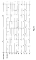
- FIG. 2 A timing chart during the digital drive of the EL display of the present invention is shown in Fig. 2.
- one frame period (F) is divided into n subframe periods (SF1 to SFn). Note that the period in which all of the pixels of the pixel portion display one image is referred to as one frame period (F).
- a normal EL display 60 or more frame periods are formed during one second, and 60 or more images are displayed during one second. If the number of images displayed during one second becomes fewer than 60, then problems such as image flicker start to become visually conspicuous.
- subframe periods a plurality of periods into which one frame period is additionally divided are referred to as subframe periods.
- the number of gradations increases, the number of frame period partitions increases, and the driver circuit must be driven at a high frequency.
- the subframe periods are divided into address periods (Ta) and sustain periods (Ts).
- the address period is the time required for inputting digital data signals into all of the pixels during one subframe period
- the sustain period also referred to as a turn on period denotes a period in which the EL element is made to emit light.
- the address periods (Ta) of SF1 to SFn become Ta1 to Tan, respectively.
- the sustain periods (Ts) of SF1 to SFn become Ts1 to Tsn, respectively.
- the opposite electrode of the EL elements 1506 is held at the steady-state potential of the same height as the power source electric potential.
- the steady-state potential in the address period of the digital driver is referred to as an off steady-state potential.
- the height of the off steady-state potential may be the same as the height of the power source electric potential within the range in which the EL elements 1506 do not emit light.
- the EL driver voltage at this time is referred to as the off EL driver voltage.
- the off EL driver voltage is 0V, but the voltage may be on the level on which the EL elements 1506 do not emit light.
- the gate signal is input to the gate signal line G1, and all the switching TFTs 1501 connected to the gate signal line G1 are turned on.
- a digital data signal is input into all of the source signal lines (S1 to Sx) at the same time.
- the digital data signal contains "0" or "1” information, and one of the digital data signals "0" and “1” has Hi electric voltage, while the other has Lo voltage.
- the digital data signal input into the source signal lines (S1 to Sx) is then input to the gate electrodes of the EL driver TFTs 1504 through the switching TFTs 1501, which are in the On state. Further, the digital data signal is also input to the capacitors 1508 of all of the pixels connected to the gate signal line G1, and an electric charge is stored.
- the gate signal is input to the gate signal line G2, and all of the switching TFTs 1501 connected to the gate signal line G2 are placed in the On state.
- the digital data signal is input to all of the source signal lines (S1 to Sx) at the same time.
- the digital data signal input to the source signal lines (S1 to Sx) is input to the gate electrodes of the EL driver TFTs 1504 through the switching TFTs 1501. Further, the digital data signal is also input to the capacitors 1508 of all of the pixels connected to the gate signal line G2, and stored.
- the digital data signal is input to all of the pixels.
- the period up until the digital data signal is input to all of the pixels is the address period.
- the sustain period commences at the same time as the address period is complete.
- the steady-state electric potential in the sustain period of the digital drive is referred to as the on steady-state electric potential in the embodiment mode of the present invention.
- the on steady-state electric potential may have an electric potential difference with the power source electric potential to the extent that the EL elements emit light. Note that this electric potential difference is referred to as an on EL driver voltage.
- the off steady-state electric potential and the on steady-state electric potential are generically referred to as steady-state electric potentials.
- the on EL driver voltage and an off EL driver voltage are generically referred to as EL driver voltages.
- All of the switching TFTs 1501 are set into the Off state in the sustain period.
- the digital data signal stored in the capacitors 1508 is then input to the gate electrodes of the EL driver TFTs 1504.
- the EL driver TFTs 1504 are set into the Off state in the embodiment mode of the present invention.
- the pixel electrodes of the EL elements 1506 are therefore maintained at the off steady-state electric potential.
- the EL elements 1506 contained in pixels to which the digital data signal containing "0" information is applied do not emit light.
- the EL driver TFTs 1504 turn on in the embodiment mode of the present invention.
- the electric power source electric potential is therefore imparted to the pixel electrodes of the EL elements 1506.
- EL elements 1506 contained in pixels to which the digital data signal having "1" information emit light.
- the Ts(n-1) period turns on predetermined pixels here.
- Ts(n-2), Ts(n-3), ..., Ts1 are set, in order, as sustain periods, and predetermined pixels are turned on in the respective subframes.
- One frame period is complete after the n subframe periods are completed.
- the brightness of light emitted by the EL elements during at least one sustain period is set to be always lower than the brightness of light emitted by the EL elements in other sustain periods.
- a sustain period in which the brightness of light emitted is 1/m of that emitted in other sustain periods is taken as Tsp (where p is an arbitrary number greater than or equal to 1 and less than or equal to n)
- the length of the sustain periods other than the sustain period Tsp is expressed as 2 -(n-1) T, where T is a positive constant.
- the length of the sustain period Tsp is expressed as 2 -(p-1) T ⁇ m. Note that m is a positive number greater than 1.
- the length of the sustain period Tsp is set to be 2 -(p-1) T ⁇ m, and the predetermined gray scale display can therefore be obtained.
- the present invention even if the Id-Vg characteristics of the TFTs vary slightly, dispersion in the amount of current output when equal gate voltages are applied can be suppressed by the above structure. It therefore becomes possible to avoid the situation in which the amount of light emitted by EL elements of adjacent pixels differs greatly due to variations in the Id-Vg characteristics, even with the same voltage signal input.
- the amount of time in which light is emitted by the EL elements can be set to 2 -(p-1) T ⁇ m (where T is a positive constant) in the sustain period Tsp, in which the brightness of light emitted by the EL elements is 1/m of the brightness emitted during other sustain periods.
- T is a positive constant
- the number of bits n becomes larger, and even if the length of the sustain period expressed by 2 -(n-1) T becomes shorter, the brightness of light emitted by the EL elements is regulated to be 1/m that emitted in other sustain periods, the length of the sustain period is set to 2 -(p-1) T ⁇ m, and it becomes possible to extend it.
- the electric power source electric potential is always maintained constant, the electric potential of the opposite electrodes is changed by the address period and the sustain period, and the off EL driver voltage or the on EL driver voltage is applied to the EL layers.
- the present invention is not limited to this structure.
- the electric potential of the opposite electrodes may be always maintained constant, and by changing the power source electric potential by the address period and the sustain period, the off EL driver voltage or the on EL driver voltage maybe applied to the EL layers. In this case, regulation of the brightness of the EL elements is performed by controlling the power source electric potential.
- the off EL driver voltage is taken as zero and the EL elements are not made to emit light, but the off EL driver voltage may also be set to the same voltage as the on EL driver voltage and light may also be emitted during the address period.
- the power source electric potential and the steady-state electric potential are always maintained at fixed values.
- the device of the invention can also be driven with the interlace scanning.
- the structure of the present invention is explained using an example of an EL display which performs time partitioning gradation display of digital driving method.
- An example of a circuit structure of the present invention is shown in Fig. 4.
- the EL display device of Fig. 4A has a pixel portion 101, and a source signal side driver circuit 102 and a gate signal side driver circuit 103 arranged in the periphery of the pixel portion, which are all composed of TFTs formed on a substrate.
- the EL display device has one source signal side driver circuit and one gate signal side driver circuit in the embodiment 1 of the present invention, two source signal side driver circuits may also be used in the present invention. Furthermore, two gate signal side driver circuits may also be used.
- the source signal side driver circuit 102 fundamentally contains a shift register 102a, a latch (A) 102b and a latch (B) 102c. Further, clock pulses (CK) and start pulses (SP) are input to the shift register 102a, digital data signals are input to the latch (A) 102b, and latch signals are input to the latch (B) 102c.
- clock pulses (CK) and start pulses (SP) are input to the shift register 102a
- digital data signals are input to the latch (A) 102b
- latch signals are input to the latch (B) 102c.
- gate signal side driver circuit 103 have shift resister and buffer.
- a multiplexer can be provided in the output side of the buffer.
- the digital data signals input to the pixel portion are formed by a time partitioning gradation data signal generator circuit 114.
- This circuit along with converting a video signal which is an analog signal or a digital signal (a signal containing image information) into a digital data signal for performing time partitioning gradation, is a circuit which generates timing pulses or the like which are necessary for performing time partitioning gradation display.
- a means of partitioning one frame period into a plurality of sub-frame periods corresponding to n-bit gradations (where n is a real number equal to or greater than 2), a means of selecting an address period and a sustain period in the plurality of sub-frame periods, and a means of setting the sustain periods.
- the time partitioning gradation data signal generator circuit 114 may also be formed external to the EL display device of the present invention. In this case, it becomes a structure that the digital data signals formed there are input to the EL display device of the present invention.
- An electronic device (EL display device) with the EL display device of the present invention as a display thus contains the EL display device of the present invention and the time partitioning gradation data signal generator circuit as separate components.
- the EL display device of the present invention may also be implemented with a form such as using an IC chip for the time partitioning gradation data signal generator circuit 114. In this case, it becomes a structure that the digital data signals formed by the IC chip are input to the EL display device of the present invention.
- An electronic device with the EL display device of the present invention as a display thus contains the EL display device of the present invention in which the IC chip containing the time partitioning gradation data signal generator circuit is implemented.
- the time partitioning gradation data signal generator circuit 114 may also be formed of TFTs on the same substrate as the pixel portion 101, the source signal side driver circuit 102, and the gate signal side driver circuit 103. In this case, all processing can be performed on the substrate provided that the video signal containing image information is input to the EL display device. It can be of course to form the time partitioning gradation data signal generator circuit with TFTs having polysilicon films used in the present invention as active layers. Furthermore, in this case an electronic device having the EL display device of the present invention as a display has the time partitioning gradation data signal generator circuit incorporated within the EL display device itself, and it is possible to make the electronic device small.
- a plurality of pixels 104 are arranged in a matrix state in the pixel portion 101.
- An expanded diagram of the pixels 104 is shown in Fig. 4B.
- Reference numeral 105 denotes a switching TFT in Fig. 4B.
- a gate electrode of the switching TFT 105 is connected to a gate signal line 106 which inputs a gate signal.
- One of a drain region and a source region of the switching TFT 105 is connected to a source signal line 107 for inputting a digital data signal, and the other is each connected to a gate electrode of an EL driver TFT 108 and capacitor 113 which is possessed by each pixel.
- a source region of the EL driver TFT 108 is connected to an electric power supply line 111, and a drain region is connected to an EL element 110.
- An electric power supply line 111 is connected to the capacitor 113.
- the capacitor 113 is provided to keep the gate voltage of an EL driver TFT 108 when the switching TFT 105 is non-selected state (Off state).
- the EL element 110 is composed of an anode and a cathode, and an EL layer which is provided between an anode and a cathode.
- An anode as an opposing electrode is maintained a fixed electric potential when the cathode is connected to a source region or the drain region of the EL driver TFT 110, in other words, the cathode is a pixel electrode.
- an anode as an opposing electrode is maintained a fixed electric potential when the cathode is connected to a source region or the drain region of the EL driver TFT 110, in other words, the cathode is a pixel electrode.
- the electric power supply line 111 is maintain the power supply potential.
- a resistive body may also be formed between the drain region or the source region of the EL driver TFT 108 and the EL element 110. It becomes possible to control the amount of current supplied to the EL element from the EL driver TFT, and to prevent any influence resulting in dispersion of the characteristics of the EL driver TFT with forming the resistive body.
- the resistive body may be an element displaying a resistance sufficiently larger than the on resistance of the EL driver TFT 108, and therefore there are no limitations in its structure. Note that the on resistance is the value of the drain voltage of the TFT divided by the drain current flowing at that the time.
- the resistance value of the resistive body may be selected in a range of 1 k ⁇ to 50 M ⁇ (preferably between 10 k ⁇ and 10 M ⁇ , more preferably between 50 k ⁇ and 1 M ⁇ ).
- Use of a semiconductor layer having high resistance value as the resistive body is preferably because it is easy to form.
- Fig. 5 schematically showing the sectional structure of the EL display device of the present invention.
- reference numeral 11 is a substrate, and 12 is an insulating film that is a base (hereinafter, this film is designated as base film).
- base film For the substrate 11, use can be made of a light transmissible substrate, representatively, a glass substrate, a quartz substrate, a glass ceramic substrate, or a crystallization glass substrate. However, it must be resistible to the highest processing temperature in a manufacturing process.
- the base film 12 is effective especially in using a substrate that has a movable ion or a substrate that has conductivity, but it is not necessarily disposed on the quartz substrate.
- An insulating film that contains silicon can be used as the base film 12. It should be noted that, in this specification, "insulating film that contains silicon” signifies an insulating film in which oxygen or nitrogen is added to silicon at a predetermined ratio (SiOxNy: x and y are arbitrary integers), such as a silicon oxide film, a silicon nitride film or a silicon nitride oxide film.
- Reference numeral 201 is a switching TFT
- 202 is a EL driver TFT.
- a switching TFT is formed by an n-channel type TFT.
- An EL driver is formed by a p-channel TFT.
- the above structure is preferable. However, in the present invention, there is no need to limit the above structure. It is also possible to use both the n-channel type TFT and p-channel type TFT for a switching TFT or an EL driver TFT.
- the switching TFT 201 is made up of an active layer that includes a source region 13, a drain region 14, LDD regions 15a-15d, an isolation region 16, and channel formation regions 17a, 17b, a gate insulating film 18, gate electrodes 19a, 19b, a 1st interlayer insulating film 20, a source wiring line (a part of a source signal line) 21, and a drain wiring line 22.
- the gate insulating film 18 or the 1st interlayer insulating film 20 can be common to all TFTs on the substrate, or can be varied according to circuits or elements.
- the gate electrodes 19a, 19b are connected electrically, in other words, a so-called double gate structure is established.
- a so-called multi gate structure such as a triple gate structure, can be established, of course.
- the multi gate structure signifies a structure including an active layer that has two channel formation regions or more connected in series.
- the multi gate structure is very effective to decrease an OFF-state current, and if the OFF-state current of the switching TFT is decreased sufficiently, the capacity necessary for the capacitor which is connected to a gate electrode of an EL driver TFT 202 can be reduced. That is, since the possession area of the capacitor can be reduced, the multi gate structure is also effective to widen the effective luminescence area of the EL element.
- the LDD regions 15a-15d are disposed not to overlap with the gate electrodes 19a and 19b, with the gate insulating film 18 therebetween.
- the thus built structure is very effective to decrease the OFF-state current.
- the length (width) of the LDD regions 15a-15d is 0.5-3.5mm, representatively, 2.0-2.5mm.
- an offset region i.e., region formed with a semiconductor layer whose composition is the same as the channel formation region, and in which a gate voltage is not applied
- the isolation region 16 i.e., region whose concentration is the same and to which the same impurity element is added as the source region or the drain region
- the isolation region 16 is effective to decrease the OFF-state current.
- the EL driver TFT 202 is made up of an active layer that includes a source region 26, a drain region 27, and a channel formation region 29, a gate insulating film 18, a gate electrode 30, the 1st interlayer insulating film 20, a source wiring line 31, and a drain wiring line 32.
- the EL driver TFT 202 is a p-channel type TFT.
- the drain region 14 of the switching TFT is connected to the gate electrode 30 of the EL driver TFT 202.
- the gate electrode 30 of the EL driver TFT 202 is connected electrically to the drain region 14 of the switching TFT 201 through the drain wiring line 22(also called connection wiring line). While the gate electrode 30 is a single gate structure here, the multi gate structure is also applied.
- the source wiring line 31 of the EL driving TFT 202 is connected to the current-feed line (not shown).
- the EL driver TFT 202 is an element to control the amount of current supplied to the EL element, and a comparatively large amount of current can flow therethrough. Therefore, preferably, the channel-width (W) is designed to be greater than the channel-width of the switching TFT. Additionally, preferably, the channel-length (L) is designed to be long so that an excessive current does not flow through the current controlling TFT 202. A desirable value is 0.5-2mA (1-1.5mA preferably) per pixel.
- the film thickness of the active layer (specifically, the channel formation region) of the EL driver TFT 202 50-100nm preferably, and 60-80nm further preferably.
- CMOS circuit that is a base unit to form the driving circuit is shown in Fig. 5.
- a TFT that has a structure to decrease the hot carrier injection without reducing the operation speed to the utmost is used as the n-channel type TFT 204 of the CMOS circuit.
- the driving circuit described herein is the source signal side driving circuit and the gate signal side driving circuit. It is also possible to form other logic circuits (level shifter, A/D converter, signal division circuit, etc.), of course.
- the active layer of the n-channel type TFT 204 of the CMOS circuit includes a source region 35, a drain region 36, an LDD region 37, and a channel formation region 38.
- the LDD region 37 overlaps with the gate electrode 39, with the gate insulating film 18 therebetween.
- the reason for forming the LDD region 37 only on the drain region 36 side is not to reduce the operation speed. There is no need to worry about the OFF-state current value in the n-channel type TFT 204. Instead, the operation speed should be rated above it. Therefore, preferably, the LDD region 37 is completely laid on the gate electrode, thus reducing a resistance component as much as possible. That is, a so-called offset should be omitted.
- the active layer includes a source region 40, a drain region 41, and a channel formation region 42.
- the gate insulating film 18 and the gate electrode 43 are disposed thereon. It is also possible to dispose the LDD region as well as the n-channel type TFT 204 in order to take countermeasures against the hot carrier, of course.
- the n-channel type TFT 204 and the p-channel type TFT 205 are covered with the first interlayer insulating film 20, and the source wiring lines (a part of the source signal lines) 44, 45 are formed.
- the n-channel type TFT 204 and the drain region of the p-channel type TFT 205 are connected electrically by the drain wiring line 46.
- Reference numeral 47 is a first passivation film.
- the film thickness thereof is 10nm-1mm (200-500nm preferably).
- An insulating film including silicon (especially, a silicon nitride oxide film or a silicon nitride film is desirable) can be used as its material.
- the passivation film 47 serves to protect a formed TFT from alkali metal and water.
- the EL layer finally disposed above the TFT (especially the EL driver TFT) includes alkali metal such as sodium.
- the first passivation film 47 serves also as a protective layer by which the alkali metal (movable ions) is not allowed to enter the TFT side.
- Reference numeral 48 is a second interlayer insulating film, and serves as a flattening film to flatten level differences formed by the TFT.
- an organic resin film such as polyimide, polyamide, acrylic resin, or BCB (benzocyclobutene) is used as the second interlayer insulating film 48.
- These films have an advantage in that a good smooth plane can be easily formed, and the dielectric constant is low. It is preferable to entirely absorb the level difference caused by the TFT by means of the second interlayer insulating film 48 because the EL layer is very sensitive to ruggedness.
- the film thickness thereof is 0.5-5mm (1.5-2.5mm preferably).
- Reference numeral 49 is a pixel electrode (anode of the EL element) that is made of a transparent conductive film. After a contact hole (opening) is made in the second interlayer insulating film 48 and the first passivation film 47, the electrode is connected to the drain wiring line 32 of the EL driver TFT 202 through the opening.
- the pixel electrode 49 and the drain region 27 are arranged not to be connected directly, as in Fig. 5, the alkali metal of the EL layer can be prevented from entering the active layer via the pixel electrode.
- a third interlayer insulating film 50 whose thickness is 0.3-1mm is disposed on the pixel electrode 49.
- the film 50 is made of a silicon oxide film, a silicon nitride oxide film, or an organic resin film.
- the third interlayer insulating film 50 is provided with an opening on the pixel electrode 49 by etching, and the edge of the opening is etched to have a taper shape.
- the angle of the taper is 10-60° (30-50° preferably).
- An EL layer 51 is formed on the third interlayer insulating film 50.
- the EL layer 51 is used in the form of a single-layer structure or a layered structure.
- the layered structure is superior in luminous efficiency.
- a positive hole injection layer/a positive hole transporting layer/a luminescent layer/an electronic transporting layer are formed on the pixel electrode in this order.
- a structure may be used which has the order of positive hole transporting layer/luminescent layer/electronic transporting layer or the order of positive hole injection layer/positive hole transporting layer/luminescent layer/electronic transporting layer/electronic injection layer.
- any one of the known structures can be used, and fluorescent coloring matter, etc., can be doped to the EL layer.
- the EL display device mainly has four color display methods; method of forming three kinds of EL elements that correspond to R(red), G(green), and B(blue), respectively; method of combining an EL element of white luminescence and a color filter; method of combining an EL element of blue or blue-green luminescence and a fluorescent body (fluorescent color conversion layer :CCM); and method of stacking the EL elements that correspond to RGB while using a transparent electrode for a cathode (opposite electrode).
- Fig. 5 The structure of Fig. 5 is an example in which the method of forming three kinds of EL elements that correspond to RGB is used. Only one pixel is shown in Fig. 5. In fact, pixels, each having the same structure, are formed to correspond to each color of red, green, and blue, and thereby color display can be performed.
- the present invention can be performed regardless of the luminescence method, and can use all the four methods. However, since the speed of response of the fluorescent body is slower than that of the EL, and the problem of afterglow occurs, the method in which the fluorescent body is not used is preferable. Additionally, it can be said that a color filter that causes the fall of luminescence brightness should not be used if possible.
- a cathode 52 of the EL element is disposed on the EL layer 51.
- a material that includes magnesium (Mg), lithium (Li) or calcium (Ca) that is small in work function is used as the cathode 52.
- a MgAgAl electrode, a LiAl electrode, or LiFAl electrode can be used.
- the luminescence element formed by the pixel electrode (anode), the EL layer, and the cathode is called an EL element 206.
- a layered body comprised of the EL layer 51 and the cathode 52 it is necessary to form a layered body comprised of the EL layer 51 and the cathode 52 by each pixel individually.
- the EL layer 51 is quite weak to water, and a normal photolithography technique cannot be used. Therefore, it is preferable to use a physical mask material, such as metal mask, and selectively form it according to a vapor phase method, such as a vacuum deposition method, a sputtering method, or a plasma CVD method.
- Reference numeral 53 is a protective electrode. This is to protect the cathode 52 from outside water, etc., and, at the same time, connect the cathode 52 of each pixel.
- the protective electrode 53 it is preferable to use a low-resistance material including aluminum (Al), copper (Cu), or silver (Ag). A cooling effect to lower the heat of the EL layer can be expected from the protective electrode 53. It is also effective to continue to the protective electrode 53 without air exposure after the above mentioned cathode 52 are formed.
- Reference numeral 54 is a second passivation film, and, preferably, the film thickness thereof is 10nm-1mm (200-500nm preferably).
- a main purpose to dispose the second passivation film 54 is to protect the EL layer 51 from water. It is also effective to give it a cooling effect.
- the EL layer is weak to heat as mentioned above, and film formation should be performed at a low temperature (ranging from a room temperature to 120°C preferably). Therefore, it can be said that a desirable film formation method is the plasma CVD method, sputtering method, vacuum deposition method, ion plating method, or solution application method (spin court method).
- the present invention is not limited to the structure of the EL display device of Fig. 5, which is just one of the preferred embodiments.
- the digital time division gray scale display method of the present invention is explained below using Fig. 6.
- a case of performing 2 4 gray scale display in accordance with a 4 bit digital data signal is explained here.
- Gate signal lines (G1 to Gy) for inputting a gate signal are connected to gate electrodes of switching TFTs in each pixel. Further, one of a source region and a drain region of the switching TFT of each pixel is connected to source signal lines (also referred to as data signal lines) (S1 to Sx) for inputting digital signals, and the other is connected to the gate electrode of an EL driver TFT and to a capacitor, of each pixel. Note that this structure in Embodiment 2 has capacitors, but a structure not including capacitors may also be used. There are no limitations upon the present invention by the presence of, or lack of, capacitors.
- One of the source region and the drain region of the EL driver TFT is connected to electric power source supply lines (V1 to Vx), and the other is connected to EL elements.
- the electric potential of the power source supply lines (V1 to Vx) is referred to as an electric power source electric potential. Further, the electric power source supply lines (V1 to Vx) are connected to the capacitors of each pixel.
- the EL elements are each composed of an anode, a cathode, and an EL layer formed between the anode and the cathode.
- the cathodes become opposite electrodes.
- the cathodes become the opposite electrodes.
- the electric potential of the opposite electrodes is referred to as a steady-state electric potential within this specification.
- the electric potential difference between the steady-state electric potential of the opposite electrodes and the power source electric potential of the pixel electrodes is an EL driver voltage, and the EL driver voltage is applied to the EL layers.
- FIG. 6 A timing chart for the EL display digital drive of the present invention is shown in Fig. 6.
- one frame period (F) is divided into four subframe periods (SF1 to SF4). Note that a period in which all of the pixels of the pixel portion display one image is referred to as one frame period (F).
- the subframe periods are divided into address periods (Ta) and sustain periods (Ts).
- the address period is the time required for inputting digital data signals into all of the pixels during one subframe period
- the sustain period also referred to as a turn on period denotes a period in which the EL element is made to emit light.
- the address periods (Ta) of SF1 to SF4 become Ta1 to Ta4, respectively.
- the sustain periods (Ts) of SF1 to SF4 become Ts1 to Ts4, respectively.
- the opposite electrode is held at the steady-state potential of the same height as the power source electric potential.
- the steady-state potential in the address period of the digital driver is referred to as an off steady-state potential.
- the height of the off steady-state potential may be the same as the height of the power source electric potential within the range in which the EL elements do not emit light.
- the EL driver voltage at this time is referred to as the off EL driver voltage.
- the off EL driver voltage is 0V, but the voltage may be on the level on which the EL elements do not emit light.
- the gate signal is input to the gate signal line G1, and all the switching TFTs connected to the gate signal line G1 are turned on.
- a digital data signal is input into all of the source signal lines (S1 to Sx) at the same time.
- the digital data signal contains "0" or "1” information, and one of the digital data signals "0" and “1” has Hi electric voltage, while the other has Lo voltage.
- the digital data signal input into the source signal lines (S1 to Sx) is then input to the gate electrodes of the EL driver TFTs through the switching TFTs, which are in the On state. Further, the digital data signal is also input to the capacitors of all of the pixels connected to the gate signal line G1, and an electric charge is stored.
- the gate signal is input to the gate signal line G2, and all of the switching TFTs connected to the gate signal line G2 are placed in the On state.
- the digital data signal is input to all of the source signal lines (S1 to Sx) at the same time.
- the digital data signal input to the source signal lines (S1 to Sx) is input to the gate electrodes of the EL driver TFTs through the switching TFTs. Further, the digital data signal is also input to the capacitors of all of the pixels connected to the gate signal line G2, and stored.
- the digital data signal is input to all of the pixels.
- the period up until the digital data signal is input to all of the pixels is the address period.
- the sustain period commences at the same time as the address period is complete.
- the steady-state electric potential in the sustain period of the digital drive is referred to as the on steady-state electric potential in the embodiments of the present invention.
- the on steady-state electric potential may have an electric potential difference with the power source electric potential to the extent that the EL elements emit light. Note that this electric potential difference is referred to as an on EL driver voltage.
- the off steady-state electric potential and the on steady-state electric potential are generically referred to as steady-state electric potentials.
- the on EL driver voltage and an off EL driver voltage are generically referred to as EL driver voltages.
- All of the switching TFTs are set into the Off state in the sustain period.
- the digital data signal stored in the capacitors is then input to the gate electrodes of the EL driver TFTs.
- the EL driver TFTs are set into the Off state in the embodiments of the present invention.
- the pixel electrodes of the EL elements are therefore maintained at the off steady-state electric potential.
- the EL elements contained in pixels to which the digital data signal containing "0" information is applied do not emit light.
- the EL driver TFTs turn on in the embodiments of the present invention.
- the electric power source electric potential is therefore imparted to the pixel electrodes of the EL elements.
- EL elements contained in pixels to which the digital data signal having "1" information emit light.
- the Ts3 period turns on predetermined pixels here.
- Ts2 and Ts1 are set, in order, as sustain periods, and predetermined pixels are turned on in the respective subframes.
- One frame period is complete after the 4 subframe periods are completed.
- the brightness of light emitted by the EL elements during at least one sustain period is set to be always lower than the brightness of light emitted by the EL elements in other sustain periods.
- the brightness of light emitted by the EL elements during the sustain periods Ts3 and Ts4 is one-half the brightness of light emitted by the EL elements during the sustain periods Ts1 and Ts2.
- the on EL driver voltage during the sustain periods Ts3 and Ts4 is one-half the EL driver voltage during the other sustain periods Ts1 and Ts2.
- the length of the sustain periods Ts1 and Ts2, the sustain periods other than the sustain periods Ts3 and Ts4 having an emitted light brightness of one-half that of Ts1 and Ts2, is expressed as T and 2 -1 T, respectively, where T is a positive constant. Further, the length of the sustain periods Ts3 and T4 is expressed as 2 -2 T ⁇ 2 and 2 -3 T ⁇ 2, respectively. Namely, the ratio of lengths of the sustain periods Ts1 to Ts4 is 1 : 2 -1 : 2 -1 : 2 -2 .
- the ratio of lengths of the sustain periods Ts3 and Ts4 to all of the sustain periods is twice that of a case in which the brightness of light emitted is not set to one-half. Therefore, even though the brightness of light emitted by the EL elements in the sustain periods Ts3 and Ts4 is one half that of the other sustain periods, the length ratio of the sustain periods Ts3 and Ts4 is set to twice as long, and the desired gray scale display can be obtained.
- the present invention even if the Id-Vg characteristics of the TFTs vary slightly, dispersion in the amount of current output when equal gate voltages are applied can be suppressed by the above structure. It therefore becomes possible to avoid the situation in which the amount of light emitted by EL elements of adjacent pixels differs greatly due to variations in the Id-Vg characteristics, even with the same video signal input.
- a sustain period Tsp in which the brightness of light emitted is 1/m of that emitted in other sustain periods Ts1 to Tsn if the length of the other sustain periods Ts1 to Tsn is taken as 2 -(n-1) T, where T is a positive constant, then the amount of time in which light is emitted by the EL elements can be taken as 2 -(p-1) T ⁇ m.
- the length ratio of the sustain period Tsp to all of the sustain periods can be extended by a multiple of m compared to a case in which the brightness of light emitted during the sustain period Tsp is not set to 1/m. Therefore, in accordance with increasing the number of image gradations, even if the number of bits n becomes larger and the length of the sustain periods becomes shorter, the length of the sustain periods can be extended by lowering the brightness of the light emitted by the EL elements.
- Embodiment 2 an example of driving by non-interlaced scanning is explained in Embodiment 2, but it is also possible to drive by interlacing.
- Embodiment 2 Note that it is possible to freely combine Embodiment 2 with Embodiment 1.
- CMOS circuit that is a base unit is shown in the figure, for a brief description.
- a substrate 501 in which a base film (not shown) is disposed on the surface thereof is prepared as shown in Fig. 7(A).
- a silicon nitride oxide film whose thickness is 200nm and another silicon nitride oxide film whose thickness is 100nm are laminated and are used as a base film on a crystallization glass.
- the concentration of nitrogen of the film contacting the crystallization glass substrate is kept to 10-25wt%. It is possible to form an element directly on the quartz substrate without any base film, of course.
- an amorphous silicon film 502 whose thickness is 45nm is formed on the substrate 501 by a well-known film formation method. There is no need to limit it to the amorphous silicon film. Instead, a semiconductor film (including a microcrystal semiconductor film) that has an amorphous structure can be used in this embodiment. A compound semiconductor film that has an amorphous structure, such as an amorphous silicon germanium film, also can be used herein.
- a protective film 504 that has openings 503a and 503b is formed.
- a silicon oxide film 150nm thick is used in this embodiment.
- a layer 505 (Ni containing layer) that contains nickel (Ni) is formed on the protective film 504 by a spin court method. Concerning the formation of the Ni containing layer, reference can be made to the above publication.
- amorphous silicon film 502 is crystallized.
- crystallization progresses substantially in parallel with the substrate, starting from regions 506a and 506b (hereinafter, designated as Ni addition region) with which Ni is in contact.
- Ni addition region regions 506a and 506b (hereinafter, designated as Ni addition region) with which Ni is in contact.
- a polysilicon film 507 is formed that has a crystal structure in which bar crystals gather and form lines.
- an element (phosphorus preferably) that belongs to 15-family is added to the Ni addition regions 506a and 506b, while leaving the protective film 504 as a mask.
- Regions 508a and 508b (hereinafter, designated as phosphorus addition region) to which phosphorus was added at high concentration are thus formed.
- the concentration of Ni remaining in the polysilicon film 509 is reduced to at least 2 x 10 17 atoms/cm 3 according to the measurement value by SIMS (mass secondary ion analysis).
- SIMS mass secondary ion analysis
- the polysilicon film 509 can be thus obtained that is crystallized by a catalyst and is decreased to the level in which the catalyst does not obstruct the operation of a TFT. Thereafter, active layers 510-513 that use the polysilicon film 509 only are formed by a patterning process. At this time, a marker to conduct mask alignment in the following patterning should be formed by using the above polysilicon film. (Fig. 7(D))
- a silicon nitride oxide film 50nm thick is formed by the plasma CVD method as shown in Fig. 7(E), heating processing at 950°C for 1 hour is then performed in an oxidation atmosphere, and a thermal oxidation process is performed.
- the oxidation atmosphere can be an oxygen atmosphere or another oxygen atmosphere in which halogen is added.
- the oxidation progresses in the interface between the active layer and the silicon nitride oxide film, and a polysilicon film whose thickness is about 15nm is oxidized, so that a silicon oxide film whose thickness is about 30nm is formed. That is, a gate insulating film 514 of a thickness of 80nm is formed in which the silicon oxide film 30nm thick and the silicon nitride oxide film 50nm thick are laminated.
- the film thickness of the active layers 510-513 is made 30nm by the thermal oxidation process.
- a resist mask 515 is formed, and an impurity element (hereinafter, designated as p-type impurity element) that gives the p-type through the medium of the gate insulating film 514 is added.
- p-type impurity element an element that belongs to 13-family representatively, boron or gallium typically, can be used. This (called a channel dope process) is a process for controlling the threshold voltage of a TFT.
- boron is added by the ion dope method in which plasma excitation is performed without the mass separation of diborane (B 2 H 6 ).
- the ion implantation method that performs the mass separation can be used, of course.
- impurity regions 516-518 are formed that include boron at the concentration of 1 x 10 15 -1 x 10 18 atoms/cm 3 (5 x 10 16 -5 x 10 17 atoms/cm 3 representatively).
- n-type impurity element an impurity element that gives the n-type through the medium of the gate insulating film 514 is added.
- n-type impurity element an element that belongs to 15-family representatively, phosphorus or arsenic typically, can be used.
- a plasma doping method in which plasma excitation is performed without the mass separation of phosphine (PH 3 ) is used. Phosphorus is added in the concentration of 1 x 10 18 atoms/cm 3 .
- the ion implantation method that performs mass separation can be used, of course.
- a dose amount is adjusted so that the n-type impurity element is included in the n-type impurity regions 520, 521 formed by this process at the concentration of 2 x 10 16 -5 x 10 19 atoms/cm 3 (5 x 10 17 -5 x 10 18 atoms/cm 3 representatively).
- a process is performed for activating the added n-type impurity element and the added p-type impurity element as shown in Fig. 8(C).
- the activation means since the gate insulating film 514 is disposed, the furnace annealing process that uses an electro-thermal furnace is desirable. Additionally, it is preferable to perform heat processing at a temperature as high as possible because there is a possibility of having damaged the interface between the active layer and the gate insulating film of a part that is a channel formation region in the process of Fig. 8(A).
- the activating process is performed by the furnace annealing processing at 800°C for 1 hour.
- the thermal oxidation can be performed keeping a processing atmosphere in an oxidizing atmosphere, or the heat processing can be performed in an inert atmosphere.
- This process clarifies the edge of the n-type impurity regions 520, 521, namely, the boundary (junction) between the n-type impurity regions 520,521 and the region (p-type impurity region formed by the process of Fig. 8(A)) around the n-type impurity regions 520, 521, where the n-type impurity element is not added.
- each TFT channel is decided by the line width of those gate electrodes 522-525.
- the gate electrode can be made of a conductive film of a single-layer, however, preferably, a lamination film, such as two-layer or three-layer film, is used when necessary.
- a known conductive film can be used as the material of the gate electrode.
- use can be made of a film of an element selected from the group consisting of aluminum (Al), tantalum (Ta), titanium (Ti), molybdenum (Mo), tungsten (W), chrome (Cr), and silicon (Si) having conductivity; a film of a nitride of the aforementioned elements (tantalum nitride film, tungsten nitride film, or titanium nitride film representatively); an alloy film of a combination of the aforementioned elements (Mo-W alloy or Mo-Ta alloy representatively); or, a suicide film of the aforementioned elements (tungsten suicide film or titanium suicide film representatively). They can have a single-layer structure or a lamination-layer structure, of course.
- a lamination film is used that is made of a tungsten nitride (WN) film 50nm thick and a tungsten (W) film 350nm thick. This can be formed by the sputtering method. By adding an inert gas, such as Xe or Ne, as a spattering gas, the film can be prevented from peeling off because of stress.
- WN tungsten nitride
- W tungsten
- the gate electrodes 523, 525 are formed to overlap with part of the n-type impurity regions 520, 521, respectively, with the gate insulating film 514 therebetween.
- the overlapping part is later made an LDD region overlapping with the gate electrode.
- the gate electrodes 524a and 524b are seen as separate, in fact, they are connected electrically to each other.
- an n-type impurity element (phosphorus in this embodiment) is added self-adjustably, as shown in Fig. 9(A).
- an adjustment is performed so that phosphorus is added to the thus formed impurity regions 527-533 at the concentration of 2/1-1/10 (1/3-1/4 representatively) of that of the n-type impurity regions 520, 521.
- the concentration is 1 x 10 16 -5 x 10 18 atoms/cm 3 (3 x 10 17 -3 x 10 18 atoms/cm 3 typically).
- resist masks 534a-534d are formed to cover the gate electrode, an n-type impurity element (phosphorus in this embodiment) is then added, and impurity regions 535-541 including a high concentration of phosphorus are formed.
- the ion dope method using phosphine (PH 3 ) is applied also herein, and an adjustment is performed so that the concentration of phosphorus in these regions is 1 x 10 20 -1 x 10 21 atoms/cm 3 (2 x 10 20 -5 x 10 21 atoms/cm 3 representatively).
- a source region or a drain region of the n-channel type TFT is formed through this process, and the switching TFT leaves a part of the n-type impurity regions 530-532 formed in the process of Fig. 9(A).
- a resist mask 543 is newly formed.
- a p-type impurity element (boron in this embodiment) is then added, and impurity regions 544, 545 including a high concentration of boron are formed.
- boron is added to obtain a concentration of 3 x 10 20 -3 x 10 21 atoms/cm 3 (5 x 10 20 -1 x 10 21 atoms/cm 3 representatively).
- Phosphorus has been already added to the impurity regions 544, 545 at a concentration of 1 x 10 20 -1 x 10 21 atoms/cm 3 . Boron added herein has at least three times as high concentration as the added phosphorus. Therefore, the impurity region of the n-type formed beforehand is completely changed into that of the p-type, and functions as an impurity region of the p-type.
- a first interlayer insulating film 546 is formed.
- an insulating film that includes silicon is used in the form of a single-layer structure or a stacked-layer structure as a combination thereof.
- the film thickness thereof is 400nm-1.5 ⁇ m.
- a structure is created in which an 800nm-thick silicon oxide film is stacked on a 200nm-thick silicon nitride oxide film.
- the furnace annealing method is desirable as an activation means.
- heat treatment is performed at 550°C for 4 hours in a nitrogen atmosphere in an electro-thermal furnace.
- Heat treatment is further performed at 300-450°C for 1-12 hours in an atmosphere that includes hydrogen of 3-100% for hydrogenation. This is a process to hydrogen-terminate an unpaired connector of a semiconductor film by thermally excited hydrogen.
- plasma hydrogenation hydrogen excited by plasma is used
- Hydrogenation can be performed during the formation of the first interlayer insulating film 546.
- the 200nm-thick silicon nitride oxide film is formed, and hydrogenation is performed as mentioned above, and thereafter the remaining 800nm-thick silicon oxide film can be formed.
- this electrode is formed with a lamination film of a three-layer structure in which a 100nm-thick Ti film, a 300nm-thick aluminum film that includes Ti, and a 150nm-thick Ti film are continuously formed according to the sputtering method.
- Other conductive films can be used, of course.
- a first passivation film 554 is formed to be 50-500nm thick (200-300nm thick representatively).
- a 300nm-thick silicon nitride oxide film is used as the first passivation film 554.
- a silicon nitride film can be substituted for this.
- a second interlayer insulating film 555 made of organic resin is formed.
- Polyimide, acrylic fiber, or BCB (benzocyclobutene) can be used as the organic resin.
- an acrylic film excellent in smoothness is desirable.
- An acrylic film is formed to be 2.5 ⁇ m thick in this embodiment.
- a protective electrode 556 is formed.
- a conductive film largely composed of aluminum can be used as the protective electrode 556.
- the protective electrode 556 can be formed according to the vacuum deposition method.
- an insulating film (a silicon oxide film in this embodiment) that includes silicon is formed to be 500nm thick, an opening is then formed at the position corresponding to the pixel electrode, and a third interlayer insulating film 557 is formed. It is possible to easily form a tapered sidewall by using the wet etching method when the opening is formed. If the sidewall of the opening does not have a sufficiently gentle slope, deterioration of the EL layer caused by level differences will lead to an important problem.
- a opposite electrode (MgAg electrode) 558 which is a cathode of an EL element is formed.
- the MgAg electrode 558 is formed using the vacuum deposition method to make the film thickness 180-300nm (200-250nm typically).
- an EL layer 559 is formed without air exposure by the vacuum deposition method.
- the film thickness of the EL layer 559 is 800-200nm (100-120 nm typically) and the pixel electrode (anode) 560 thereof is 110 nm.
- an EL layer and a pixel electrode are sequentially formed for a pixel corresponding to red, a pixel corresponding to green, and a pixel corresponding to blue.
- the EL layer is poor in tolerance to solutions, they must be independently formed for each color without using the photolithography technique.
- a mask is first set for concealing all pixels except a pixel corresponding to red, and an EL layer and a pixel electrode (anode) of red luminescence are selectively formed by the mask. Thereafter, a mask is set for concealing all pixels except a pixel corresponding to green, and an EL layer and a pixel electrode (anode) of green luminescence are selectively formed by the mask. Thereafter, as above, a mask is set for concealing all pixels except a pixel corresponding to blue, and an EL layer and a pixel electrode (anode) of blue luminescence are selectively formed by the mask. In this case, the different masks are used for the respective colors. Instead, the same mask may be used for them. Preferably, processing is performed without breaking the vacuum until the EL layer are formed for all the pixels.
- a known material can be used for the EL layer 559.
- the EL layer can be formed with a four-layer structure consisting of a positive hole injection layer, a positive hole transporting layer, a luminescent layer, and an electronic injection layer.
- indium tin oxide film is formed as a pixel electrode (anode) of an EL layer.
- a transparent conductive film can be used in which zinc oxide (ZnO) of 2-20% is mixed with indium oxide or other well-known materials also can be used.
- a second passivation film 561 made of a silicon nitride film is formed to be 300nm thick.
- an EL display device constructed as shown in Fig. 10(C) is completed.
- the device is packaged (sealed) by a highly airtight protective film (laminate film, ultraviolet cured resin film, etc.) or a housing material such as a ceramic sealing can, in order not to be exposed to the air when completed as shown in Fig. 10(C).
- a highly airtight protective film laminate film, ultraviolet cured resin film, etc.
- a housing material such as a ceramic sealing can, in order not to be exposed to the air when completed as shown in Fig. 10(C).
- the reliability (life) of the EL layer is improved by making the inside of the housing material an inert atmosphere or by placing a hygroscopic material (for example, barium oxide) therein.
- a hygroscopic material for example, barium oxide
- the present embodiment can be freely combined with an embodiment 2.
- the EL display device of this embodiment is made up of a pixel portion 2202, a gate signal side driving circuit 2203, and a source side driving circuit 2204, each formed on a glass substrate 2201.
- a switching TFT 2205 of the pixel portion 2202 is an n-channel type TFT, and is disposed at the intersection of a gate wiring line 2206 connected to the gate side driving circuit 2203 and a source wiring line 2207 connected to the source side driving circuit 2204.
- the drain region of the switching TFT 2205 is connected to the gate electrode of the EL driver TFT 2208.
- the source region of the EL driver TFT 2208 is connected to a current-feed line 2209.
- a capacitor 2216 is provided, which is connected to the gate electrode and the current-feed line 2209 of the EL driver TFT 2208.
- electric supply potential is added to the current-feed line 2209. Further, a common potential is added to the opposite electrode (cathode in this embodiment) of the EL element 2211.
- a FPC 2212 which is an external input-output terminal is provided with input wiring lines (connection wiring lines) 2213, 2214 for transmitting a signal to the driving circuit, and an input-output wiring line 2214 connected to the current-feed line 2209.
- EL module of this embodiment including housing materials will now be described with reference to Figs. 12(A) and 12(B). Reference characters used in Fig. 11 are again used when necessary.
- a pixel portion 2202, a gate signal side driving circuit 2203, and a source signal side driving circuit 2204 are formed on a glass substrate 2201.
- Various wiring lines from each driving circuit are connected to external equipment via the input-output wiring lines 2213 to 2215 and the FPC 2212.
- a substrate 2304 is disposed so as to overlap at least the pixel portion 2202, preferably the pixel portion 2202 and the driving circuit 2203, 2204.
- the protective substrate 2304 is fixed to the glass substrate 2201 by a seal material 2305 so as to form closed space in cooperation with the glass substrate 2201.
- the EL element is in a state of being completely enclosed in the closed space, and is completely intercepted from the outside air.
- the closed space which is formed by a glass substrate 2201, a protective substrate 2304 and a seal material 2305 is called a cell 2306.
- the plurality of cell 2306 can be formed by disposing a plurality of protective substrate 2304.
- the quality of the protective substrate 2304 is an insulating substance such as glass or polymer.
- insulating substance such as glass or polymer.
- amorphous glass borosilicate glass, quartz, etc.
- crystallization glass ceramics glass
- ceramics glass organic resin (acrylic resin, styrene resin, polycarbonate resin, epoxy resin, etc.) or silicone resin.
- ceramics can be used.
- metallic materials such as stainless alloy, if the seal material 2305 is an insulating material.
- epoxy resin epoxy resin, acrylate resin, etc.
- thermosetting resin or light curing resin can be used as the adhesive.
- it is required to be a material that does not transmit oxygen and water to the utmost.
- PVC poly vinyl chloride
- epoxy resin silicon resin
- PVB poly vinyl butyral
- EVA ethylene vinyl acetate
- acrylic and polyimide etc. can be used.
- a dryer described in Japanese Laid-open Patent Publication Hei 9-148066 can be used as the drying agent.
- barium oxide can be used.
- the pixel portion is provided with a plurality of pixels, each having individually isolated EL elements. All of them have a protective electrode 2307 as a common electrode.
- a description was given as follows: it is preferable to continuously form the EL layer, the cathode (MgAg electrode), and the protective electrode without air exposure. Instead, if the EL layer and the cathode are formed by using the same mask material, and only the protective electrode is formed by another mask, a structure of Fig. 12(B) will be realized.
- the EL layer and the cathode can be disposed on the pixel portion only, and are not required to be disposed on the driving circuit. No problem will occur even if they are disposed on the driving circuit, of course. However, they should not be disposed thereon in consideration of the fact that an alkali metal is included in the EL layer.
- the protective electrode 2307 is connected to an input-output wiring line 2310 in the region shown by reference numeral 2308 through the medium of a connection wiring line 2309 that is made of the same material as the pixel electrode.
- the input-output wiring line 2310 is a current-feed line to give a EL driving potential to the protective electrode 2307, and is connected to the FPC 2212 through the medium of a conductive paste material 2311.
- Embodiment 5 there will be explained a structure of a pixel of an EL display according to the present invention.
- a plurality of pixels are arranged in matrix.
- Fig. 13A shows an example of a circuit diagram of the pixel.
- a switching TFT 1001 is provided in Fig. 13A.
- a switching TFT 1001 either an n-channel TFT or a p-channel TFT may be used.
- the n-channel TFT is used as the switching TFT 1001.
- the gate electrode of the switching TFT 1001 is connected to the gate signal line 1002 for inputting a gate signal.
- One of the source region and the drain region of the switching TFT 1001 is connected to the data signal line (also referred to as source signal line) 1003 for inputting a digital data signal while the other is connected to the gate electrode of the EL driver TFT 1004.
- One of the source region and the drain region of the EL driver TFT 1004 is connected to the power source supply line 1005 while the other is connected to the EL element 1006.
- the EL element 1006 comprises an anode, a cathode and an EL layer provided between the anode and the cathode.
- the anode is a pixel electrode and the cathode is an opposite electrode
- either the source region or the drain region of the EL driver TFT 1004 is connected to the anode of the EL element 1006.
- the cathode is the pixel electrode
- either the source region or the drain region of the EL driver TFT is connected to the cathode of the EL element 1006.
- the EL driver TFT 1004 either n-channel TFT or p-channel TFT may be used. However, in the case where the anode of the EL element 1006 is the pixel electrode and the cathode is the opposite electrode, it is preferable that the EL driver TFT 1004 is the p-channel TFT. Furthermore, on the contrary, in the case where the anode of the EL element 1006 is the opposite electrode, and the cathode is the pixel electrode, it is preferable that the EL driver TFT 1004 is an n-channel TFT. In Fig. 13A, the p-channel TFT is used as the EL driver TFT 1004. The cathode of the EL element 1006 is connected to the steady-state power source 1007.
- a capacitor may be provided to hold the gate voltage of the EL driver TFT 1004.
- the capacitor is connected between the one of the source region and the drain region of the switching TFT 1001 which is not connected to the source signal line, and the power source supply line 1005.
- the power source supply line 1005 is arranged in parallel with the source signal line 1003.
- an LDD region may be formed within the active layer of the EL driver TFT 1004, and a region may be formed (Lov region) in which the LDD region and the gate electrode overlap through the gate insulating film.
- a capacitance can be formed between the gate electrode of the EL driver TFT 1004 and the Lov region, and the gate voltage of the EL driver TFT 1004 can be stored, whether the EL driver TFT 1004 is an n-channel TFT or a p-channel TFT.
- the on current can be increased by forming the Lov region in the drain region side of the active layer.
- the Lov region of the EL driver TFT as a capacitor for storing the gate voltage of the EL driver TFT 1004
- a capacity value of about 19.8fF is required in the case where the pixel size is 22 ⁇ m ⁇ 22 ⁇ m, the thickness of the gate insulating film is 800 ⁇ and the relative dielectric constant of the gate insulating film is 4.1. Consequently, as the area of the Lov region (an area in which the LDD region and the gate electrode are overlapped via the gate insulating film), an area of about 66 ⁇ m 2 is required.
- either the switching TFT 001 or the EL driver TFT 1004 may be formed into a multi-gate structure (a structure including an active layer having two or more channel forming regions connected in series).
- Fig. 14A shows a circuit diagram of a pixel in which the switching TFT 1001 of the pixel shown in Fig. 13A is formed into a multi-gate structure.
- the switching TFT 1001a and the switching TFT 1001b are formed connected in series. Except for the switching TFTs 1001a and 1001b, the structure is the same as the circuit diagram shown in Fig. 13A.
- the switching TFTs multi-gate structures By making the switching TFTs multi-gate structures, the off current can be lowered, and the gate voltage of the EL driver TFT 1004 can be stored without forming a capacitor, in particular. Therefore, a capacitor for storing the gate voltage of the EL driver TFT 1004 need not be formed.
- a double gate structure is used in Fig. 14A, but the present invention is not limited to a double gate structure, and any multi-gate structure may be used.
- the deterioration of the EL driver TFT by heat can be suppressed.
- Fig. 13B shows another example of the circuit diagram of the pixel according to the present invention.
- the switching TFT 1101 is provided in the pixel 1100.
- the n-channel TFT or the p-channel TFT may be used as the switching TFT 1101.
- the n-channel TFT is used as the switching TFT 1101.
- the gate electrode of the switching TFT 1101 is connected to the gate signal line 1102 for inputting the gate signal.
- One of the source region and the drain region of the switching TFT 1101 is connected to the data signal line (also referred to as a source signal line) 1103 for inputting a digital data signal while the other is connected to the gate electrode of the EL driver TFT 1104.
- one of the source region and the drain region of the EL driver TFT 1104 is connected to the power source supply line 1105 while the other is connected to the EL element 1106.
- the EL element 1106 comprises an anode, a cathode and an EL layer provided between the anode and the cathode.
- the anode is the pixel electrode and the cathode is the opposite electrode
- either the source region or the drain region of the EL driver TFT 1104 is connected to the anode of the EL element 1106.
- the anode is the opposite electrode and the cathode is the pixel electrode
- either the source region or the drain region of the EL driver TFT 1104 is connected to the cathode of the EL element 1106.
- the EL driver TFT 1104 either the n-channel TFT or the p-channel TFT may be used.
- the EL driver TFT 1104 is the p-channel TFT. Furthermore, on the contrary, in the case where the anode of the EL element 1106 is the opposite electrode and the cathode thereof is the pixel electrode, it is preferable that the EL driver TFT 1104 is the n-channel TFT. In Fig. 13B, the p-channel TFT is used in the EL driver TFT 1104. The cathode of the EL element 1106 is connected to the steady-state power source 1107.
- a capacitor may be provided to hold the gate voltage of the EL driver TFT 1104.
- the capacitor is connected between the one of the source region and the drain region of the switching TFT 1101 which is not connected to the source signal line, and the power source supply line 1105.
- the power source supply line 1105 and the gate signal line 1102 are arranged in parallel.
- an LDD region may be formed within the active layer of the EL driver TFT 1104, and a region may be formed (Lov region) in which the LDD region and the gate electrode overlap through the gate insulating film.
- a capacitance can be formed between the gate electrode of the EL driver TFT 1004 and the Lov region, and the gate voltage of the EL driver TFT 1004 can be stored, whether the EL driver TFT 1104 is an n-channel TFT or a p-channel TFT.
- the on current can be increased by forming the Lov region in the drain region side of the active layer.
- Fig. 14B shows a circuit diagram of a pixel in which the switching TFT 1101 of the pixel shown in Fig. 13B is formed into a multi-gate structure.
- the switching TFT 1101a and the switching TFT 1101b are formed connected in series. Except for the switching TFTs 1101a and 1101b, the structure is the same as the circuit diagram shown in Fig. 13B.
- the switching TFTs multi-gate structures By making the switching TFTs multi-gate structures, the off current can be lowered, and the gate voltage of the EL driver TFT 1104 can be stored without forming a capacitor, in particular. Therefore, a capacitor for storing the gate voltage of the EL driver TFT 1104 need not be formed.
- a double gate structure is used in Fig. 14B, but the present invention is not limited to a double gate structure, and any multi-gate structure may be used.
- the deterioration of the EL driver TFT by heat can be suppressed.
- Fig. 15A shows another example of a circuit diagram of a pixel according to the present invention.
- the pixel 1200 and the pixel 1210 are provided adjacent to each other.
- reference numerals 1201 and 1211 denote switching TFTs. Note that, in the present invention, as switching TFTs 1201 and 1211, either the n-channel TFT or the p-channel TFT may be used.
- the n-channel TFT is used in the switching TFT 1201 and the switching TFT 1211.
- the gate electrodes of the switching TFTs 1201 and 1211 are connected to the gate signal line 1202 for inputting the gate signal.
- One of the source region and the drain region of the switching TFTs 1201 and 1211 is connected to the data signal lines 1203 and 1204 (hereinafter referred to as a source signal line) for inputting a digital data signal while the other is connected to the gate electrodes of the EL driver TFTs 1204 and 1214, respectively.
- one of the source region and the drain region of the EL driver TFTs 1204 and 1214 is connected to the power source supply line 1220 while the other is connected to the EL elements 1205 and 1215, respectively.
- two adjacent pixels share one power source supply line 1220.
- the number of the power source supply lines can be decreased.
- the ratio of the wiring with respect to the whole pixel portion is small, the light shielding by the wiring can be suppressed in the case where the wiring is provided in a direction of the light emission of the EL layer.
- the EL elements 1205 and 1215 comprise an anode, a cathode, and an EL layer provided between the anode and the cathode respectively.
- the anode is the pixel electrode and the cathode is the opposite electrode
- either the source region or the drain region of the EL driver TFTs 1204 and the 1214 is connected to the anodes of the EL elements 1205 and 1215.
- the cathode is the pixel electrode
- either the source region or the drain region of the EL driver TFTs 1204 and 1214 is connected to the cathodes of the EL elements 1205 and 1215.
- the EL driver TFTs 1204 and 1214 either the n-channel TFT or the p-channel TFT may be used.
- the EL driver TFTs 1204 and 1214 are the p-channel TFTs.
- the EL driver TFTs 1204 and 1214 are n-channel TFTs.
- the EL driver TFTs 1204 and 1214 are n-channel TFTs.
- the EL driver TFTs 1204 and 1214 are used as the EL driver TFTs 1204 and 1214.
- the cathodes of the EL elements 1205 and 1215 are connected to the steady-state power sources 1206 and 1216.
- a capacitor may be provided for storing the gate voltage of the EL driver TFTs 1204 and 1214.
- the capacitor may be connected between the one of the drain region and the source region of the swithing TFT 1201 which is not connected to the source signal line and the power source supply line 1220.
- an LDD region may be formed within the active layer of the EL driver TFTs 1204 and 1214, and a region may be formed (Lov region) in which the LDD region and the gate electrode overlap through the gate insulating film.
- a capacitance can be formed between the gate electrodes of the EL driver TFTs 1204 and 1214 and the Lov region, and the gate voltages of the EL driver TFT 1204 and 1214 can be stored, whether the EL driver TFT 1204 is an n-channel TFT or a p-channel TFT.
- the on current can be increased by forming the Lov region in the drain region side of the active layer.
- the switching TFT 1201 and 1211, or the EL driver TFTs 1204 and 1214 may be formed into a multi-gate structure.
- Fig. 16A shows a circuit diagram of a pixel in which the switching TFTs 1201 and 1211 are formed into the multi-gate structure of a pixel shown in Fig. 15A.
- the switching TFT 1201a and the switching TFT 1201b are formed connected in series.
- the switching TFT 1211a and the switching TFT 1211b are also formed connected in series. Except for the switching TFTs 1201a and 1201b and the switching TFTs 1211a and 1211b, the structure is the same as the circuit diagram shown in Fig. 15A.
- the switching TFTs multi-gate structures By making the switching TFTs multi-gate structures, the off current can be lowered, and the gate voltage of the EL driver TFTs 1204 and 1214 can be stored without forming a capacitor, in particular. Therefore, a capacitor for storing the gate voltages of the EL driver TFTs 1204 and 1214 need not be formed.
- a double gate structure is used in Fig. 16A, but the present invention is not limited to a double gate structure, and any multi-gate structure may be used.
- the deterioration of the EL driver TFT by heat can be suppressed.
- Fig. 15B shows another example of a circuit diagram of a pixel according to the present invention.
- the pixel 1300 and the pixel 1310 are provided adjacent to each other.
- reference numerals 1301 and 1311 denote the switching TFTs.
- the switching TFTs 1301 and 1311 either the n-channel TFT or the p-channel TFT can be used.
- the n-channel TFT is used as the switching TFTs 1301 and 1311.
- the gate electrodes of the switching TFTs 1301 and the 1311 are connected to the gate signal lines 1302 and 1312 for inputting the gate signal respectively.
- One of the source region and the drain region of the switching TFTs 1301 and 1311 is connected to the data signal line 1303 (also referred to as a source signal line) for inputting a digital data signal, while the other is connected to the gate electrode of the EL driver TFTs 1304 and 1314 respectively.
- one of the source region and the drain region of the EL driver TFTs 1304 and 1314 is connected to the power source supply line 1320, while the other is connected to the EL elements 1305 and 1315 respectively.
- two adjacent pixels share one power source supply line 1320.
- the number of power source supply lines can be decreased.
- the power source supply line 1320 is provided in parallel with the gate signal lines 1302 and 1312.
- the EL elements 1305 and 1315 comprise an anode, a cathode, and an EL layer provided between the anode and the cathode respectively.
- the anode is the pixel electrode and the cathode is an opposite electrode
- either the source region or the drain region of the EL driver TFTs 1304 and 1314 is connected to the anodes of the EL elements 1305 and 1315.
- the cathode is the pixel electrode
- either the source region or the drain region of the EL driver TFTs 1304 and 1314 is connected to the cathodes of the EL elements 1305 and 1315.
- the EL driver TFTs 1304 and 1314 either the n-channel TFT or the p-channel TFT may be used.
- the EL driver TFTs 1304 and 1314 are p-channel TFTs.
- the EL driver TFTs 1304 and 1314 are n-channel TFTs.
- the p-channel TFTs are used as the EL driver TFTs 1304 and 1314, so that the cathodes of the EL elements 1305 and 1315 are connected to the steady-state power sources 1306 and 1316.
- a capacitor may be provided for storing the gate voltage of the EL driver TFTs 1304 and 1314.
- the capacitor is connected between the one of the source region and the drain region of the switching TFTs 1301 and 1311 which is not connected to the source signal line, and the power source supply line 1320.
- an LDD region may be formed within the active layer of the EL driver TFTs 1304 and 1314, and a region may be formed (Lov region) in which the LDD region and the gate electrode overlap through the gate insulating film.
- a capacitance can be formed between the gate electrodes of the EL driver TFT 1304 and 1314 and the Lov region, and the gate voltage of the EL driver TFT 1304 and 1314 can be stored, whether the EL driver TFT 1304 and 1314 are n-channel TFTs or p-channel TFTs.
- the on current can be increased by forming the Lov region in the drain region side of the active layer.
- the switching TFTs 1301 and 1311 or the EL driver TFTs 1304 and 1314 may be formed into a multi-gate structure.
- Fig. 16B shows a circuit diagram of a pixel in which the switching TFTs 1301 and 1311 of a pixel shown in Fig. 15B are formed into a multi-gate structure.
- the switching TFT 1301a and the switching TFT 1301b are formed connected in series.
- the switching TFT 1311a and the switching TFT 1311b are also formed connected in series. Except for the switching TFTs 1301a and 1301b and the switching TFTs 1311a and 1311b, the structure is the same as the circuit diagram shown in Fig. 15B.
- the switching TFTs multi-gate structures By making the switching TFTs multi-gate structures, the off current can be lowered, and the gate voltage of the EL driver TFTs 1304 and 1314 can be stored without forming a capacitor, in particular. Therefore, a capacitor for storing the gate voltage of the EL driver TFTs 1304 and 1314 need not be formed.
- a double gate structure is used in Fig. 16B, but Embodiment 5 is not limited to a double gate structure, and any multi-gate structure may be used.
- the deterioration of the EL driver TFTs by heat can be suppressed.
- a resistor may be provided between the pixel electrodes the EL element and the drain region of the EL driver TFT.
- the resistor may be an element showing a resistance value sufficiently larger than the on resistance of the EL driver TFT. Therefore, the structure or the like is not restricted.
- the on resistance is a value obtained by dividing the drain voltage of the TFT by the drain current which flows at that time when the TFT is turned on.
- any in the range of 1 k ⁇ through 50M ⁇ (preferably, 10 k ⁇ through 10 M ⁇ , or more preferably 50 k ⁇ through 1 M ⁇ ) may be selected.
- the formation is easy and preferable.
- Embodiment 5 Note that it is possible to freely combine Embodiment 5 with Embodiments 1 to 3.
- Embodiment 6 An example of a compensation system which applies compensation to a 4 bit digital video signal is explained below. Note that Embodiment 6 is not limited to this number of bits.
- the compensation system used in Embodiment 6 applies compensation to a video signal before it is input to the time division gradation data signal generation circuit 114 shown in Fig. 4A. Note that it is necessary for the compensated video signal to be a digital signal, and therefore when the video signal is analog, it is first converted to digital and then the compensation is applied.
- Fig. 20 is a graph showing a video signal before being input to the compensation system (pre-compensation video signal) on the horizontal axis, and showing the video signal after it is output from the compensation system (post-compensation video signal) on the vertical axis.
- the compensation system shown in Figs. 21A and 21B is formed before the time division gradation data signal generator circuit.
- Non-volatile memories 901 to 904 are formed in the compensation system shown in Fig. 21A.
- the pre-compensation video signal having 4-bit information is input to all of the non-volatile memories 901 to 904.
- the post-compensation video signal information for output, corresponding to the input pre-compensation video signal is referred to as compensation data in the present invention.
- Bits 2 to 4 of the post-compensation video signal information for output, corresponding to the input pre-compensation video signal, are similarly stored in the non-volatile memories 902 to 904. Therefore, the pre-compensation video signasl input to the non-volatile memories 902 to 904 are converted to the bits 2 to 4 of the post-compensation video signal and then output from out2 to out4.
- the specific state of the pre-compensation video signal having been transformed to the post-compensation video signal is shown in Fig. 22.
- the pre-compensation video signal input to in1 to in4 has (0000) information
- information containing all 0s is output from the non-volatile memories 901 to 904. Therefore, the post-compensation video signal output from out1 to out4 contains (0000) information.
- the pre-compensation video signal input to in1 to in4 has (1000) information
- 0 information is output from the non-volatile memories 901, 903, and 904.
- 1 information is output from the non-volatile memory 902.
- the post-compensation video signal output from out1 to out4 therefore contains (0100) information.
- the post-compensation video signal output from out1 to out4 contains (1111) information.
- a compensation such as that shown in Fig. 20 can thus be applied to the video signal by the compensation system using the non-volatile memories 901 to 904.
- FIG. 21B Another example of a compensation system used by the present invention, different from that shown in Fig. 21A, is shown in Fig. 21B.
- Volatile memories 911 to 914 the same number as the number of bits in the video signal, and storage use non-volatile memories 921 to 924 are formed in the compensation system shown in Fig. 21B.
- the pre-compensation video signal having 4-bit information is input to all of the storage use non-volatile memories 921 to 924.
- the pre-compensation video signal input to the volatile memory 911 is then converted into bit 1 of post-compensation video signal and output from out1. Further, the pre-compensation video signals input to the volatile memories 912 to 914 are also similarly converted to bits 2 to 4, respectively, of the post-compensation video signal and output from out2 to out4.
- the pre-compensation video signal can thus be converted into the post-compensation video signal in accordance with the compensation system shown in Fig. 21B. Note that it is possible to operate volatile memories at high speed, compared with non-volatile memories, and therefore it is possible to operate the compensation system shown in Fig. 21B faster than the compensation system shown in Fig. 21A.
- the compensation systems shown in Figs. 21A and 21B have a memory circuit, such as non-volatile memory, a volatile memory, or a storage use non-volatile memory, divided into the same number as the number of video signal bits, and these memory circuits may also be formed on the same IC chip. Further, they also may be formed using semiconductors on the same substrate as the EL display.
- a memory circuit such as non-volatile memory, a volatile memory, or a storage use non-volatile memory, divided into the same number as the number of video signal bits, and these memory circuits may also be formed on the same IC chip. Further, they also may be formed using semiconductors on the same substrate as the EL display.
- compensation data stored in the memory circuit in the compensation system of Embodiment 6 is not limited to that used in Embodiment 6.
- the material used in the EL layer of the EL element in the EL display of the present invention is not limited to an organic EL material, and the present invention can be implemented using an inorganic EL material.
- inorganic EL materials have an extremely high driver voltage, and therefore TFTs which have voltage resistance characteristics such that they are able to withstand such a high voltage must be used.
- Embodiment 7 Furthermore, it is possible to freely combine the constitution of Embodiment 7 with the constitution of any of Embodiments 1 to 6.
- Organic materials used as an EL layer in the present invention may be low molecular weight organic materials or polymer (high molecular weight) materials.
- Known low molecular weight organic materials center around the following: Alq 3 (tris-8-quinolinolate aluminum), and TPD (triphenylamine dielectric).
- a ⁇ -conjugate polymer material can be given as an example of such a polymer organic material.
- materials such as PPV (polyphenylene vinylene), PVK (polyvinyl carbazole), or polycarbonate can be given as examples.
- Polymer (high molecular weight) materials can be formed by simple thin film formation methods such as spin coating (also referred to as solution application), dipping, dispensing, printing, and ink jet printing, and they have a higher heat resistance compared to low molecular weight organic materials.
- an electron transporting layer and a pole transporting layer may be composed of an inorganic material, for example, of an amorphous semiconductor such as amorphous Si or amorphous Si 1-x C x .
- a dopant may also be added to an organic EL layer, changing the color of light emitted by the organic EL layer.
- Materials such as DCM1, nile red, ruberen, coumalin 6, TPB, and quinacridon can be given as examples of dopants.
- Embodiment 8 Furthermore, it is possible to freely combine the constitution of Embodiment 8 with the constitution of any of Embodiments 1 to 7.
- Fig. 1 Another method of driving the EL display of the present invention shown in Fig. 1 is explained.
- a case of performing 2 n gray scale display in accordance with an n-bit digital driver method is explained. Note that the timing chart is the same as for the case shown by the embodiment mode of the present invention, and therefore Fig. 2 may be referenced.
- Gate signal lines (G1 to Gy) for inputting gate signals are connected to gate electrodes of switching TFTs 1501 of each pixel. Further, one of source and drain regions of the switching TFT 1501 of each pixel is connected to source signal lines (also referred to as data signal lines) (S1 to Sx) for inputting digital signals, and the other is connected to gate electrode of EL driver TFT 1504, and to a capacitor 1508 of each pixel. Note that this structure in the embodiment mode has the capacitors 1508, but a structure not including the capacitors 1508 may also be used. There are no limitations upon the present invention by the presence of, or lack of, capacitors.
- One of the source and drain regions of the EL driver TFT 1504 of each pixel is connected to power source supply lines (V1 to Vx), and the other is connected to EL elements 1506.
- the electric potential of the power source supply lines (V1 to Vx) is referred to as an power source electric potential.
- the electric power source supply lines (V1 to Vx) are connected to the capacitors 1508 of each pixel.
- the digital data signal is a signal in which an analog or a digital video signal is transformed into a digital signal for performing time division gray scale display, and that it contains image information.
- the EL element 1506 is composed of an anode, a cathode, and an EL layer formed between the anode and the cathode.
- the cathodes which are opposite electrodes are maintained at a constant potential.
- the cathodes are connected to the source regions or the drain regions of the EL driver TFTs 1504, namely when the cathodes are the pixel electrodes, then the anodes which are the opposite electrodes are maintained at a constant potential.
- the electric potential difference between the steady-state electric potential of the opposite electrodes and the steady power source electric potential of the pixel electrode is an EL driver voltage, and the EL driver voltage is applied to the EL layers.
- one frame period (F) is divided into n subframe periods (SF1 to SFn). Note that the period in which all of the pixels of the pixel portion display one image is referred to as one frame period (F).
- the subframe periods are divided into address periods (Ta) and sustain periods (Ts).
- the address period is the time required for inputting data into all of the pixels during one subframe period
- the sustain period also referred to as a turn on period denotes a period in which the EL element is made to emit light.
- the address periods (Ta) of SF1 to SFn become Ta1 to Tan, respectively.
- the sustain periods (Ts) of SF1 to SFn become Ts1 to Tsn, respectively.
- the power source supply lines (V1 through Vn) are held at the power source electric potential having the same height as the steady-state potential.
- the power source electric potential in the digital driver address period is referred to as off-power source electric potential.
- the height of the off-power source electric potential may be set to the same height of the steady-state potential within the scope in which the EL element 1506 does not emit light.
- the EL driver voltage at this time is referred to as off EL driver voltage.
- it is desired that the off EL driver voltage is 0V, but may be set to a level at which the EL element 1506 does not emit light.
- the gate signal is input to the gate signal line G1, so that all the switching TFTs 1501 connected to the gate signal line G1 are all turned on.
- the digital data signal is input to the source signal lines (S1 to Sx) in order.
- the digital data signal input into the source signal lines (S1 to Sx) is then input to the gate electrodes of the EL driver TFTs 1504 through the switching TFTs 1501, which are in the On state. Further, the digital data signal is also input to the capacitors 1508 of all of the pixels connected to the gate signal line G1, and an electric charge is stored.
- the gate signal is input to the gate signal line G2, so that all the switching TFTs 1501 connected to the gate signal line G2 are turned on.
- the digital data signal is input in order to the source signal lines (S1 through Sx).
- the digital data signal input to the source signal lines (S1 through Sn) is input to the gate electrode of the EL driver TFTs 1504 via the switching TFTs 1501.
- the digital data signal is also input, to the capacitor 1508 of all pixels connected to gate signal line G2, and is held.
- the digital data signal is input to all of the pixels.
- the period up until the digital data signal is input to all of the pixels is the address period.
- the sustain period begins at the same time as the address period is completed.
- the electric potential of the electric power source supply lines changes from an off-power source electric potential to an on-power source electric potential.
- the power source electric potential during the digital drive sustain period is referred to as an on-power source electric potential.
- the on-power source electric potential has an electric potential difference between a level at which the EL elements emit light and the steady-state electric potential. Note that this electric potential difference is referred to as an on EL driver voltage.
- the off-power source electric potential and the on-power source electric potential are generically referred to as electric power supply voltages.
- the on EL driver voltage and an off EL driver voltage are generically referred to as EL driver voltages.
- All of the switching TFTs 1501 are set into the Off state in the sustain period.
- the digital data signal stored in the capacitors 1508 is then input to the gate electrodes of the EL driver TFTs 1504.
- the EL driver TFTs 1504 are set into the Off state in the embodiment mode of the present invention.
- the pixel electrodes of the EL elements 1506 are therefore maintained at the off power source electric potential.
- the EL elements 1506 contained in pixels to which the digital data signal containing "0" information is applied do not emit light.
- the EL driver TFTs 1504 turn on.
- the pixel electrodes of the EL elements 1506 therefore have the on-power source electric potential.
- the EL elements 1506 having pixels to which the digital data signal having "1" information is applied emit light.
- One frame period is complete after the n subframe periods are completed.
- the brightness of light emitted by the EL elements during at least one sustain period is set to be always lower than the brightness of light emitted by the EL elements in other sustain periods.
- a sustain period in which the brightness of light emitted is 1/m of that emitted in other sustain periods is taken as Tsp (where p is an arbitrary number greater than or equal to 1 and less than or equal to n)
- the length of the sustain periods other than the sustain period Tsp is expressed as 2 -(n-1) T.
- the length of the sustain period Tsp is expressed as 2 -(p-1) T ⁇ m. Note that m is a positive number greater than 1.
- the length of the sustain period Tsp is set to be 2 -(p-1) T ⁇ m, and the predetermined gray scale display can therefore be obtained.
- the present invention even if the Id-Vg characteristics of the TFTs vary slightly, dispersion in the amount of current output when equal gate voltages are applied can be suppressed by the above structure. It therefore becomes possible to avoid the situation in which the amount of light emitted by EL elements of adjacent pixels differs greatly due to variations in the Id-Vg characteristics, even with the same voltage signal input.
- the amount of time light is emitted by the EL elements can be set to 2 -(p-1) T ⁇ m (where T is a positive constant) in the sustain period Tsp, in which the brightness of light emitted by the EL elements is 1/m of other sustain periods.
- T is a positive constant
- the number of bits n becomes larger, and even if the length of the sustain period expressed by 2 -(n-1) T becomes shorter, the brightness of light emitted by the EL elements is regulated to be 1/m that emitted in other sustain periods, the length of the sustain period is set to 2 -(p-1) T ⁇ m, and it becomes possible to extend it.
- the electric potential of the opposite electrodes is always maintained constant, and the electric potential of the pixel electrodes is changed by the address periods and the sustain period, and the off EL driver voltage or the on EL driver voltage is applied to the EL layers.
- the present invention is not limited to this structure.
- the electric potential of the pixel electrodes may be always maintained constant, and by changing the electric potential of the opposite electrodes by the address period and the sustain period, the off EL driver voltage or the on EL driver voltage may be applied to the EL layers. In this case, regulation of the brightness of the EL elements is performed by controlling the electric potential of the opposite electrodes.
- the off EL driver voltage is taken as zero and the EL elements are not made to emit light, but the off EL driver voltage may also be set to the same voltage as the on EL driver voltage and light may also be emitted during the address period.
- the power source electric potential and the steady-state electric potential are always maintained at a constant value.
- Embodiment 9 Furthermore, it is possible to combine the constitution of Embodiment 9 with the constitutions of any of Embodiments 1, and 3 to 8.
- the structure of a pixel portion of the EL display of Embodiment 10 is the same as that shown in Fig. 1.
- the gate signal lines (G1 to Gy) for inputting gate signals are connected to a gate electrode of a switching TFT in each pixel.
- one set of regions from source regions and drain regions of the switching TFTs of each pixel is connected to source signal lines (S1 to Sx) for inputting digital data signals, and the other set of regions is connected to gate electrodes of EL driver TFTs of each pixel, and to capacitors of each pixel.
- a structure having capacitors is used in Embodiment 10, but a structure not having capacitors may also be used. There are no limitations upon the present invention by the presence of, or lack of, capacitors.
- One set of regions from source regions and drain regions of the EL driver TFTs is connected to electric power source supply lines (V1 to Vx), and the other set of regions is connected to EL elements.
- the electric potential of the electric power source supply lines (V1 to Vx) is referred to as an electric power source electric potential. Further, the electric power source supply lines (V1 to Vx) are connected to the capacitors of each pixel.
- the EL elements are composed of an anode and a cathode, and an EL layer formed between the anode and the cathode.
- the cathodes of the opposed electrodes are held at a constant electric potential.
- the cathodes which are the opposite electrodes are referred to as a steady-state electric potential within this specification.
- the electric potential difference between the steady-state electric potential of the opposite electrodes and the power source electric potential of the pixel electrodes is an EL driver voltage, and the EL driver voltage is applied to the EL layers.
- Fig. 6 shows a timing chart with respect to digital driving of the EL display of this embodiment.
- a one frame period (F) is divided into 4 pieces of subframe periods (SF1 to SF4).
- the subframe periods are divided into address periods (Ta) and sustain periods (Ts).
- the address period is the time required for inputting digital data signal into all of the pixels during one subframe period
- the sustain period also referred to as a turn on period denotes a period in which the EL element is made to emit light.
- the address periods (Ta) having SF1 to SF4 become Ta1 to Ta4, respectively.
- the sustain periods (Ts) having SF1 to SF4 become Ts1 to Ts4, respectively.
- the power source supply lines (V1 through Vx) are held at the power source electric potential having the same height as the steady-state potential.
- the power source electric potential in the digital driver address period is referred to as off-power source electric potential.
- the height of the off-power source electric potential may be set to the same height of the steady-state potential within the scope in which the EL element does not emit light.
- the EL driver voltage at this time is referred to as off EL driver voltage.
- it is desired that the off EL driver voltage is 0V, but may be set to a level at which the EL element does not emit light.
- the gate signal is input to the gate signal line G1, so that all the switching TFTs connected to the gate signal line G1 are all turned on.
- the digital data signal is input to the source signal lines (S1 to Sx) in order.
- the digital data signal has the information "0" and "1” and the digital data signals "0" and "1" will be signals where one will have Hi voltage and the other will have Lo voltage.
- the digital data signal input into the source signal lines (S1 to Sx) is then input to the gate electrodes of the EL driver TFTs through the switching TFTs, which are in the On state. Further, the digital data signal is also input to the capacitors of all of the pixels connected to the gate signal line G1, and an electric charge is stored.
- the gate signal is input to the gate signal line G2, so that all the switching TFTs connected to the gate signal line G2 are turned on.
- the digital signal is input in order to the source signal lines (S1 through S4).
- the digital data signal input to the source signal lines (S1 through Sx) is input to the gate electrode of the EL driver TFTs via the switching TFTs.
- the digital data signal is also input to the capacitor of all pixels connected to the gate signal line G2, and is held.
- the digital data signal is input to all of the pixels.
- the period up until the digital data signal is input to all of the pixels is the address period.
- the sustain period begins at the same time as the address period is completed.
- the electric potential of the electric power source supply lines changes from an off-power source electric potential to an on-power source electric potential.
- the power source electric potential during the digital drive sustain period is referred to as an on-power source electric potential.
- the on-power source electric potential has an electric potential difference between a level at which the EL elements emit light and the steady-state electric potential. Note that this electric potential difference is referred to as an on EL driver voltage.
- the off-power source electric potential and the on-power source electric potential are generically referred to as electric power supply voltages.
- the on EL driver voltage and an off EL driver voltage are generically referred to as EL driver voltages.
- All of the switching TFTs are set into the Off state in the sustain period.
- the digital data signal stored in the capacitors is then input to the gate electrodes of the EL driver TFTs.
- the EL driver TFTs are set into the Off state in the embodiment of the present invention.
- the pixel electrodes of the EL elements are therefore maintained at the off power source electric potential.
- the EL elements 1506 having pixels to which the digital data signal containing "0" information is applied do not emit light.
- the EL driver TFTs turn on.
- the pixel electrodes of the EL elements therefore have the on-power source electric potential.
- the EL elements having pixels to which the digital data signal having "1" information is applied emit light.
- Ts2, Ts1 are set in order as sustain periods, and predetermined pixels are turned on in the respective subframes.
- One frame period is complete after the 4 subframe periods are completed.
- the brightness of light emitted by the EL elements during at least one sustain period is set to be always lower than the brightness of light emitted by the EL elements in other sustain periods.
- the brightness of light emitted by the EL elements during the sustain periods Ts3 and Ts4 is one-half the brightness of light emitted by the EL elements during the sustain periods Ts1 and Ts2.
- the on EL driver voltage during the sustain periods Ts3 and Ts4 is one-half the EL driver voltage during the other sustain periods Ts1 and Ts2.
- the length of the sustain periods Ts1 and Ts2, the sustain periods other than the sustain periods Ts3 and Ts4 having an emitted light brightness of one-half that of other sustain periods is expressed as T and 2 -1 T, respectively. Further, the length of the sustain periods Ts3 and Ts4 is expressed as 2 -2 T ⁇ 2 and 2 -3 T ⁇ 2, respectively. Namely, the ratio of lengths of the sustain periods Ts1 to Ts4 is 1 : 2 -1 : 2 -1 : 2 -2 .
- the ratio of lengths of the sustain periods Ts3 and Ts4 to all of the sustain periods is twice that of a case in which the brightness of light emitted is not set to one-half. Therefore, even though the brightness of light emitted by the EL elements in the sustain periods Ts3 and Ts4 is one half that of the other sustain periods, the length ratio of the sustain periods Ts3 and Ts4 is set to twice as long, and the desired gray scale display can be obtained.
- SF1 to SF4 may appear in any order, and therefore the order of appearance of the sustain periods Ts1, ..., Ts4 is also arbitrary.
- the desired gray scale display from among the 2 4 gradations, can be performed.
- the present invention even if the Id-Vg characteristics of the TFTs vary slightly, dispersion in the amount of current output when equal gate voltages are applied can be suppressed by the above structure. It therefore becomes possible to avoid the situation in which the amount of light emitted by EL elements of adjacent pixels differs greatly due to variations in the Id-Vg characteristics, even with the same voltage signal input.
- the light emitting time of the El elements can be set as 2 -(p-1) T ⁇ m.
- the length ratio of the sustain period Tsp to all of the sustain periods can be extended by a multiple of m compared to a case in which the brightness of light emitted during the sustain period Tsp is not set to 1/m. Therefore, in accordance with increasing the number of gray scale of images, even if the number of bits n becomes larger and the length of the sustain periods becomes shorter, the length of the sustain periods can be extended by lowering the brightness of the light emitted by the EL elements.
- Embodiment 10 Furthermore, it is possible to combine the constitution of Embodiment 10 with the constitutions of any of Embodiments 1, and 3 to 8.
- the EL display device (EL module) formed by performing the present invention is superior to a liquid crystal display device in visibility in bright places because of its self-luminous properties. Therefore, the present invention can be used as a display portion of a direct-view type EL display (indicating a display equipped with an EL module).
- a direct-view type EL display indicating a display equipped with an EL module.
- the EL display there are a personal computer monitor, a TV receiving monitor, an advertisement display monitor, and so on.
- the present invention can be operated to all electronic equipment that includes displays as constituent parts, including the aforementioned EL display.
- the electronic equipment there are an EL display, video camera, digital camera, head mounted type display, car-navigator, personal computer, portable information terminal (mobile computer, mobile phone, electronic book, etc.), and picture reproducer provided with recording media (specifically, device which can reproduce a recording medium and equip a display capable of displaying the image such as compact disk (CD), laser disc (LD), or digital video disc (DVD)). Examples of the electronic equipment are shown in Fig. 17.
- Fig. 17(A) depicts a personal computer, which includes a main body 2001, case 2002, display portion 2003, and keyboard 2004.
- the present invention can be used as the display device 2003.
- Fig. 17(B) depicts a video camera, which includes a main body 2101, display device 2102, voice inputting portion 2103, operation switch 2104, battery 2105, and image reception portion 2106.
- the present invention can be used as the display device 2102.
- Fig. 17(C) depicts a part of a head mounted type EL display (right side), which includes a main body 2301, signal cable 2302, head fixation band 2303, display monitor 2304, optical system 2305, and display device 2306.
- the present invention can be used as the display device 2306.
- Fig. 17(D) depicts a picture reproducer (specifically, DVD reproducing player) provided with recording media, which includes a main body 2401, recording medium 2402 (CD, LD, DVD, etc.), operation switch 2403, display device (a) 2404, and display panel (b) 2405.
- the display device (a) 2404 chiefly displays image information
- the display device (b) 2405 chiefly displays character information.
- the present invention can be used as the display devices (a) 2404 and (b) 2405.
- the present invention is applicable to a CD player or a game machine as a picture reproducer provided with recording media.
- Fig. 17(E) depicts a portable (mobile) computer, which includes a main body 2501, camera portion 2502, image reception part 2503, operation switch 2504, and display portion 2505.
- the present invention can be used as the display device 2505.
- the present invention will be applicable to a front or rear type projector.
- the present invention has a quite wide scope of application, as mentioned above, and is applicable to electronic equipment in all fields.
- the electronic equipment of this embodiment can be realized by the using any structure resulting from the free combination of embodiments 1 to 10.
- the present invention even if the Id-Vg characteristics of the TFTs vary slightly, dispersion in the amount of current output when equal gate voltages are applied can be suppressed by the above structure. It therefore becomes possible to avoid the situation in which the amount of light emitted by EL elements of adjacent pixels differs greatly due to variations in the Id-Vg characteristics, even with the same voltage signal input.
- the light emitting time of the EL element can be set as 2 -(p-1) T ⁇ m.
- the length ratio of the sustain period Tsp to all of the sustain periods can be extended by a multiple of m compared to a case in which the brightness of light emitted during the sustain period Tsp is not set to 1/m. Therefore, in accordance with increasing the number of display gradations, even if the number of bits n becomes larger and the length of the sustain periods becomes shorter, the length of the sustain periods can be extended by lowering the brightness of the light emitted by the EL elements.
Landscapes
- Engineering & Computer Science (AREA)
- Physics & Mathematics (AREA)
- Computer Hardware Design (AREA)
- General Physics & Mathematics (AREA)
- Theoretical Computer Science (AREA)
- Microelectronics & Electronic Packaging (AREA)
- Optics & Photonics (AREA)
- Chemical & Material Sciences (AREA)
- Inorganic Chemistry (AREA)
- Electroluminescent Light Sources (AREA)
- Control Of Indicators Other Than Cathode Ray Tubes (AREA)
- Control Of El Displays (AREA)
- Devices For Indicating Variable Information By Combining Individual Elements (AREA)
- Crystallography & Structural Chemistry (AREA)
- Thin Film Transistor (AREA)
Applications Claiming Priority (4)
| Application Number | Priority Date | Filing Date | Title |
|---|---|---|---|
| JP30467999 | 1999-10-26 | ||
| JP30467999 | 1999-10-26 | ||
| JP33700399 | 1999-11-29 | ||
| JP33700399 | 1999-11-29 |
Publications (3)
| Publication Number | Publication Date |
|---|---|
| EP1096465A2 true EP1096465A2 (fr) | 2001-05-02 |
| EP1096465A3 EP1096465A3 (fr) | 2006-04-19 |
| EP1096465B1 EP1096465B1 (fr) | 2010-09-22 |
Family
ID=26564003
Family Applications (1)
| Application Number | Title | Priority Date | Filing Date |
|---|---|---|---|
| EP20000123262 Expired - Lifetime EP1096465B1 (fr) | 1999-10-26 | 2000-10-26 | Commande d'échelle de gris d'un système d'affichage électro-optique |
Country Status (7)
| Country | Link |
|---|---|
| US (6) | US6587086B1 (fr) |
| EP (1) | EP1096465B1 (fr) |
| JP (6) | JP5216174B2 (fr) |
| KR (3) | KR20010051253A (fr) |
| CN (2) | CN1855527B (fr) |
| DE (1) | DE60044995D1 (fr) |
| TW (1) | TW510147B (fr) |
Cited By (35)
| Publication number | Priority date | Publication date | Assignee | Title |
|---|---|---|---|---|
| KR20010051253A (ko) * | 1999-10-26 | 2001-06-25 | 야마자끼 순페이 | 전기광학장치 |
| EP1178463A3 (fr) * | 2000-07-31 | 2002-04-24 | SANYO ELECTRIC Co., Ltd. | Dispositif d'affichage auto-émissif à matrice active et dispositif d'affichage électroluminescent organique à matrice active |
| EP1193677A3 (fr) * | 2000-09-29 | 2002-08-21 | Seiko Epson Corporation | Méthode de commande d'un dispositif électro-optique, dispositif électro-optique et appareil électronique |
| EP1614094A2 (fr) * | 2003-04-04 | 2006-01-11 | Koninklijke Philips Electronics N.V. | Dispositif d'affichage |
| US7315295B2 (en) | 2000-09-29 | 2008-01-01 | Seiko Epson Corporation | Driving method for electro-optical device, electro-optical device, and electronic apparatus |
| DE10360886B4 (de) * | 2003-12-23 | 2009-09-10 | Lg Display Co., Ltd. | Organische Elektrolumineszenz-Vorrichtung mit aktiver Matrix und Verfahren zum Herstellen derselben |
| WO2011092616A1 (fr) * | 2010-01-28 | 2011-08-04 | Raman Research Institute | Procédé d'affichage d'images sur un dispositif d'affichage utilisant des techniques d'adressage par tranche de bit |
| US8411485B2 (en) | 2010-06-14 | 2013-04-02 | Crossbar, Inc. | Non-volatile variable capacitive device including resistive memory cell |
| WO2012178199A3 (fr) * | 2011-06-23 | 2013-04-18 | Crossbar, Inc. | Architecture de matrice mémoire comportant des cellules de mémoire à deux bornes |
| US8426306B1 (en) | 2010-12-31 | 2013-04-23 | Crossbar, Inc. | Three dimension programmable resistive random accessed memory array with shared bitline and method |
| US8508443B2 (en) | 2001-11-13 | 2013-08-13 | Semiconductor Energy Laboratory Co., Ltd. | Display device and method for driving the same |
| US8675384B2 (en) | 2010-10-07 | 2014-03-18 | Crossbar, Inc. | Circuit for concurrent read operation and method therefor |
| EP2763128A1 (fr) * | 2013-02-05 | 2014-08-06 | Samsung Electronics Co., Ltd | Appareil d'affichage à diode électroluminescente organique et son procédé de commande |
| US9001552B1 (en) | 2012-06-22 | 2015-04-07 | Crossbar, Inc. | Programming a RRAM method and apparatus |
| US9058865B1 (en) | 2011-06-30 | 2015-06-16 | Crossbar, Inc. | Multi-level cell operation in silver/amorphous silicon RRAM |
| US9059705B1 (en) | 2011-06-30 | 2015-06-16 | Crossbar, Inc. | Resistive random accessed memory device for FPGA configuration |
| US9543359B2 (en) | 2011-05-31 | 2017-01-10 | Crossbar, Inc. | Switching device having a non-linear element |
| US9564587B1 (en) | 2011-06-30 | 2017-02-07 | Crossbar, Inc. | Three-dimensional two-terminal memory with enhanced electric field and segmented interconnects |
| US9570678B1 (en) | 2010-06-08 | 2017-02-14 | Crossbar, Inc. | Resistive RAM with preferental filament formation region and methods |
| US9576616B2 (en) | 2012-10-10 | 2017-02-21 | Crossbar, Inc. | Non-volatile memory with overwrite capability and low write amplification |
| US9583701B1 (en) | 2012-08-14 | 2017-02-28 | Crossbar, Inc. | Methods for fabricating resistive memory device switching material using ion implantation |
| USRE46335E1 (en) | 2010-11-04 | 2017-03-07 | Crossbar, Inc. | Switching device having a non-linear element |
| US9590013B2 (en) | 2010-08-23 | 2017-03-07 | Crossbar, Inc. | Device switching using layered device structure |
| US9601690B1 (en) | 2011-06-30 | 2017-03-21 | Crossbar, Inc. | Sub-oxide interface layer for two-terminal memory |
| US9601692B1 (en) | 2010-07-13 | 2017-03-21 | Crossbar, Inc. | Hetero-switching layer in a RRAM device and method |
| US9620206B2 (en) | 2011-05-31 | 2017-04-11 | Crossbar, Inc. | Memory array architecture with two-terminal memory cells |
| US9627443B2 (en) | 2011-06-30 | 2017-04-18 | Crossbar, Inc. | Three-dimensional oblique two-terminal memory with enhanced electric field |
| US9633723B2 (en) | 2011-06-23 | 2017-04-25 | Crossbar, Inc. | High operating speed resistive random access memory |
| US9673255B2 (en) | 2012-04-05 | 2017-06-06 | Crossbar, Inc. | Resistive memory device and fabrication methods |
| US9685608B2 (en) | 2012-04-13 | 2017-06-20 | Crossbar, Inc. | Reduced diffusion in metal electrode for two-terminal memory |
| US9735358B2 (en) | 2012-08-14 | 2017-08-15 | Crossbar, Inc. | Noble metal / non-noble metal electrode for RRAM applications |
| US9741765B1 (en) | 2012-08-14 | 2017-08-22 | Crossbar, Inc. | Monolithically integrated resistive memory using integrated-circuit foundry compatible processes |
| US9793474B2 (en) | 2012-04-20 | 2017-10-17 | Crossbar, Inc. | Low temperature P+ polycrystalline silicon material for non-volatile memory device |
| US10290801B2 (en) | 2014-02-07 | 2019-05-14 | Crossbar, Inc. | Scalable silicon based resistive memory device |
| EP3785080A4 (fr) * | 2018-04-26 | 2022-01-19 | Applied Materials, Inc. | Systèmes et procédés d'utilisation de réseaux d'émetteurs à semi-conducteurs |
Families Citing this family (104)
| Publication number | Priority date | Publication date | Assignee | Title |
|---|---|---|---|---|
| US6346730B1 (en) * | 1999-04-06 | 2002-02-12 | Semiconductor Energy Laboratory Co., Ltd. | Liquid crystal display device having a pixel TFT formed in a display region and a drive circuit formed in the periphery of the display region on the same substrate |
| TW587239B (en) * | 1999-11-30 | 2004-05-11 | Semiconductor Energy Lab | Electric device |
| TW521303B (en) * | 2000-02-28 | 2003-02-21 | Semiconductor Energy Lab | Electronic device |
| TW521226B (en) | 2000-03-27 | 2003-02-21 | Semiconductor Energy Lab | Electro-optical device |
| US6989805B2 (en) * | 2000-05-08 | 2006-01-24 | Semiconductor Energy Laboratory Co., Ltd. | Light emitting device |
| US7569849B2 (en) | 2001-02-16 | 2009-08-04 | Ignis Innovation Inc. | Pixel driver circuit and pixel circuit having the pixel driver circuit |
| KR100437765B1 (ko) * | 2001-06-15 | 2004-06-26 | 엘지전자 주식회사 | 고온용 기판을 이용한 박막트랜지스터 제조방법과 이를 이용한 표시장치의 제조방법 |
| TW548860B (en) | 2001-06-20 | 2003-08-21 | Semiconductor Energy Lab | Light emitting device and method of manufacturing the same |
| US7211828B2 (en) | 2001-06-20 | 2007-05-01 | Semiconductor Energy Laboratory Co., Ltd. | Light emitting device and electronic apparatus |
| KR100745414B1 (ko) * | 2001-07-02 | 2007-08-03 | 엘지.필립스 엘시디 주식회사 | 유기발광소자 구동회로 |
| JP2003092183A (ja) * | 2001-09-17 | 2003-03-28 | Pioneer Electronic Corp | エレクトロルミネセンス表示ユニット |
| US7071635B2 (en) * | 2001-09-26 | 2006-07-04 | Sanyo Electric Co., Ltd. | Planar display apparatus |
| US6852997B2 (en) | 2001-10-30 | 2005-02-08 | Semiconductor Energy Laboratory Co., Ltd. | Light emitting device |
| KR100458714B1 (ko) * | 2001-11-06 | 2004-12-03 | 네오폴리((주)) | Oeld용 결정질 실리콘 박막트랜지스터 패널 및 제작방법 |
| KR20030038837A (ko) * | 2001-11-06 | 2003-05-17 | 피티플러스(주) | Lcd용 결정질 실리콘 박막트랜지스터 패널 및 제작 방법 |
| US7133012B2 (en) * | 2002-01-17 | 2006-11-07 | Nec Corporation | Semiconductor device provided with matrix type current load driving circuits, and driving method thereof |
| KR100831228B1 (ko) * | 2002-01-30 | 2008-05-21 | 삼성전자주식회사 | 유기 전계발광 표시장치 및 그의 구동방법 |
| US6911781B2 (en) * | 2002-04-23 | 2005-06-28 | Semiconductor Energy Laboratory Co., Ltd. | Light emitting device and production system of the same |
| TWI354975B (en) * | 2002-09-05 | 2011-12-21 | Semiconductor Energy Lab | Light emitting device and driving method thereof |
| CA2419704A1 (fr) | 2003-02-24 | 2004-08-24 | Ignis Innovation Inc. | Methode de fabrication d'un pixel au moyen d'une diode electroluminescente organique |
| US7557801B2 (en) * | 2003-05-16 | 2009-07-07 | Semiconductor Energy Laboratory Co., Ltd. | Display device and driving method thereof |
| JP4239873B2 (ja) * | 2003-05-19 | 2009-03-18 | セイコーエプソン株式会社 | 電気光学装置および電子機器 |
| GB0314895D0 (en) * | 2003-06-26 | 2003-07-30 | Koninkl Philips Electronics Nv | Light emitting display devices |
| CA2443206A1 (fr) | 2003-09-23 | 2005-03-23 | Ignis Innovation Inc. | Panneaux arriere d'ecran amoled - circuits de commande des pixels, architecture de reseau et compensation externe |
| JP4488709B2 (ja) * | 2003-09-29 | 2010-06-23 | 三洋電機株式会社 | 有機elパネル |
| KR20050095442A (ko) * | 2004-03-26 | 2005-09-29 | 엘지.필립스 엘시디 주식회사 | 유기전계발광소자의 구동방법 |
| JP2005285395A (ja) * | 2004-03-29 | 2005-10-13 | Fujitsu Display Technologies Corp | 配線構造並びにそれを備えた表示装置用基板及び表示装置 |
| KR100560452B1 (ko) * | 2004-04-29 | 2006-03-13 | 삼성에스디아이 주식회사 | 발광 표시 패널 및 발광 표시 장치 |
| US8194009B2 (en) * | 2004-05-21 | 2012-06-05 | Semiconductor Energy Laboratory Co., Ltd. | Light emitting device and driving method thereof |
| CA2472671A1 (fr) | 2004-06-29 | 2005-12-29 | Ignis Innovation Inc. | Procede de programmation par tensions pour affichages a del excitees par courant |
| KR100658297B1 (ko) * | 2004-10-13 | 2006-12-14 | 삼성에스디아이 주식회사 | 화소와 이를 가지는 발광 표시장치 및 그의 구동방법 |
| US7502040B2 (en) * | 2004-12-06 | 2009-03-10 | Semiconductor Energy Laboratory Co., Ltd. | Display device, driving method thereof and electronic appliance |
| CA2490858A1 (fr) | 2004-12-07 | 2006-06-07 | Ignis Innovation Inc. | Methode d'attaque pour la programmation a tension compensee d'affichages del organiques a matrice active |
| US7189991B2 (en) * | 2004-12-29 | 2007-03-13 | E. I. Du Pont De Nemours And Company | Electronic devices comprising conductive members that connect electrodes to other conductive members within a substrate and processes for forming the electronic devices |
| CA2495726A1 (fr) | 2005-01-28 | 2006-07-28 | Ignis Innovation Inc. | Pixel programme par tension a reference locale pour affichages amoled |
| CN100395796C (zh) * | 2005-07-08 | 2008-06-18 | 中国科学院长春光学精密机械与物理研究所 | 一种像素复用提高显示屏图像解析度的方法 |
| EP1758072A3 (fr) * | 2005-08-24 | 2007-05-02 | Semiconductor Energy Laboratory Co., Ltd. | Dispositif d'affichage et son méthode de commande |
| EP1793366A3 (fr) | 2005-12-02 | 2009-11-04 | Semiconductor Energy Laboratory Co., Ltd. | Dispositif semiconducteur, appareil d'affichage et appareil électronique |
| KR100774950B1 (ko) * | 2006-01-19 | 2007-11-09 | 엘지전자 주식회사 | 전계발광소자 |
| CN101501748B (zh) | 2006-04-19 | 2012-12-05 | 伊格尼斯创新有限公司 | 有源矩阵显示器的稳定驱动设计 |
| JP5124985B2 (ja) * | 2006-05-23 | 2013-01-23 | ソニー株式会社 | 画像表示装置 |
| EP1895545B1 (fr) | 2006-08-31 | 2014-04-23 | Semiconductor Energy Laboratory Co., Ltd. | Dispositif d'affichage aux cristaux liquides |
| US8552948B2 (en) * | 2007-04-05 | 2013-10-08 | Semiconductor Energy Laboratory Co., Ltd. | Display device comprising threshold control circuit |
| JP5042077B2 (ja) * | 2007-04-06 | 2012-10-03 | 株式会社半導体エネルギー研究所 | 表示装置 |
| JP5495510B2 (ja) * | 2007-06-19 | 2014-05-21 | キヤノン株式会社 | 表示装置及びそれを用いた電子機器 |
| JP2009014836A (ja) * | 2007-07-02 | 2009-01-22 | Canon Inc | アクティブマトリクス型表示装置及びその駆動方法 |
| CN101779229B (zh) * | 2007-08-21 | 2012-11-07 | 佳能株式会社 | 显示装置及其驱动方法 |
| JP2009080272A (ja) * | 2007-09-26 | 2009-04-16 | Canon Inc | アクティブマトリクス型表示装置 |
| JP2009109641A (ja) * | 2007-10-29 | 2009-05-21 | Canon Inc | 駆動回路、及びアクティブマトリクス型表示装置 |
| JP5090856B2 (ja) * | 2007-10-30 | 2012-12-05 | 株式会社ジャパンディスプレイイースト | 有機el表示装置 |
| JP2010048985A (ja) * | 2008-08-21 | 2010-03-04 | Sony Corp | 半導体集積回路、自発光表示パネルモジュール、電子機器及び電源線駆動方法 |
| JP5284198B2 (ja) * | 2009-06-30 | 2013-09-11 | キヤノン株式会社 | 表示装置およびその駆動方法 |
| JP2011013415A (ja) * | 2009-07-01 | 2011-01-20 | Canon Inc | アクティブマトリックス型表示装置 |
| JP2011028135A (ja) * | 2009-07-29 | 2011-02-10 | Canon Inc | 表示装置及びその駆動方法 |
| US8633873B2 (en) | 2009-11-12 | 2014-01-21 | Ignis Innovation Inc. | Stable fast programming scheme for displays |
| US9606607B2 (en) | 2011-05-17 | 2017-03-28 | Ignis Innovation Inc. | Systems and methods for display systems with dynamic power control |
| WO2012156942A1 (fr) | 2011-05-17 | 2012-11-22 | Ignis Innovation Inc. | Systèmes et procédés pour systèmes d'affichage comprenant une commande de puissance dynamique |
| US8901579B2 (en) | 2011-08-03 | 2014-12-02 | Ignis Innovation Inc. | Organic light emitting diode and method of manufacturing |
| US9070775B2 (en) | 2011-08-03 | 2015-06-30 | Ignis Innovations Inc. | Thin film transistor |
| US9385169B2 (en) | 2011-11-29 | 2016-07-05 | Ignis Innovation Inc. | Multi-functional active matrix organic light-emitting diode display |
| US10089924B2 (en) | 2011-11-29 | 2018-10-02 | Ignis Innovation Inc. | Structural and low-frequency non-uniformity compensation |
| JP6124573B2 (ja) | 2011-12-20 | 2017-05-10 | キヤノン株式会社 | 表示装置 |
| KR20140144752A (ko) * | 2012-01-19 | 2014-12-22 | 삼성디스플레이 주식회사 | 유기 발광 표시 장치 및 유기 발광 표시 장치의 제조 방법 |
| JP2013251255A (ja) | 2012-05-04 | 2013-12-12 | Semiconductor Energy Lab Co Ltd | 発光装置の作製方法 |
| US9558721B2 (en) | 2012-10-15 | 2017-01-31 | Apple Inc. | Content-based adaptive refresh schemes for low-power displays |
| KR102061791B1 (ko) * | 2012-11-13 | 2020-01-03 | 삼성디스플레이 주식회사 | 유기 발광 표시 장치 및 이의 제조 방법 |
| KR102285394B1 (ko) * | 2012-11-13 | 2021-08-04 | 삼성디스플레이 주식회사 | 유기 발광 표시 장치 및 이의 제조 방법 |
| US9153171B2 (en) | 2012-12-17 | 2015-10-06 | LuxVue Technology Corporation | Smart pixel lighting and display microcontroller |
| US9721505B2 (en) | 2013-03-08 | 2017-08-01 | Ignis Innovation Inc. | Pixel circuits for AMOLED displays |
| WO2014140992A1 (fr) | 2013-03-15 | 2014-09-18 | Ignis Innovation Inc. | Réglage dynamique des résolutions tactiles d'un écran amoled |
| KR102126380B1 (ko) * | 2013-10-11 | 2020-06-25 | 삼성디스플레이 주식회사 | 유기발광표시장치 |
| CN103633101B (zh) * | 2013-11-15 | 2016-04-13 | 合肥京东方光电科技有限公司 | 一种阵列结构及其制作方法、阵列基板和显示装置 |
| KR102132697B1 (ko) | 2013-12-05 | 2020-07-10 | 엘지디스플레이 주식회사 | 휘어진 디스플레이 장치 |
| US9502653B2 (en) | 2013-12-25 | 2016-11-22 | Ignis Innovation Inc. | Electrode contacts |
| KR102072403B1 (ko) * | 2013-12-31 | 2020-02-03 | 엘지디스플레이 주식회사 | 하이브리드 구동 방식 유기발광표시장치 |
| US10997901B2 (en) | 2014-02-28 | 2021-05-04 | Ignis Innovation Inc. | Display system |
| US10176752B2 (en) | 2014-03-24 | 2019-01-08 | Ignis Innovation Inc. | Integrated gate driver |
| JP6478688B2 (ja) | 2014-04-17 | 2019-03-06 | キヤノン株式会社 | 画像処理装置及び画像処理方法 |
| US9741286B2 (en) | 2014-06-03 | 2017-08-22 | Apple Inc. | Interactive display panel with emitting and sensing diodes |
| US9570002B2 (en) | 2014-06-17 | 2017-02-14 | Apple Inc. | Interactive display panel with IR diodes |
| KR102305682B1 (ko) * | 2014-10-29 | 2021-09-29 | 삼성디스플레이 주식회사 | 박막 트랜지스터 기판 |
| CA2872563A1 (fr) | 2014-11-28 | 2016-05-28 | Ignis Innovation Inc. | Architecture de reseau a densite de pixels elevee |
| PL3254275T3 (pl) * | 2015-02-04 | 2023-10-02 | E Ink Corporation | Wyświetlacze elektrooptyczne wyświetlające w trybie ciemnym i w trybie jasnym oraz powiązane urządzenie i sposoby |
| TWI696108B (zh) | 2015-02-13 | 2020-06-11 | 日商半導體能源研究所股份有限公司 | 功能面板、功能模組、發光模組、顯示模組、位置資料輸入模組、發光裝置、照明設備、顯示裝置、資料處理裝置、功能面板的製造方法 |
| US10373554B2 (en) | 2015-07-24 | 2019-08-06 | Ignis Innovation Inc. | Pixels and reference circuits and timing techniques |
| CA2898282A1 (fr) | 2015-07-24 | 2017-01-24 | Ignis Innovation Inc. | Etalonnage hybride de sources de courant destine a des afficheurs a tension polarisee par courant programmes |
| US10657895B2 (en) | 2015-07-24 | 2020-05-19 | Ignis Innovation Inc. | Pixels and reference circuits and timing techniques |
| KR102402605B1 (ko) * | 2015-07-28 | 2022-05-27 | 삼성디스플레이 주식회사 | 유기 발광 표시 장치 |
| CA2909813A1 (fr) | 2015-10-26 | 2017-04-26 | Ignis Innovation Inc | Orientation de motif ppi dense |
| KR102453949B1 (ko) * | 2015-12-30 | 2022-10-17 | 엘지디스플레이 주식회사 | 유기발광 다이오드 표시장치 |
| TWI579825B (zh) * | 2016-08-29 | 2017-04-21 | 友達光電股份有限公司 | 顯示面板及其驅動方法 |
| US10586491B2 (en) | 2016-12-06 | 2020-03-10 | Ignis Innovation Inc. | Pixel circuits for mitigation of hysteresis |
| KR102873477B1 (ko) * | 2016-12-28 | 2025-10-20 | 엘지디스플레이 주식회사 | 표시 장치용 기판과 그를 포함하는 표시 장치 |
| US10714018B2 (en) | 2017-05-17 | 2020-07-14 | Ignis Innovation Inc. | System and method for loading image correction data for displays |
| US11025899B2 (en) | 2017-08-11 | 2021-06-01 | Ignis Innovation Inc. | Optical correction systems and methods for correcting non-uniformity of emissive display devices |
| JP7245788B2 (ja) | 2018-02-01 | 2023-03-24 | 株式会社半導体エネルギー研究所 | 表示装置 |
| US10971078B2 (en) | 2018-02-12 | 2021-04-06 | Ignis Innovation Inc. | Pixel measurement through data line |
| KR102764501B1 (ko) | 2019-11-12 | 2025-02-07 | 삼성전자주식회사 | 반도체 발광 소자 및 반도체 발광 소자 패키지 |
| KR102516060B1 (ko) * | 2019-12-23 | 2023-03-31 | 삼성디스플레이 주식회사 | 유기 발광 표시 장치 및 이의 제조 방법 |
| CN111179838A (zh) * | 2020-02-21 | 2020-05-19 | 深圳市华星光电半导体显示技术有限公司 | 像素电路、显示面板及改善显示面板低灰阶均匀性的方法 |
| CN113781951B (zh) * | 2020-06-09 | 2022-10-04 | 京东方科技集团股份有限公司 | 一种显示面板及驱动方法 |
| JP7739791B2 (ja) * | 2021-07-02 | 2025-09-17 | セイコーエプソン株式会社 | 電気光学装置および電子機器 |
| CN116189595B (zh) * | 2021-11-26 | 2025-11-25 | 成都辰显光电有限公司 | 像素电路和显示面板 |
| KR20240034555A (ko) * | 2022-09-07 | 2024-03-14 | 엘지디스플레이 주식회사 | 표시 장치 |
Citations (4)
| Publication number | Priority date | Publication date | Assignee | Title |
|---|---|---|---|---|
| EP0702347A1 (fr) | 1994-07-18 | 1996-03-20 | Kabushiki Kaisha Toshiba | Dispositif d'affichage à matrice de points à diodes électroluminescentes et méthode pour le réglage de sa luminosité |
| US5652600A (en) | 1994-11-17 | 1997-07-29 | Planar Systems, Inc. | Time multiplexed gray scale approach |
| GB2336459A (en) | 1998-04-13 | 1999-10-20 | Fuji Electric Co Ltd | Displaying images with gradations on a matrix-type display device |
| WO1999053472A1 (fr) | 1998-04-15 | 1999-10-21 | Cambridge Display Technology Ltd. | Dispositif de commande d'affichage comprenant des modes d'economie de la consommation d'energie |
Family Cites Families (107)
| Publication number | Priority date | Publication date | Assignee | Title |
|---|---|---|---|---|
| US4356429A (en) | 1980-07-17 | 1982-10-26 | Eastman Kodak Company | Organic electroluminescent cell |
| US4539507A (en) | 1983-03-25 | 1985-09-03 | Eastman Kodak Company | Organic electroluminescent devices having improved power conversion efficiencies |
| US4520075A (en) * | 1983-09-02 | 1985-05-28 | Nitto Electric Industrial Co., Ltd. | Siloxane-modified polyimide precursor and polyimide |
| JPH0611734B2 (ja) | 1986-11-14 | 1994-02-16 | 工業技術院長 | 芳香族二酢酸類の製造法 |
| US4720432A (en) | 1987-02-11 | 1988-01-19 | Eastman Kodak Company | Electroluminescent device with organic luminescent medium |
| US4885211A (en) | 1987-02-11 | 1989-12-05 | Eastman Kodak Company | Electroluminescent device with improved cathode |
| US4769292A (en) | 1987-03-02 | 1988-09-06 | Eastman Kodak Company | Electroluminescent device with modified thin film luminescent zone |
| JPH0283717A (ja) * | 1988-09-21 | 1990-03-23 | Nec Corp | 端末装置制御方法 |
| US4950950A (en) | 1989-05-18 | 1990-08-21 | Eastman Kodak Company | Electroluminescent device with silazane-containing luminescent zone |
| JP2726510B2 (ja) * | 1989-08-30 | 1998-03-11 | 株式会社東芝 | 水車の取水装置および取水方法 |
| US5047687A (en) | 1990-07-26 | 1991-09-10 | Eastman Kodak Company | Organic electroluminescent device with stabilized cathode |
| US5059862A (en) | 1990-07-26 | 1991-10-22 | Eastman Kodak Company | Electroluminescent device with improved cathode |
| US5073446A (en) | 1990-07-26 | 1991-12-17 | Eastman Kodak Company | Organic electroluminescent device with stabilizing fused metal particle cathode |
| US5059861A (en) | 1990-07-26 | 1991-10-22 | Eastman Kodak Company | Organic electroluminescent device with stabilizing cathode capping layer |
| US5061617A (en) | 1990-12-07 | 1991-10-29 | Eastman Kodak Company | Process for the preparation of high chloride tabular grain emulsions |
| US5151629A (en) | 1991-08-01 | 1992-09-29 | Eastman Kodak Company | Blue emitting internal junction organic electroluminescent device (I) |
| JP2639763B2 (ja) * | 1991-10-08 | 1997-08-13 | 株式会社半導体エネルギー研究所 | 電気光学装置およびその表示方法 |
| US6778159B1 (en) * | 1991-10-08 | 2004-08-17 | Semiconductor Energy Laboratory Co., Ltd. | Active matrix display and a method of driving the same |
| JP2639764B2 (ja) * | 1991-10-08 | 1997-08-13 | 株式会社半導体エネルギー研究所 | 電気光学装置の表示方法 |
| US5294870A (en) | 1991-12-30 | 1994-03-15 | Eastman Kodak Company | Organic electroluminescent multicolor image display device |
| US5294869A (en) | 1991-12-30 | 1994-03-15 | Eastman Kodak Company | Organic electroluminescent multicolor image display device |
| TW226044B (fr) | 1992-04-15 | 1994-07-01 | Toshiba Co Ltd | |
| JP3476212B2 (ja) | 1992-04-15 | 2003-12-10 | 株式会社東芝 | 液晶表示装置 |
| US5652067A (en) * | 1992-09-10 | 1997-07-29 | Toppan Printing Co., Ltd. | Organic electroluminescent device |
| JPH06267654A (ja) | 1993-03-15 | 1994-09-22 | Fuji Electric Co Ltd | エレクトロルミネセンスパネルの製造方法 |
| FR2708129B1 (fr) * | 1993-07-22 | 1995-09-01 | Commissariat Energie Atomique | Procédé et dispositif de commande d'un écran fluorescent à micropointes. |
| JPH0772446A (ja) * | 1993-09-01 | 1995-03-17 | Sharp Corp | 表示システム |
| JPH07181916A (ja) * | 1993-12-22 | 1995-07-21 | Futaba Corp | 表示装置の駆動回路 |
| JPH07272859A (ja) * | 1994-03-30 | 1995-10-20 | Nippondenso Co Ltd | エレクトロルミネッセンス素子及びその製造方法 |
| US5587329A (en) | 1994-08-24 | 1996-12-24 | David Sarnoff Research Center, Inc. | Method for fabricating a switching transistor having a capacitive network proximate a drift region |
| DE69524429T2 (de) | 1994-09-08 | 2002-05-23 | Idemitsu Kosan Co. Ltd., Tokio/Tokyo | Verfahren zur abdichtung eines organischen elektrolumineszenten elements und organisches elektrolumineszentes element |
| JP3254335B2 (ja) | 1994-09-08 | 2002-02-04 | 出光興産株式会社 | 有機el素子の封止方法および有機el素子 |
| JP3758694B2 (ja) | 1994-10-13 | 2006-03-22 | 三星エスディアイ株式会社 | 有機薄膜el素子 |
| JP3370806B2 (ja) * | 1994-11-25 | 2003-01-27 | 株式会社半導体エネルギー研究所 | Mis型半導体装置の作製方法 |
| DE69535970D1 (de) | 1994-12-14 | 2009-08-06 | Eastman Kodak Co | Elektrolumineszente Vorrichtung mit einer organischen elektrolumineszenten Schicht |
| US5550066A (en) * | 1994-12-14 | 1996-08-27 | Eastman Kodak Company | Method of fabricating a TFT-EL pixel |
| US5684365A (en) * | 1994-12-14 | 1997-11-04 | Eastman Kodak Company | TFT-el display panel using organic electroluminescent media |
| US5771562A (en) * | 1995-05-02 | 1998-06-30 | Motorola, Inc. | Passivation of organic devices |
| US5959598A (en) * | 1995-07-20 | 1999-09-28 | The Regents Of The University Of Colorado | Pixel buffer circuits for implementing improved methods of displaying grey-scale or color images |
| US5767828A (en) * | 1995-07-20 | 1998-06-16 | The Regents Of The University Of Colorado | Method and apparatus for displaying grey-scale or color images from binary images |
| US5748160A (en) * | 1995-08-21 | 1998-05-05 | Mororola, Inc. | Active driven LED matrices |
| JPH09101759A (ja) * | 1995-10-04 | 1997-04-15 | Pioneer Electron Corp | 発光素子の駆動方法および駆動装置 |
| JP3892068B2 (ja) * | 1995-10-20 | 2007-03-14 | 株式会社日立製作所 | 画像表示装置 |
| US5818419A (en) * | 1995-10-31 | 1998-10-06 | Fujitsu Limited | Display device and method for driving the same |
| JPH09134781A (ja) * | 1995-11-09 | 1997-05-20 | Sharp Corp | 薄膜エレクトロルミネッセンスパネルおよびその製造方法 |
| JPH09148066A (ja) | 1995-11-24 | 1997-06-06 | Pioneer Electron Corp | 有機el素子 |
| US5811177A (en) * | 1995-11-30 | 1998-09-22 | Motorola, Inc. | Passivation of electroluminescent organic devices |
| JPH09319342A (ja) * | 1996-03-26 | 1997-12-12 | Sharp Corp | 液晶表示装置及び液晶表示装置の駆動方法 |
| JPH1032964A (ja) * | 1996-07-12 | 1998-02-03 | Nippon Electric Ind Co Ltd | 電動工具用モータのブラシ保持金具 |
| JP3708637B2 (ja) | 1996-07-15 | 2005-10-19 | 株式会社半導体エネルギー研究所 | 液晶表示装置 |
| KR100234382B1 (ko) | 1996-07-23 | 1999-12-15 | 윤종용 | 반도체 메모리 장치의 평탄화 방법 |
| KR19980012498U (ko) | 1996-08-27 | 1998-06-05 | 배순훈 | 건조용 스팀장치 |
| JP3571887B2 (ja) * | 1996-10-18 | 2004-09-29 | キヤノン株式会社 | アクティブマトリクス基板及び液晶装置 |
| JP3513371B2 (ja) | 1996-10-18 | 2004-03-31 | キヤノン株式会社 | マトリクス基板と液晶装置とこれらを用いた表示装置 |
| JP3899566B2 (ja) * | 1996-11-25 | 2007-03-28 | セイコーエプソン株式会社 | 有機el表示装置の製造方法 |
| DE69739633D1 (de) * | 1996-11-28 | 2009-12-10 | Casio Computer Co Ltd | Anzeigevorrichtung |
| KR19980032964U (ko) | 1996-12-05 | 1998-09-05 | 박병재 | 자동차 도어 웨더스트립구조 |
| KR100226548B1 (ko) | 1996-12-24 | 1999-10-15 | 김영환 | 웨이퍼 습식 처리 장치 |
| JPH10198292A (ja) | 1996-12-30 | 1998-07-31 | Semiconductor Energy Lab Co Ltd | 半導体装置およびその作製方法 |
| JPH10232649A (ja) * | 1997-02-21 | 1998-09-02 | Casio Comput Co Ltd | 電界発光表示装置およびその駆動方法 |
| JPH10214060A (ja) * | 1997-01-28 | 1998-08-11 | Casio Comput Co Ltd | 電界発光表示装置およびその駆動方法 |
| TW441136B (en) * | 1997-01-28 | 2001-06-16 | Casio Computer Co Ltd | An electroluminescent display device and a driving method thereof |
| JPH10241857A (ja) | 1997-02-24 | 1998-09-11 | Fuji Electric Co Ltd | 薄膜電場発光素子の製造方法 |
| JP3032801B2 (ja) | 1997-03-03 | 2000-04-17 | 株式会社半導体エネルギー研究所 | 半導体装置の作製方法 |
| US6927826B2 (en) | 1997-03-26 | 2005-08-09 | Semiconductor Energy Labaratory Co., Ltd. | Display device |
| JPH10268360A (ja) | 1997-03-26 | 1998-10-09 | Semiconductor Energy Lab Co Ltd | 表示装置 |
| JPH10288965A (ja) * | 1997-04-14 | 1998-10-27 | Casio Comput Co Ltd | 表示装置 |
| JPH10301533A (ja) * | 1997-04-25 | 1998-11-13 | Mitsubishi Electric Corp | ディスプレイ装置 |
| KR100241809B1 (ko) | 1997-05-02 | 2000-02-01 | 윤덕용 | 다결정 실리콘 박막트랜지스터 및 그 제조방법 |
| JPH10312173A (ja) | 1997-05-09 | 1998-11-24 | Pioneer Electron Corp | 画像表示装置 |
| JP3530341B2 (ja) | 1997-05-16 | 2004-05-24 | Tdk株式会社 | 画像表示装置 |
| JPH1115430A (ja) * | 1997-06-19 | 1999-01-22 | Yamaha Corp | 電界放出型ディスプレイ装置 |
| JP4027465B2 (ja) * | 1997-07-01 | 2007-12-26 | 株式会社半導体エネルギー研究所 | アクティブマトリクス型表示装置およびその製造方法 |
| JP3541625B2 (ja) * | 1997-07-02 | 2004-07-14 | セイコーエプソン株式会社 | 表示装置及びアクティブマトリクス基板 |
| JP3520396B2 (ja) | 1997-07-02 | 2004-04-19 | セイコーエプソン株式会社 | アクティブマトリクス基板と表示装置 |
| JP3743876B2 (ja) * | 1997-07-16 | 2006-02-08 | カシオ計算機株式会社 | 電界発光素子及びその製造方法 |
| EP1505648A3 (fr) * | 1997-08-21 | 2005-08-10 | Seiko Epson Corporation | Dispositif d'affichage à matrice active |
| US6268071B1 (en) * | 1997-08-29 | 2001-07-31 | Tdk Corporation | Organic electroluminescent device |
| JP3830238B2 (ja) * | 1997-08-29 | 2006-10-04 | セイコーエプソン株式会社 | アクティブマトリクス型装置 |
| JP4013293B2 (ja) | 1997-09-01 | 2007-11-28 | セイコーエプソン株式会社 | 表示装置兼用型イメージセンサ装置及びアクティブマトリクス型表示装置 |
| JPH11143379A (ja) | 1997-09-03 | 1999-05-28 | Semiconductor Energy Lab Co Ltd | 半導体表示装置補正システムおよび半導体表示装置の補正方法 |
| JP3900617B2 (ja) * | 1997-09-17 | 2007-04-04 | カシオ計算機株式会社 | 発光素子及び発光素子用の保護材料 |
| JPH1197182A (ja) | 1997-09-24 | 1999-04-09 | Pioneer Electron Corp | 発光ディスプレイパネル |
| US6218219B1 (en) | 1997-09-29 | 2001-04-17 | Semiconductor Energy Laboratory Co., Ltd. | Semiconductor device and fabrication method thereof |
| JP4326604B2 (ja) * | 1997-09-29 | 2009-09-09 | 株式会社半導体エネルギー研究所 | 半導体装置の作製方法 |
| JP3469764B2 (ja) * | 1997-12-17 | 2003-11-25 | 三洋電機株式会社 | 有機エレクトロルミネッセンス装置 |
| JPH11231805A (ja) | 1998-02-10 | 1999-08-27 | Sanyo Electric Co Ltd | 表示装置 |
| KR100276442B1 (ko) * | 1998-02-20 | 2000-12-15 | 구본준 | 액정표시장치 제조방법 및 그 제조방법에 의한 액정표시장치 |
| JP3629939B2 (ja) | 1998-03-18 | 2005-03-16 | セイコーエプソン株式会社 | トランジスタ回路、表示パネル及び電子機器 |
| JPH11282012A (ja) * | 1998-03-30 | 1999-10-15 | Seiko Epson Corp | アクティブマトリクス基板および液晶表示装置 |
| JP2000056727A (ja) * | 1998-06-05 | 2000-02-25 | Matsushita Electric Ind Co Ltd | 表示パネルの階調駆動装置 |
| KR100280889B1 (ko) * | 1998-06-30 | 2001-02-01 | 구본준, 론 위라하디락사 | 액정 표시 장치의 패드부 제조 방법 및 그 방법에 의한 액정 표시 장치 |
| US6046490A (en) * | 1998-08-10 | 2000-04-04 | Matsushita Electronics Corporation | Semiconductor device having a capacitor dielectric element and wiring layers |
| CN1177305C (zh) | 1998-08-18 | 2004-11-24 | Lg电子株式会社 | 有机场致发光显示板及其制造方法 |
| US6274887B1 (en) * | 1998-11-02 | 2001-08-14 | Semiconductor Energy Laboratory Co., Ltd. | Semiconductor device and manufacturing method therefor |
| US6278423B1 (en) * | 1998-11-24 | 2001-08-21 | Planar Systems, Inc | Active matrix electroluminescent grey scale display |
| TW439387B (en) * | 1998-12-01 | 2001-06-07 | Sanyo Electric Co | Display device |
| US6366025B1 (en) * | 1999-02-26 | 2002-04-02 | Sanyo Electric Co., Ltd. | Electroluminescence display apparatus |
| JP2000277738A (ja) * | 1999-03-19 | 2000-10-06 | Fujitsu Ltd | 薄膜トランジスタおよびその製造方法 |
| US6281552B1 (en) * | 1999-03-23 | 2001-08-28 | Semiconductor Energy Laboratory Co., Ltd. | Thin film transistors having ldd regions |
| US6399988B1 (en) * | 1999-03-26 | 2002-06-04 | Semiconductor Energy Laboratory Co., Ltd. | Thin film transistor having lightly doped regions |
| US7288420B1 (en) * | 1999-06-04 | 2007-10-30 | Semiconductor Energy Laboratory Co., Ltd. | Method for manufacturing an electro-optical device |
| TW482992B (en) * | 1999-09-24 | 2002-04-11 | Semiconductor Energy Lab | El display device and driving method thereof |
| US6587086B1 (en) * | 1999-10-26 | 2003-07-01 | Semiconductor Energy Laboratory Co., Ltd. | Electro-optical device |
| JP3608613B2 (ja) * | 2001-03-28 | 2005-01-12 | 株式会社日立製作所 | 表示装置 |
| JP5100629B2 (ja) | 2008-05-29 | 2012-12-19 | 京セラ株式会社 | 太陽電池モジュールの製造方法 |
| JP5100630B2 (ja) | 2008-12-26 | 2012-12-19 | 電気化学工業株式会社 | 太陽電池封止材 |
-
2000
- 2000-10-19 US US09/692,713 patent/US6587086B1/en not_active Expired - Fee Related
- 2000-10-23 JP JP2000322062A patent/JP5216174B2/ja not_active Expired - Fee Related
- 2000-10-24 TW TW89122364A patent/TW510147B/zh not_active IP Right Cessation
- 2000-10-26 EP EP20000123262 patent/EP1096465B1/fr not_active Expired - Lifetime
- 2000-10-26 CN CN2006100847348A patent/CN1855527B/zh not_active Expired - Lifetime
- 2000-10-26 DE DE60044995T patent/DE60044995D1/de not_active Expired - Lifetime
- 2000-10-26 KR KR1020000063099A patent/KR20010051253A/ko not_active Ceased
- 2000-10-26 CN CNB001319736A patent/CN1265471C/zh not_active Expired - Lifetime
-
2003
- 2003-05-12 US US10/435,968 patent/US7239083B2/en not_active Expired - Lifetime
-
2005
- 2005-10-24 KR KR1020050100095A patent/KR100766892B1/ko not_active Expired - Fee Related
-
2007
- 2007-06-19 US US11/820,394 patent/US7986094B2/en not_active Expired - Fee Related
- 2007-06-20 KR KR1020070060478A patent/KR100780432B1/ko not_active Expired - Lifetime
-
2011
- 2011-01-12 JP JP2011003574A patent/JP2011138136A/ja not_active Withdrawn
- 2011-07-22 US US13/189,231 patent/US8390190B2/en not_active Expired - Fee Related
-
2013
- 2013-03-04 US US13/783,924 patent/US8933624B2/en not_active Expired - Fee Related
- 2013-07-30 JP JP2013157400A patent/JP5688437B2/ja not_active Expired - Fee Related
-
2014
- 2014-11-07 JP JP2014226674A patent/JP6010594B2/ja not_active Expired - Lifetime
- 2014-12-31 US US14/587,763 patent/US9391132B2/en not_active Expired - Fee Related
-
2015
- 2015-12-11 JP JP2015241670A patent/JP6240144B2/ja not_active Expired - Lifetime
-
2016
- 2016-12-15 JP JP2016242837A patent/JP2017084804A/ja not_active Withdrawn
Patent Citations (4)
| Publication number | Priority date | Publication date | Assignee | Title |
|---|---|---|---|---|
| EP0702347A1 (fr) | 1994-07-18 | 1996-03-20 | Kabushiki Kaisha Toshiba | Dispositif d'affichage à matrice de points à diodes électroluminescentes et méthode pour le réglage de sa luminosité |
| US5652600A (en) | 1994-11-17 | 1997-07-29 | Planar Systems, Inc. | Time multiplexed gray scale approach |
| GB2336459A (en) | 1998-04-13 | 1999-10-20 | Fuji Electric Co Ltd | Displaying images with gradations on a matrix-type display device |
| WO1999053472A1 (fr) | 1998-04-15 | 1999-10-21 | Cambridge Display Technology Ltd. | Dispositif de commande d'affichage comprenant des modes d'economie de la consommation d'energie |
Non-Patent Citations (1)
| Title |
|---|
| WU ET AL.: "Design of a Novel a-Si Pin/OLED Image Sensor & Display Device", PROCEEDINGS OF THE SOCIETY FOR INFORMATION DISPLAY, 18 May 1999 (1999-05-18), pages 528 - 531 |
Cited By (50)
| Publication number | Priority date | Publication date | Assignee | Title |
|---|---|---|---|---|
| KR20010051253A (ko) * | 1999-10-26 | 2001-06-25 | 야마자끼 순페이 | 전기광학장치 |
| EP1178463A3 (fr) * | 2000-07-31 | 2002-04-24 | SANYO ELECTRIC Co., Ltd. | Dispositif d'affichage auto-émissif à matrice active et dispositif d'affichage électroluminescent organique à matrice active |
| US6509692B2 (en) | 2000-07-31 | 2003-01-21 | Sanyo Electric Co., Ltd. | Self-emissive display device of active matrix type and organic EL display device of active matrix type |
| EP1193677A3 (fr) * | 2000-09-29 | 2002-08-21 | Seiko Epson Corporation | Méthode de commande d'un dispositif électro-optique, dispositif électro-optique et appareil électronique |
| US7315295B2 (en) | 2000-09-29 | 2008-01-01 | Seiko Epson Corporation | Driving method for electro-optical device, electro-optical device, and electronic apparatus |
| US8508443B2 (en) | 2001-11-13 | 2013-08-13 | Semiconductor Energy Laboratory Co., Ltd. | Display device and method for driving the same |
| US10128280B2 (en) | 2001-11-13 | 2018-11-13 | Semiconductor Energy Laboratory Co., Ltd. | Display device and method for driving the same |
| US9825068B2 (en) | 2001-11-13 | 2017-11-21 | Semiconductor Energy Laboratory Co., Ltd. | Display device and method for driving the same |
| US11037964B2 (en) | 2001-11-13 | 2021-06-15 | Semiconductor Energy Laboratory Co., Ltd. | Display device and method for driving the same |
| EP1614094A2 (fr) * | 2003-04-04 | 2006-01-11 | Koninklijke Philips Electronics N.V. | Dispositif d'affichage |
| DE10360886B4 (de) * | 2003-12-23 | 2009-09-10 | Lg Display Co., Ltd. | Organische Elektrolumineszenz-Vorrichtung mit aktiver Matrix und Verfahren zum Herstellen derselben |
| WO2011092616A1 (fr) * | 2010-01-28 | 2011-08-04 | Raman Research Institute | Procédé d'affichage d'images sur un dispositif d'affichage utilisant des techniques d'adressage par tranche de bit |
| US9570678B1 (en) | 2010-06-08 | 2017-02-14 | Crossbar, Inc. | Resistive RAM with preferental filament formation region and methods |
| US8411485B2 (en) | 2010-06-14 | 2013-04-02 | Crossbar, Inc. | Non-volatile variable capacitive device including resistive memory cell |
| US8988927B2 (en) | 2010-06-14 | 2015-03-24 | Crossbar, Inc. | Non-volatile variable capacitive device including resistive memory cell |
| US9601692B1 (en) | 2010-07-13 | 2017-03-21 | Crossbar, Inc. | Hetero-switching layer in a RRAM device and method |
| US10224370B2 (en) | 2010-08-23 | 2019-03-05 | Crossbar, Inc. | Device switching using layered device structure |
| US9590013B2 (en) | 2010-08-23 | 2017-03-07 | Crossbar, Inc. | Device switching using layered device structure |
| US9047939B2 (en) | 2010-10-07 | 2015-06-02 | Crossbar, Inc. | Circuit for concurrent read operation and method therefor |
| US8675384B2 (en) | 2010-10-07 | 2014-03-18 | Crossbar, Inc. | Circuit for concurrent read operation and method therefor |
| USRE46335E1 (en) | 2010-11-04 | 2017-03-07 | Crossbar, Inc. | Switching device having a non-linear element |
| US9362499B2 (en) | 2010-12-31 | 2016-06-07 | Crossbar, Inc. | Three dimension programmable resistive random accessed memory array with shared bitline and method |
| US8426306B1 (en) | 2010-12-31 | 2013-04-23 | Crossbar, Inc. | Three dimension programmable resistive random accessed memory array with shared bitline and method |
| US9543359B2 (en) | 2011-05-31 | 2017-01-10 | Crossbar, Inc. | Switching device having a non-linear element |
| US9620206B2 (en) | 2011-05-31 | 2017-04-11 | Crossbar, Inc. | Memory array architecture with two-terminal memory cells |
| US9013911B2 (en) | 2011-06-23 | 2015-04-21 | Crossbar, Inc. | Memory array architecture with two-terminal memory cells |
| US9633723B2 (en) | 2011-06-23 | 2017-04-25 | Crossbar, Inc. | High operating speed resistive random access memory |
| WO2012178199A3 (fr) * | 2011-06-23 | 2013-04-18 | Crossbar, Inc. | Architecture de matrice mémoire comportant des cellules de mémoire à deux bornes |
| US9564587B1 (en) | 2011-06-30 | 2017-02-07 | Crossbar, Inc. | Three-dimensional two-terminal memory with enhanced electric field and segmented interconnects |
| US9058865B1 (en) | 2011-06-30 | 2015-06-16 | Crossbar, Inc. | Multi-level cell operation in silver/amorphous silicon RRAM |
| US9601690B1 (en) | 2011-06-30 | 2017-03-21 | Crossbar, Inc. | Sub-oxide interface layer for two-terminal memory |
| US9570683B1 (en) | 2011-06-30 | 2017-02-14 | Crossbar, Inc. | Three-dimensional two-terminal memory with enhanced electric field and segmented interconnects |
| US9627443B2 (en) | 2011-06-30 | 2017-04-18 | Crossbar, Inc. | Three-dimensional oblique two-terminal memory with enhanced electric field |
| US9059705B1 (en) | 2011-06-30 | 2015-06-16 | Crossbar, Inc. | Resistive random accessed memory device for FPGA configuration |
| US9673255B2 (en) | 2012-04-05 | 2017-06-06 | Crossbar, Inc. | Resistive memory device and fabrication methods |
| US10910561B1 (en) | 2012-04-13 | 2021-02-02 | Crossbar, Inc. | Reduced diffusion in metal electrode for two-terminal memory |
| US9685608B2 (en) | 2012-04-13 | 2017-06-20 | Crossbar, Inc. | Reduced diffusion in metal electrode for two-terminal memory |
| US9793474B2 (en) | 2012-04-20 | 2017-10-17 | Crossbar, Inc. | Low temperature P+ polycrystalline silicon material for non-volatile memory device |
| US9001552B1 (en) | 2012-06-22 | 2015-04-07 | Crossbar, Inc. | Programming a RRAM method and apparatus |
| US9741765B1 (en) | 2012-08-14 | 2017-08-22 | Crossbar, Inc. | Monolithically integrated resistive memory using integrated-circuit foundry compatible processes |
| US9583701B1 (en) | 2012-08-14 | 2017-02-28 | Crossbar, Inc. | Methods for fabricating resistive memory device switching material using ion implantation |
| US9735358B2 (en) | 2012-08-14 | 2017-08-15 | Crossbar, Inc. | Noble metal / non-noble metal electrode for RRAM applications |
| US10096653B2 (en) | 2012-08-14 | 2018-10-09 | Crossbar, Inc. | Monolithically integrated resistive memory using integrated-circuit foundry compatible processes |
| US9576616B2 (en) | 2012-10-10 | 2017-02-21 | Crossbar, Inc. | Non-volatile memory with overwrite capability and low write amplification |
| CN103985349B (zh) * | 2013-02-05 | 2018-10-09 | 三星电子株式会社 | 显示装置及其控制方法 |
| US10127856B2 (en) | 2013-02-05 | 2018-11-13 | Samsung Electronics Co., Ltd. | Display apparatus and control method thereof |
| CN103985349A (zh) * | 2013-02-05 | 2014-08-13 | 三星电子株式会社 | 显示装置及其控制方法 |
| EP2763128A1 (fr) * | 2013-02-05 | 2014-08-06 | Samsung Electronics Co., Ltd | Appareil d'affichage à diode électroluminescente organique et son procédé de commande |
| US10290801B2 (en) | 2014-02-07 | 2019-05-14 | Crossbar, Inc. | Scalable silicon based resistive memory device |
| EP3785080A4 (fr) * | 2018-04-26 | 2022-01-19 | Applied Materials, Inc. | Systèmes et procédés d'utilisation de réseaux d'émetteurs à semi-conducteurs |
Also Published As
Similar Documents
| Publication | Publication Date | Title |
|---|---|---|
| EP1096465B1 (fr) | Commande d'échelle de gris d'un système d'affichage électro-optique | |
| EP1098290B1 (fr) | Dispositif d'affichage électroluminescent | |
| EP1094436B1 (fr) | Commande d'échelle de gris d'un dispositif d'affichage électroluminescent | |
| EP2306442B1 (fr) | Dispositif d'affichage électroluminescent et procédé de commande correspondant | |
| US7113154B1 (en) | Electronic device | |
| EP1103947A2 (fr) | Dispositif d'affichage électroluminescent et appareil électronique | |
| EP1107220A2 (fr) | Commande de gradation pour un dispositif d'affichage électroluminescent à matrice active | |
| JP2001222256A (ja) | 発光装置 |
Legal Events
| Date | Code | Title | Description |
|---|---|---|---|
| PUAI | Public reference made under article 153(3) epc to a published international application that has entered the european phase |
Free format text: ORIGINAL CODE: 0009012 |
|
| AK | Designated contracting states |
Kind code of ref document: A2 Designated state(s): AT BE CH CY DE DK ES FI FR GB GR IE IT LI LU MC NL PT SE |
|
| AX | Request for extension of the european patent |
Free format text: AL;LT;LV;MK;RO;SI |
|
| PUAL | Search report despatched |
Free format text: ORIGINAL CODE: 0009013 |
|
| AK | Designated contracting states |
Kind code of ref document: A3 Designated state(s): AT BE CH CY DE DK ES FI FR GB GR IE IT LI LU MC NL PT SE |
|
| AX | Request for extension of the european patent |
Extension state: AL LT LV MK RO SI |
|
| 17P | Request for examination filed |
Effective date: 20061010 |
|
| AKX | Designation fees paid |
Designated state(s): DE FI FR GB NL |
|
| RBV | Designated contracting states (corrected) |
Designated state(s): DE FR GB NL |
|
| 17Q | First examination report despatched |
Effective date: 20080623 |
|
| GRAP | Despatch of communication of intention to grant a patent |
Free format text: ORIGINAL CODE: EPIDOSNIGR1 |
|
| RBV | Designated contracting states (corrected) |
Designated state(s): DE FI FR GB NL |
|
| GRAS | Grant fee paid |
Free format text: ORIGINAL CODE: EPIDOSNIGR3 |
|
| GRAA | (expected) grant |
Free format text: ORIGINAL CODE: 0009210 |
|
| AK | Designated contracting states |
Kind code of ref document: B1 Designated state(s): DE FI FR GB NL |
|
| REG | Reference to a national code |
Ref country code: GB Ref legal event code: FG4D |
|
| REF | Corresponds to: |
Ref document number: 60044995 Country of ref document: DE Date of ref document: 20101104 Kind code of ref document: P |
|
| PG25 | Lapsed in a contracting state [announced via postgrant information from national office to epo] |
Ref country code: FI Free format text: LAPSE BECAUSE OF FAILURE TO SUBMIT A TRANSLATION OF THE DESCRIPTION OR TO PAY THE FEE WITHIN THE PRESCRIBED TIME-LIMIT Effective date: 20100922 |
|
| REG | Reference to a national code |
Ref country code: NL Ref legal event code: VDEP Effective date: 20100922 |
|
| PGFP | Annual fee paid to national office [announced via postgrant information from national office to epo] |
Ref country code: GB Payment date: 20101020 Year of fee payment: 11 |
|
| PG25 | Lapsed in a contracting state [announced via postgrant information from national office to epo] |
Ref country code: NL Free format text: LAPSE BECAUSE OF FAILURE TO SUBMIT A TRANSLATION OF THE DESCRIPTION OR TO PAY THE FEE WITHIN THE PRESCRIBED TIME-LIMIT Effective date: 20100922 |
|
| PLBE | No opposition filed within time limit |
Free format text: ORIGINAL CODE: 0009261 |
|
| STAA | Information on the status of an ep patent application or granted ep patent |
Free format text: STATUS: NO OPPOSITION FILED WITHIN TIME LIMIT |
|
| 26N | No opposition filed |
Effective date: 20110623 |
|
| REG | Reference to a national code |
Ref country code: DE Ref legal event code: R097 Ref document number: 60044995 Country of ref document: DE Effective date: 20110623 |
|
| PGFP | Annual fee paid to national office [announced via postgrant information from national office to epo] |
Ref country code: FR Payment date: 20111103 Year of fee payment: 12 |
|
| GBPC | Gb: european patent ceased through non-payment of renewal fee |
Effective date: 20121026 |
|
| REG | Reference to a national code |
Ref country code: FR Ref legal event code: ST Effective date: 20130628 |
|
| PG25 | Lapsed in a contracting state [announced via postgrant information from national office to epo] |
Ref country code: GB Free format text: LAPSE BECAUSE OF NON-PAYMENT OF DUE FEES Effective date: 20121026 |
|
| PG25 | Lapsed in a contracting state [announced via postgrant information from national office to epo] |
Ref country code: FR Free format text: LAPSE BECAUSE OF NON-PAYMENT OF DUE FEES Effective date: 20121031 |
|
| PGFP | Annual fee paid to national office [announced via postgrant information from national office to epo] |
Ref country code: DE Payment date: 20161018 Year of fee payment: 17 |
|
| REG | Reference to a national code |
Ref country code: DE Ref legal event code: R119 Ref document number: 60044995 Country of ref document: DE |
|
| PG25 | Lapsed in a contracting state [announced via postgrant information from national office to epo] |
Ref country code: DE Free format text: LAPSE BECAUSE OF NON-PAYMENT OF DUE FEES Effective date: 20180501 |