EP1101841A2 - Substrat für Epitaxie von III-V Verbindungshalbleitern und Verfahren zu seiner Herstellung - Google Patents
Substrat für Epitaxie von III-V Verbindungshalbleitern und Verfahren zu seiner Herstellung Download PDFInfo
- Publication number
- EP1101841A2 EP1101841A2 EP00124938A EP00124938A EP1101841A2 EP 1101841 A2 EP1101841 A2 EP 1101841A2 EP 00124938 A EP00124938 A EP 00124938A EP 00124938 A EP00124938 A EP 00124938A EP 1101841 A2 EP1101841 A2 EP 1101841A2
- Authority
- EP
- European Patent Office
- Prior art keywords
- film
- epitaxial growth
- growth substrate
- concave
- substrate
- Prior art date
- Legal status (The legal status is an assumption and is not a legal conclusion. Google has not performed a legal analysis and makes no representation as to the accuracy of the status listed.)
- Granted
Links
Images


Classifications
-
- C—CHEMISTRY; METALLURGY
- C30—CRYSTAL GROWTH
- C30B—SINGLE-CRYSTAL GROWTH; UNIDIRECTIONAL SOLIDIFICATION OF EUTECTIC MATERIAL OR UNIDIRECTIONAL DEMIXING OF EUTECTOID MATERIAL; REFINING BY ZONE-MELTING OF MATERIAL; PRODUCTION OF A HOMOGENEOUS POLYCRYSTALLINE MATERIAL WITH DEFINED STRUCTURE; SINGLE CRYSTALS OR HOMOGENEOUS POLYCRYSTALLINE MATERIAL WITH DEFINED STRUCTURE; AFTER-TREATMENT OF SINGLE CRYSTALS OR A HOMOGENEOUS POLYCRYSTALLINE MATERIAL WITH DEFINED STRUCTURE; APPARATUS THEREFOR
- C30B25/00—Single-crystal growth by chemical reaction of reactive gases, e.g. chemical vapour-deposition growth
- C30B25/02—Epitaxial-layer growth
- C30B25/18—Epitaxial-layer growth characterised by the substrate
-
- C—CHEMISTRY; METALLURGY
- C30—CRYSTAL GROWTH
- C30B—SINGLE-CRYSTAL GROWTH; UNIDIRECTIONAL SOLIDIFICATION OF EUTECTIC MATERIAL OR UNIDIRECTIONAL DEMIXING OF EUTECTOID MATERIAL; REFINING BY ZONE-MELTING OF MATERIAL; PRODUCTION OF A HOMOGENEOUS POLYCRYSTALLINE MATERIAL WITH DEFINED STRUCTURE; SINGLE CRYSTALS OR HOMOGENEOUS POLYCRYSTALLINE MATERIAL WITH DEFINED STRUCTURE; AFTER-TREATMENT OF SINGLE CRYSTALS OR A HOMOGENEOUS POLYCRYSTALLINE MATERIAL WITH DEFINED STRUCTURE; APPARATUS THEREFOR
- C30B29/00—Single crystals or homogeneous polycrystalline material with defined structure characterised by the material or by their shape
- C30B29/10—Inorganic compounds or compositions
- C30B29/40—AIIIBV compounds wherein A is B, Al, Ga, In or Tl and B is N, P, As, Sb or Bi
- C30B29/403—AIII-nitrides
- C30B29/406—Gallium nitride
-
- H—ELECTRICITY
- H10—SEMICONDUCTOR DEVICES; ELECTRIC SOLID-STATE DEVICES NOT OTHERWISE PROVIDED FOR
- H10P—GENERIC PROCESSES OR APPARATUS FOR THE MANUFACTURE OR TREATMENT OF DEVICES COVERED BY CLASS H10
- H10P14/00—Formation of materials, e.g. in the shape of layers or pillars
- H10P14/20—Formation of materials, e.g. in the shape of layers or pillars of semiconductor materials
- H10P14/24—Formation of materials, e.g. in the shape of layers or pillars of semiconductor materials using chemical vapour deposition [CVD]
-
- H—ELECTRICITY
- H10—SEMICONDUCTOR DEVICES; ELECTRIC SOLID-STATE DEVICES NOT OTHERWISE PROVIDED FOR
- H10P—GENERIC PROCESSES OR APPARATUS FOR THE MANUFACTURE OR TREATMENT OF DEVICES COVERED BY CLASS H10
- H10P14/00—Formation of materials, e.g. in the shape of layers or pillars
- H10P14/20—Formation of materials, e.g. in the shape of layers or pillars of semiconductor materials
- H10P14/27—Formation of materials, e.g. in the shape of layers or pillars of semiconductor materials using selective deposition, e.g. simultaneous growth of monocrystalline and non-monocrystalline semiconductor materials
- H10P14/271—Formation of materials, e.g. in the shape of layers or pillars of semiconductor materials using selective deposition, e.g. simultaneous growth of monocrystalline and non-monocrystalline semiconductor materials characterised by the preparation of substrate for selective deposition
-
- H—ELECTRICITY
- H10—SEMICONDUCTOR DEVICES; ELECTRIC SOLID-STATE DEVICES NOT OTHERWISE PROVIDED FOR
- H10P—GENERIC PROCESSES OR APPARATUS FOR THE MANUFACTURE OR TREATMENT OF DEVICES COVERED BY CLASS H10
- H10P14/00—Formation of materials, e.g. in the shape of layers or pillars
- H10P14/20—Formation of materials, e.g. in the shape of layers or pillars of semiconductor materials
- H10P14/27—Formation of materials, e.g. in the shape of layers or pillars of semiconductor materials using selective deposition, e.g. simultaneous growth of monocrystalline and non-monocrystalline semiconductor materials
- H10P14/276—Lateral overgrowth
-
- H—ELECTRICITY
- H10—SEMICONDUCTOR DEVICES; ELECTRIC SOLID-STATE DEVICES NOT OTHERWISE PROVIDED FOR
- H10P—GENERIC PROCESSES OR APPARATUS FOR THE MANUFACTURE OR TREATMENT OF DEVICES COVERED BY CLASS H10
- H10P14/00—Formation of materials, e.g. in the shape of layers or pillars
- H10P14/20—Formation of materials, e.g. in the shape of layers or pillars of semiconductor materials
- H10P14/29—Formation of materials, e.g. in the shape of layers or pillars of semiconductor materials characterised by the substrates
- H10P14/2901—Materials
- H10P14/2921—Materials being crystalline insulating materials
-
- H—ELECTRICITY
- H10—SEMICONDUCTOR DEVICES; ELECTRIC SOLID-STATE DEVICES NOT OTHERWISE PROVIDED FOR
- H10P—GENERIC PROCESSES OR APPARATUS FOR THE MANUFACTURE OR TREATMENT OF DEVICES COVERED BY CLASS H10
- H10P14/00—Formation of materials, e.g. in the shape of layers or pillars
- H10P14/20—Formation of materials, e.g. in the shape of layers or pillars of semiconductor materials
- H10P14/34—Deposited materials, e.g. layers
- H10P14/3402—Deposited materials, e.g. layers characterised by the chemical composition
- H10P14/3414—Deposited materials, e.g. layers characterised by the chemical composition being group IIIA-VIA materials
- H10P14/3416—Nitrides
Definitions
- An epitaxial growth substrate is employed for an electronic device such as a light emitting diode (LED), a laser diode (LD) or a field effect transistor (FET).
- LED light emitting diode
- LD laser diode
- FET field effect transistor
- Fig. 1 is a cross sectional view showing a conventional light emitting diode to generate a blue light, which is composed of the above Al a Ga b In c N films.
- a GaN film 2 as a buffer layer is formed on a C-faced sapphire (Al 2 O 3 ) substrate 1 at a low temperature by CVD, and an n-type Al a Ga b In c N film 3 is formed on the GaN film 2 by epitaxial growth through CVD.
- a p-type Al a Ga b In c N film 4 is epitaxially grown on the n-type Al a Ga b In c N film 3 by epitaxial growth through CVD, and a low resistive p-type Al a Ga b In c N film 5 is epitaxially grown on the p-type Al a Ga b In c N film 4.
- Electrodes 6 and 7 are formed on the n-type Al a Ga b In c N film 3 and the p-type Al a Ga b In c N film 5, respectively.
- the light emitting diode having the directly formed n-type Al a Ga b In c N film can have a relatively small light emission efficiency.
- the GaN film 2 which is formed at a low temperature by CVD, intervenes as the buffer layer between the sapphire substrate 1 and the n-type Al a Ga b In c N film 3. Since the GaN film 2 is epitaxially grown at a low temperature by CVD, the lattice constant difference of approximately 10% between the sapphire substrate 1 and the n-type Al a Ga b In c N film 3 is compensated, and the Al a Ga b In c N film can have its flat surface, which is very important in a heterojunction of the light emitting diode.
- an AlN film which is epitaxially grown at a low temperature by CVD, is employed as the buffer layer instead of the GaN film 2.
- the Al a Ga b In c N film incorporating Al as an indispensable component is epitaxially grown on the GaN film or the AlN film formed at a low temperature by CVD, it has a large amount of dislocation, for example a dislocation density of 10 10 /cm 2 .
- a selective lateral epitaxial growth method is disclosed in "J. Appl. Phys, Vol. 68, No. 7, p.774-779".
- the selective lateral epitaxial growth method is employed in epitaxially growing a GaN film on a sapphire substrate. Therefore, the inventors of the present invention make an attempt to epitaxially grow the Al a Ga b In c N film by taking advantage of the above selective lateral epitaxial growth method.
- the Al x Ga y In z N films 14 are epitaxially grown on the GaN film 12 alongside the mask 13, and then, are laterally grown on the mask 13 as they reach the upper surfaces of the mask 13. Lastly, as shown in Fig. 2c, the laterally grown Al x Ga y In z N films are coalesced on the mask 13.
- the dislocations at the interfaces between the GaN film 12 and the Al x Ga y In z N films 14 are transmitted longitudinally, not laterally on the mask 13. Therefore, the Al x Ga y In z N films 14 have respective small amounts of dislocation, for example dislocation density of about 10 7 /cm 2 , within areas W on the mask 13.
- a light emitting element as shown in Fig. 1 is formed on the low dislocation density area W, it can exhibit good performances.
- the sapphire substrate 11 is set into a CVD chamber, and then, the GaN film 12 is formed on the sapphire substrate 11. Thereafter, the sapphire substrate 11 is taken out of the CVD chamber, and the strip-shaped mask 13 is formed on the GaN film 12 by photolithography. Then, the sapphire substrate 11 is set into the CVD chamber again, and the Al x Ga y In z N films 14 are formed.
- impurities are incorporated into the GaN film, resulting in the degradation of the properties of the GaN film.
- the above concave-convex structure may be composed of plural kinds of strip-shaped ditches formed on the surface of the base material.
- the cross sectional shape, size, ditch direction and aspect ratio of the above concave-convex structure can be determined appropriately in accordance with the composition and forming conditions of the Al x Ga y In z N film and a kind of device to be produced.
- this invention relates to A method for producing an epitaxial growth substrate comprising the steps of:
- the base material having the concave-convex structure for example composed of plural strip-shaped ditches is set into a CVD chamber, and then, the Al x Ga y In z N film is laterally and epitaxially grown, the above epitaxial growth substrate can be provided efficiently.
- the Al x Ga y In z N film to constitute the epitaxial growth substrate is not influenced by a mask-forming process as in the above conventional method, an epitaxial growth substrate having good properties can be provided.
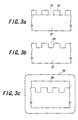
- Fig. 3a-3c are cross sectional views showing successive steps in producing an epitaxial growth substrate according to the present invention.
- a photoresist 22 is formed on a sapphire substrate 21 as a base material, and openings 23 are formed at the photoresist 22 by photolithography.
- the width of each opening is about 1 ⁇ m and the distance between the adjacent openings is about 1 ⁇ m.
- the sapphire substrate 21 is selectively etched via the remaining photoresist 22 as a mask to form plural ditches 24 in a strip shape, and then, the remaining photoresist 22 is removed.
- Dry etching process such as ion beam etching or reactive ion etching may be preferably employed as the etching process for the sapphire substrate, but wet etching process may be done.
- the width of the ditch 24 is determined on the width of the opening 23.
- the depth of the ditch 24 is determined on the etching time, and may be set to about 0.1 ⁇ m.
- the Al x Ga y In z N film 26 is laterally grown only on the convex portions of the concave-convex structure, not in the concave portions thereof because of the disturbance of the side walls of the plural strip-shaped ditches.
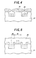
- the dislocations at the interface between the sapphire substrate 21 and the an Al x Ga y In z N film 26 are transmitted longitudinally, not laterally.
- the dislocations bends to the upper sides of the ditches constituting the concave-convex structure, so that there are small amount of dislocation at the areas W1 and W2 of the Al x Ga y In z N film 26. If the dislocation density at the interface between the sapphire substrate and the Al x Ga y In z N film 26 is about 10 10 cm 2 , in particular, the dislocation density at the areas W2 is about only 10 6 /cm 2 .
- the epitaxial growth substrate has a small amount of dislocation entirely, the plural Al a Ga b In c N films also have small amounts of dislocation, so that the light emitting element does not have undesired light absorption centers and can have high light emission efficiency.
- the above dislocation density-reducing effect becomes conspicuous as the Al content in the Al x Ga y In z N film constituting the epitaxial growth substrate according to the present invention is increased, particularly in the Al x Ga y In z N film with 50 atomic percents or over of Al, more particularly in the AlN film.
- ditches of the epitaxial growth substrate shown in Fig. 4 can be employed for scribe lines in cutting the substrate into plural pieces. Therefore, the thrive line-forming process can be emitted, resulting in the simplicity of the cutting process.
- Reactive Ion Etching was implemented on a C-faced sapphire substrate as a base material to form plural strip-shaped ditches having a width of about 1 ⁇ m and a depth of 0.2 ⁇ m.
- the sapphire substrate was heated to 1200°C, and trimethyl aluminum (TMA) and ammonium (NH 3 ) were introduced onto the sapphire substrate on condition that the pressure was 15 Torr and the flow rate ratio (NH 3 / TMA) was 450 to form an AlN film in a thickness of 2 ⁇ m.
- TMA trimethyl aluminum
- NH 3 ammonium
- the film-forming rate was about 1 ⁇ m.
- the dislocation density of the AlN film was about 10 6 /cm 2 in the whole range, so that it was turned out that the epitaxial growth substrate with the AlN film had a remarkably reduced dislocation density in comparison with a conventional one. Therefore, the thus obtained epitaxial growth substrate can be used for a light emitting element or the like.
- die above epitaxial growth substrate may be composed of a SiC substrate or a GaN substrate as a base material instead of the sapphire substrate.
- another electronicdevice such as a light emitting diode to emit another color light or ultraviolet light, a laser diode and a field effect transistor can be produced.
Landscapes
- Chemical & Material Sciences (AREA)
- Engineering & Computer Science (AREA)
- Crystallography & Structural Chemistry (AREA)
- Materials Engineering (AREA)
- Metallurgy (AREA)
- Organic Chemistry (AREA)
- Chemical Kinetics & Catalysis (AREA)
- General Chemical & Material Sciences (AREA)
- Inorganic Chemistry (AREA)
- Led Devices (AREA)
- Semiconductor Lasers (AREA)
- Crystals, And After-Treatments Of Crystals (AREA)
Applications Claiming Priority (4)
| Application Number | Priority Date | Filing Date | Title |
|---|---|---|---|
| JP32665099 | 1999-11-17 | ||
| JP32665099 | 1999-11-17 | ||
| JP2000344808A JP3455512B2 (ja) | 1999-11-17 | 2000-11-13 | エピタキシャル成長用基板およびその製造方法 |
| JP2000344808 | 2000-11-13 |
Publications (3)
| Publication Number | Publication Date |
|---|---|
| EP1101841A2 true EP1101841A2 (de) | 2001-05-23 |
| EP1101841A3 EP1101841A3 (de) | 2005-08-17 |
| EP1101841B1 EP1101841B1 (de) | 2011-06-29 |
Family
ID=26572250
Family Applications (1)
| Application Number | Title | Priority Date | Filing Date |
|---|---|---|---|
| EP00124938A Expired - Lifetime EP1101841B1 (de) | 1999-11-17 | 2000-11-15 | Verfahren zur Herstellung eines Epitaxie-Substrats |
Country Status (3)
| Country | Link |
|---|---|
| US (1) | US6426519B1 (de) |
| EP (1) | EP1101841B1 (de) |
| JP (1) | JP3455512B2 (de) |
Cited By (6)
| Publication number | Priority date | Publication date | Assignee | Title |
|---|---|---|---|---|
| WO2002023604A1 (en) * | 2000-09-18 | 2002-03-21 | Mitsubishi Cable Industries, Ltd. | Semiconductor base material and method of manufacturing the material |
| SG115549A1 (en) * | 2002-07-08 | 2005-10-28 | Sumitomo Chemical Co | Epitaxial substrate for compound semiconductor light emitting device, method for producing the same and light emitting device |
| CN1315200C (zh) * | 2001-07-24 | 2007-05-09 | 日亚化学工业株式会社 | 具有形成凹凸的基板的半导体发光元件 |
| US7683386B2 (en) | 2003-08-19 | 2010-03-23 | Nichia Corporation | Semiconductor light emitting device with protrusions to improve external efficiency and crystal growth |
| EP2528115A3 (de) * | 2011-05-24 | 2014-12-31 | Kabushiki Kaisha Toshiba | Lichtemittierendes Halbleiterbauelement, Nitrid-Halbleiterschicht und Verfahren zur Herstellung einer Nitrid-Halbleiterschicht |
| CN105070763A (zh) * | 2015-07-22 | 2015-11-18 | 中国科学院半导体研究所 | Soi叉指结构衬底ⅲ-ⅴ族材料沟道薄膜晶体管及制备方法 |
Families Citing this family (33)
| Publication number | Priority date | Publication date | Assignee | Title |
|---|---|---|---|---|
| DE60043122D1 (de) | 1999-03-17 | 2009-11-19 | Mitsubishi Chem Corp | Halbleiterbasis ihre Herstellung und Halbleiterkristallhersetllungsmethode |
| US6403451B1 (en) * | 2000-02-09 | 2002-06-11 | Noerh Carolina State University | Methods of fabricating gallium nitride semiconductor layers on substrates including non-gallium nitride posts |
| JP2002008985A (ja) * | 2000-06-21 | 2002-01-11 | Nichia Chem Ind Ltd | 窒化物半導体の製造方法及び窒化物半導体基板 |
| US6864158B2 (en) * | 2001-01-29 | 2005-03-08 | Matsushita Electric Industrial Co., Ltd. | Method of manufacturing nitride semiconductor substrate |
| JP2002231665A (ja) * | 2001-02-06 | 2002-08-16 | Sumitomo Metal Ind Ltd | エピタキシャル膜付き半導体ウエーハの製造方法 |
| US6562701B2 (en) * | 2001-03-23 | 2003-05-13 | Matsushita Electric Industrial Co., Ltd. | Method of manufacturing nitride semiconductor substrate |
| JP4092927B2 (ja) * | 2002-02-28 | 2008-05-28 | 豊田合成株式会社 | Iii族窒化物系化合物半導体、iii族窒化物系化合物半導体素子及びiii族窒化物系化合物半導体基板の製造方法 |
| JP4211358B2 (ja) * | 2002-11-01 | 2009-01-21 | 日亜化学工業株式会社 | 窒化物半導体、窒化物半導体素子及びそれらの製造方法 |
| US7012314B2 (en) * | 2002-12-18 | 2006-03-14 | Agere Systems Inc. | Semiconductor devices with reduced active region defects and unique contacting schemes |
| JP4823466B2 (ja) * | 2002-12-18 | 2011-11-24 | 日本碍子株式会社 | エピタキシャル成長用基板および半導体素子 |
| US20050110040A1 (en) * | 2003-11-26 | 2005-05-26 | Hui Peng | Texture for localizing and minimizing effects of lattice constants mismatch |
| JP3819398B2 (ja) * | 2004-04-27 | 2006-09-06 | 三菱電線工業株式会社 | 半導体発光素子およびその製造方法 |
| JP4712450B2 (ja) | 2004-06-29 | 2011-06-29 | 日本碍子株式会社 | AlN結晶の表面平坦性改善方法 |
| JP2006100787A (ja) * | 2004-08-31 | 2006-04-13 | Toyoda Gosei Co Ltd | 発光装置および発光素子 |
| US7633097B2 (en) * | 2004-09-23 | 2009-12-15 | Philips Lumileds Lighting Company, Llc | Growth of III-nitride light emitting devices on textured substrates |
| CN100454699C (zh) * | 2004-11-22 | 2009-01-21 | 松下电器产业株式会社 | 氮化合物系半导体装置及其制造方法 |
| JP4964430B2 (ja) * | 2005-05-25 | 2012-06-27 | 昭和電工株式会社 | 半導体素子形成用基板及びエピタキシャルウェーハ並びにそれらを利用した半導体素子及び半導体デバイス |
| JP2006332240A (ja) * | 2005-05-25 | 2006-12-07 | Sanyo Electric Co Ltd | 窒化物半導体発光素子の製造方法 |
| JP2007161525A (ja) * | 2005-12-14 | 2007-06-28 | Univ Of Tokushima | 半導体装置用基材およびその製造方法 |
| JP5084837B2 (ja) | 2006-10-18 | 2012-11-28 | ナイテック インコーポレイテッド | 深紫外線発光素子及びその製造方法 |
| JP2009059974A (ja) * | 2007-09-03 | 2009-03-19 | Univ Meijo | 半導体基板、半導体発光素子および半導体基板の製造方法 |
| US20090085055A1 (en) * | 2007-09-27 | 2009-04-02 | Hui Peng | Method for Growing an Epitaxial Layer |
| JP5306779B2 (ja) * | 2008-11-04 | 2013-10-02 | 学校法人 名城大学 | 発光素子及びその製造方法 |
| US8372738B2 (en) * | 2009-10-30 | 2013-02-12 | Alpha & Omega Semiconductor, Inc. | Method for manufacturing a gallium nitride based semiconductor device with improved termination scheme |
| TW201118946A (en) * | 2009-11-24 | 2011-06-01 | Chun-Yen Chang | Method for manufacturing free-standing substrate and free-standing light-emitting device |
| WO2011077541A1 (ja) | 2009-12-25 | 2011-06-30 | 創光科学株式会社 | エピタキシャル成長用テンプレート及びその作製方法 |
| EP2579297B1 (de) * | 2010-06-07 | 2020-12-16 | Soko Kagaku Co., Ltd. | Verfahren zur herstellung einer vorlage für epitaktisches wachstum und nitrid-halbleitervorrichtung |
| WO2015147135A1 (ja) | 2014-03-26 | 2015-10-01 | Jx日鉱日石エネルギー株式会社 | エピタキシャル成長用基板及びそれを用いた発光素子 |
| JP6212203B2 (ja) | 2014-04-14 | 2017-10-11 | 住友化学株式会社 | 窒化物半導体単結晶基板の製造方法 |
| JP5869064B2 (ja) * | 2014-07-17 | 2016-02-24 | 創光科学株式会社 | エピタキシャル成長用テンプレート及びその作製方法 |
| RU2653118C1 (ru) * | 2014-08-29 | 2018-05-07 | Соко Кагаку Ко., Лтд. | Шаблон для эпитаксиального выращивания, способ его получения и нитридное полупроводниковое устройство |
| KR101581169B1 (ko) | 2014-08-29 | 2015-12-29 | 소코 가가쿠 가부시키가이샤 | 에피택셜 성장용 템플릿 및 그 제조 방법, 그리고 질화물 반도체 장치 |
| JP7016044B2 (ja) * | 2018-04-26 | 2022-02-21 | パナソニックIpマネジメント株式会社 | Ramo4基板のエッチング方法 |
Citations (3)
| Publication number | Priority date | Publication date | Assignee | Title |
|---|---|---|---|---|
| EP0942459A1 (de) | 1997-04-11 | 1999-09-15 | Nichia Chemical Industries, Ltd. | Wachstumsmethode für einen nitrid-halbleiter, nitrid halbleitersubstrat und vorrichtung |
| EP0993048A2 (de) | 1998-09-14 | 2000-04-12 | Matsushita Electronics Corporation | Nitrid-Halbleitervorrichtung und ihr Herstellungsverfahren |
| EP1184897A1 (de) | 1999-03-17 | 2002-03-06 | Mitsubishi Cable Industries, Ltd. | Halbleiterbasis, ihre herstellungsmethode und halbleiterkristallherstellungsmethode |
Family Cites Families (10)
| Publication number | Priority date | Publication date | Assignee | Title |
|---|---|---|---|---|
| US5218216A (en) * | 1987-01-31 | 1993-06-08 | Toyoda Gosei Co., Ltd. | Gallium nitride group semiconductor and light emitting diode comprising it and the process of producing the same |
| US5787104A (en) * | 1995-01-19 | 1998-07-28 | Matsushita Electric Industrial Co., Ltd. | Semiconductor light emitting element and method for fabricating the same |
| JP2861991B2 (ja) * | 1997-10-20 | 1999-02-24 | 日亜化学工業株式会社 | 窒化ガリウム系化合物半導体チップの製造方法 |
| US6252253B1 (en) * | 1998-06-10 | 2001-06-26 | Agere Systems Optoelectronics Guardian Corp. | Patterned light emitting diode devices |
| JP3987660B2 (ja) | 1998-07-31 | 2007-10-10 | シャープ株式会社 | 窒化物半導体構造とその製法および発光素子 |
| JP3592553B2 (ja) * | 1998-10-15 | 2004-11-24 | 株式会社東芝 | 窒化ガリウム系半導体装置 |
| JP3594826B2 (ja) * | 1999-02-09 | 2004-12-02 | パイオニア株式会社 | 窒化物半導体発光素子及びその製造方法 |
| JP3471685B2 (ja) * | 1999-03-17 | 2003-12-02 | 三菱電線工業株式会社 | 半導体基材及びその製造方法 |
| JP4925497B2 (ja) * | 1999-06-28 | 2012-04-25 | フィリップス ルミレッズ ライティング カンパニー リミテッド ライアビリティ カンパニー | 半導体装置の組立方法およびiii−v族半導体装置 |
| JP3294223B2 (ja) * | 1999-08-18 | 2002-06-24 | 学校法人 名城大学 | 半導体の製造方法および該方法により製造した半導体素子 |
-
2000
- 2000-11-13 JP JP2000344808A patent/JP3455512B2/ja not_active Expired - Lifetime
- 2000-11-15 EP EP00124938A patent/EP1101841B1/de not_active Expired - Lifetime
- 2000-11-15 US US09/713,547 patent/US6426519B1/en not_active Expired - Lifetime
Patent Citations (3)
| Publication number | Priority date | Publication date | Assignee | Title |
|---|---|---|---|---|
| EP0942459A1 (de) | 1997-04-11 | 1999-09-15 | Nichia Chemical Industries, Ltd. | Wachstumsmethode für einen nitrid-halbleiter, nitrid halbleitersubstrat und vorrichtung |
| EP0993048A2 (de) | 1998-09-14 | 2000-04-12 | Matsushita Electronics Corporation | Nitrid-Halbleitervorrichtung und ihr Herstellungsverfahren |
| EP1184897A1 (de) | 1999-03-17 | 2002-03-06 | Mitsubishi Cable Industries, Ltd. | Halbleiterbasis, ihre herstellungsmethode und halbleiterkristallherstellungsmethode |
Cited By (24)
| Publication number | Priority date | Publication date | Assignee | Title |
|---|---|---|---|---|
| US7179667B2 (en) | 2000-09-18 | 2007-02-20 | Mitsubishi Cable Industries, Ltd. | Semiconductor base material and method of manufacturing the material |
| WO2002023604A1 (en) * | 2000-09-18 | 2002-03-21 | Mitsubishi Cable Industries, Ltd. | Semiconductor base material and method of manufacturing the material |
| US8344403B2 (en) | 2001-07-24 | 2013-01-01 | Nichia Corporation | Semiconductor light emitting device |
| US9368681B2 (en) | 2001-07-24 | 2016-06-14 | Nichia Corporation | Semiconductor light emitting device |
| US7635875B2 (en) | 2001-07-24 | 2009-12-22 | Nichia Corporation | Semiconductor light emitting device |
| US10593833B2 (en) | 2001-07-24 | 2020-03-17 | Nichia Corporation | Semiconductor light emitting device |
| US7745245B2 (en) | 2001-07-24 | 2010-06-29 | Nichia Corporation | Semiconductor light emitting device |
| US7804101B2 (en) | 2001-07-24 | 2010-09-28 | Nichia Corporation | Semiconductor light-emitting device |
| US10396242B2 (en) | 2001-07-24 | 2019-08-27 | Nichia Corporation | Semiconductor light emitting device |
| US8148744B2 (en) | 2001-07-24 | 2012-04-03 | Nichia Corporation | Semiconductor light emitting device |
| US8227280B2 (en) | 2001-07-24 | 2012-07-24 | Nichia Corporation | Semiconductor light emitting device |
| US8796721B2 (en) | 2001-07-24 | 2014-08-05 | Nichia Corporation | Semiconductor light emitting device |
| CN1315200C (zh) * | 2001-07-24 | 2007-05-09 | 日亚化学工业株式会社 | 具有形成凹凸的基板的半导体发光元件 |
| US8344402B2 (en) | 2001-07-24 | 2013-01-01 | Nichia Corporation | Semiconductor light emitting device |
| US8299486B2 (en) | 2001-07-24 | 2012-10-30 | Nichia Corporation | Semiconductor light emitting device |
| US9865773B2 (en) | 2001-07-24 | 2018-01-09 | Nichia Corporation | Semiconductor light emitting device |
| SG115549A1 (en) * | 2002-07-08 | 2005-10-28 | Sumitomo Chemical Co | Epitaxial substrate for compound semiconductor light emitting device, method for producing the same and light emitting device |
| US8119534B2 (en) | 2003-08-19 | 2012-02-21 | Nichia Corporation | Semiconductor light emitting device with protrusions to improve external efficiency and crystal growth |
| US7683386B2 (en) | 2003-08-19 | 2010-03-23 | Nichia Corporation | Semiconductor light emitting device with protrusions to improve external efficiency and crystal growth |
| US9190559B2 (en) | 2011-05-24 | 2015-11-17 | Kabushiki Kaisha Toshiba | Semiconductor light emitting device, nitride semiconductor layer, and method for forming nitride semiconductor layer |
| US9601662B2 (en) | 2011-05-24 | 2017-03-21 | Kabushiki Kaisha Toshiba | Semiconductor light emitting device, nitride semiconductor layer, and method for forming nitride semiconductor layer |
| EP2528115A3 (de) * | 2011-05-24 | 2014-12-31 | Kabushiki Kaisha Toshiba | Lichtemittierendes Halbleiterbauelement, Nitrid-Halbleiterschicht und Verfahren zur Herstellung einer Nitrid-Halbleiterschicht |
| CN105070763A (zh) * | 2015-07-22 | 2015-11-18 | 中国科学院半导体研究所 | Soi叉指结构衬底ⅲ-ⅴ族材料沟道薄膜晶体管及制备方法 |
| CN105070763B (zh) * | 2015-07-22 | 2017-10-03 | 中国科学院半导体研究所 | Soi叉指结构衬底ⅲ‑ⅴ族材料沟道薄膜晶体管及制备方法 |
Also Published As
| Publication number | Publication date |
|---|---|
| EP1101841B1 (de) | 2011-06-29 |
| US6426519B1 (en) | 2002-07-30 |
| EP1101841A3 (de) | 2005-08-17 |
| JP2001210598A (ja) | 2001-08-03 |
| JP3455512B2 (ja) | 2003-10-14 |
Similar Documents
| Publication | Publication Date | Title |
|---|---|---|
| US6426519B1 (en) | Epitaxial growth substrate and a method for producing the same | |
| US6790279B2 (en) | Method for manufacturing group III nitride compound semiconductor and a light-emitting device using group III nitride compound semiconductor | |
| Hiramatsu | Epitaxial lateral overgrowth techniques used in group III nitride epitaxy | |
| JP4743214B2 (ja) | 半導体素子およびその製造方法 | |
| US6533874B1 (en) | GaN-based devices using thick (Ga, Al, In)N base layers | |
| KR100623558B1 (ko) | Iii족 질화물계 화합물 반도체 및 그 제조방법 | |
| US6156581A (en) | GaN-based devices using (Ga, AL, In)N base layers | |
| US6599362B2 (en) | Cantilever epitaxial process | |
| US6617060B2 (en) | Gallium nitride materials and methods | |
| JP3036495B2 (ja) | 窒化ガリウム系化合物半導体の製造方法 | |
| US20200224331A1 (en) | High quality group-iii metal nitride crystals, methods of making, and methods of use | |
| US20100044719A1 (en) | III-V Compound Semiconductor Epitaxy Using Lateral Overgrowth | |
| KR20030070094A (ko) | 결정막, 결정기판 및 반도체장치 | |
| JPH10321911A (ja) | 単結晶シリコン上に化合物半導体のエピタキシヤル層を製造する方法及びそれにより製造された発光ダイオード | |
| JPH10312971A (ja) | III−V族化合物半導体膜とその成長方法、GaN系半導体膜とその形成方法、GaN系半導体積層構造とその形成方法、GaN系半導体素子とその製造方法 | |
| EP1376664A1 (de) | Verfahren zur herstellung eines halbleiters mit gruppe-iii-nitridzusammensetzung und halbleiterbauelement mit gruppe-iii-nitridzusammensetzung | |
| US20080296626A1 (en) | Nitride substrates, thin films, heterostructures and devices for enhanced performance, and methods of making the same | |
| US20010025989A1 (en) | Semiconductor device and method of manufacturing the same | |
| EP0709902B1 (de) | Lichtemittierende Halbleiteranordnung und Herstellungsverfahren | |
| US7893454B2 (en) | Method for producing structured substrate, structured substrate, method for producing semiconductor light emitting device, semiconductor light emitting device, method for producing semiconductor device, semiconductor device, method for producing device, and device | |
| EP1101842A2 (de) | Substrat für Epitaxie von III-V Verbindungshalbleitern und Verfahren zu seiner Herstellung | |
| JP3934320B2 (ja) | GaN系半導体素子とその製造方法 | |
| US8129260B2 (en) | Semiconductor substrates having low defects and methods of manufacturing the same | |
| JPH11274563A (ja) | 半導体装置および半導体発光素子 | |
| EP1047163A2 (de) | Halbleiterlaser, Halbleiterlaservorrichtung und Herstellungsverfahren |
Legal Events
| Date | Code | Title | Description |
|---|---|---|---|
| PUAI | Public reference made under article 153(3) epc to a published international application that has entered the european phase |
Free format text: ORIGINAL CODE: 0009012 |
|
| AK | Designated contracting states |
Kind code of ref document: A2 Designated state(s): AT BE CH CY DE DK ES FI FR GB GR IE IT LI LU MC NL PT SE TR |
|
| AX | Request for extension of the european patent |
Free format text: AL;LT;LV;MK;RO;SI |
|
| PUAL | Search report despatched |
Free format text: ORIGINAL CODE: 0009013 |
|
| AK | Designated contracting states |
Kind code of ref document: A3 Designated state(s): AT BE CH CY DE DK ES FI FR GB GR IE IT LI LU MC NL PT SE TR |
|
| AX | Request for extension of the european patent |
Extension state: AL LT LV MK RO SI |
|
| RIC1 | Information provided on ipc code assigned before grant |
Ipc: 7C 30B 25/18 B Ipc: 7H 01L 21/20 A Ipc: 7C 30B 29/40 B |
|
| 17P | Request for examination filed |
Effective date: 20050908 |
|
| AKX | Designation fees paid |
Designated state(s): DE FR GB |
|
| RIC1 | Information provided on ipc code assigned before grant |
Ipc: C30B 29/40 20060101ALI20100914BHEP Ipc: C30B 25/18 20060101ALI20100914BHEP Ipc: H01L 21/20 20060101ALI20100914BHEP Ipc: H01L 21/02 20060101AFI20100914BHEP |
|
| RTI1 | Title (correction) |
Free format text: A METHOD FOR PRODUCING AN EPITAXIAL GROWTH SUBSTRATE |
|
| GRAP | Despatch of communication of intention to grant a patent |
Free format text: ORIGINAL CODE: EPIDOSNIGR1 |
|
| GRAS | Grant fee paid |
Free format text: ORIGINAL CODE: EPIDOSNIGR3 |
|
| GRAA | (expected) grant |
Free format text: ORIGINAL CODE: 0009210 |
|
| AK | Designated contracting states |
Kind code of ref document: B1 Designated state(s): DE FR GB |
|
| REG | Reference to a national code |
Ref country code: GB Ref legal event code: FG4D |
|
| REG | Reference to a national code |
Ref country code: DE Ref legal event code: R096 Ref document number: 60046127 Country of ref document: DE Effective date: 20110818 |
|
| PLBE | No opposition filed within time limit |
Free format text: ORIGINAL CODE: 0009261 |
|
| STAA | Information on the status of an ep patent application or granted ep patent |
Free format text: STATUS: NO OPPOSITION FILED WITHIN TIME LIMIT |
|
| 26N | No opposition filed |
Effective date: 20120330 |
|
| GBPC | Gb: european patent ceased through non-payment of renewal fee |
Effective date: 20111115 |
|
| REG | Reference to a national code |
Ref country code: DE Ref legal event code: R097 Ref document number: 60046127 Country of ref document: DE Effective date: 20120330 |
|
| REG | Reference to a national code |
Ref country code: FR Ref legal event code: ST Effective date: 20120731 |
|
| PG25 | Lapsed in a contracting state [announced via postgrant information from national office to epo] |
Ref country code: GB Free format text: LAPSE BECAUSE OF NON-PAYMENT OF DUE FEES Effective date: 20111115 |
|
| PG25 | Lapsed in a contracting state [announced via postgrant information from national office to epo] |
Ref country code: FR Free format text: LAPSE BECAUSE OF NON-PAYMENT OF DUE FEES Effective date: 20111130 |
|
| PGFP | Annual fee paid to national office [announced via postgrant information from national office to epo] |
Ref country code: DE Payment date: 20191105 Year of fee payment: 20 |
|
| REG | Reference to a national code |
Ref country code: DE Ref legal event code: R071 Ref document number: 60046127 Country of ref document: DE |