EP1107324A2 - Verfahren zum Verbinden von Oxid-Supraleitern sowie die zugehörigen Supraleiterartikel - Google Patents
Verfahren zum Verbinden von Oxid-Supraleitern sowie die zugehörigen Supraleiterartikel Download PDFInfo
- Publication number
- EP1107324A2 EP1107324A2 EP00126012A EP00126012A EP1107324A2 EP 1107324 A2 EP1107324 A2 EP 1107324A2 EP 00126012 A EP00126012 A EP 00126012A EP 00126012 A EP00126012 A EP 00126012A EP 1107324 A2 EP1107324 A2 EP 1107324A2
- Authority
- EP
- European Patent Office
- Prior art keywords
- base materials
- oxide superconductor
- solder
- oxide
- joining
- Prior art date
- Legal status (The legal status is an assumption and is not a legal conclusion. Google has not performed a legal analysis and makes no representation as to the accuracy of the status listed.)
- Granted
Links
Images


Classifications
-
- H—ELECTRICITY
- H10—SEMICONDUCTOR DEVICES; ELECTRIC SOLID-STATE DEVICES NOT OTHERWISE PROVIDED FOR
- H10N—ELECTRIC SOLID-STATE DEVICES NOT OTHERWISE PROVIDED FOR
- H10N60/00—Superconducting devices
- H10N60/80—Constructional details
-
- Y—GENERAL TAGGING OF NEW TECHNOLOGICAL DEVELOPMENTS; GENERAL TAGGING OF CROSS-SECTIONAL TECHNOLOGIES SPANNING OVER SEVERAL SECTIONS OF THE IPC; TECHNICAL SUBJECTS COVERED BY FORMER USPC CROSS-REFERENCE ART COLLECTIONS [XRACs] AND DIGESTS
- Y02—TECHNOLOGIES OR APPLICATIONS FOR MITIGATION OR ADAPTATION AGAINST CLIMATE CHANGE
- Y02E—REDUCTION OF GREENHOUSE GAS [GHG] EMISSIONS, RELATED TO ENERGY GENERATION, TRANSMISSION OR DISTRIBUTION
- Y02E40/00—Technologies for an efficient electrical power generation, transmission or distribution
- Y02E40/60—Superconducting electric elements or equipment; Power systems integrating superconducting elements or equipment
-
- Y—GENERAL TAGGING OF NEW TECHNOLOGICAL DEVELOPMENTS; GENERAL TAGGING OF CROSS-SECTIONAL TECHNOLOGIES SPANNING OVER SEVERAL SECTIONS OF THE IPC; TECHNICAL SUBJECTS COVERED BY FORMER USPC CROSS-REFERENCE ART COLLECTIONS [XRACs] AND DIGESTS
- Y10—TECHNICAL SUBJECTS COVERED BY FORMER USPC
- Y10S—TECHNICAL SUBJECTS COVERED BY FORMER USPC CROSS-REFERENCE ART COLLECTIONS [XRACs] AND DIGESTS
- Y10S505/00—Superconductor technology: apparatus, material, process
- Y10S505/825—Apparatus per se, device per se, or process of making or operating same
- Y10S505/917—Mechanically manufacturing superconductor
-
- Y—GENERAL TAGGING OF NEW TECHNOLOGICAL DEVELOPMENTS; GENERAL TAGGING OF CROSS-SECTIONAL TECHNOLOGIES SPANNING OVER SEVERAL SECTIONS OF THE IPC; TECHNICAL SUBJECTS COVERED BY FORMER USPC CROSS-REFERENCE ART COLLECTIONS [XRACs] AND DIGESTS
- Y10—TECHNICAL SUBJECTS COVERED BY FORMER USPC
- Y10S—TECHNICAL SUBJECTS COVERED BY FORMER USPC CROSS-REFERENCE ART COLLECTIONS [XRACs] AND DIGESTS
- Y10S505/00—Superconductor technology: apparatus, material, process
- Y10S505/825—Apparatus per se, device per se, or process of making or operating same
- Y10S505/917—Mechanically manufacturing superconductor
- Y10S505/918—Mechanically manufacturing superconductor with metallurgical heat treating
-
- Y—GENERAL TAGGING OF NEW TECHNOLOGICAL DEVELOPMENTS; GENERAL TAGGING OF CROSS-SECTIONAL TECHNOLOGIES SPANNING OVER SEVERAL SECTIONS OF THE IPC; TECHNICAL SUBJECTS COVERED BY FORMER USPC CROSS-REFERENCE ART COLLECTIONS [XRACs] AND DIGESTS
- Y10—TECHNICAL SUBJECTS COVERED BY FORMER USPC
- Y10S—TECHNICAL SUBJECTS COVERED BY FORMER USPC CROSS-REFERENCE ART COLLECTIONS [XRACs] AND DIGESTS
- Y10S505/00—Superconductor technology: apparatus, material, process
- Y10S505/825—Apparatus per se, device per se, or process of making or operating same
- Y10S505/917—Mechanically manufacturing superconductor
- Y10S505/918—Mechanically manufacturing superconductor with metallurgical heat treating
- Y10S505/919—Reactive formation of superconducting intermetallic compound
-
- Y—GENERAL TAGGING OF NEW TECHNOLOGICAL DEVELOPMENTS; GENERAL TAGGING OF CROSS-SECTIONAL TECHNOLOGIES SPANNING OVER SEVERAL SECTIONS OF THE IPC; TECHNICAL SUBJECTS COVERED BY FORMER USPC CROSS-REFERENCE ART COLLECTIONS [XRACs] AND DIGESTS
- Y10—TECHNICAL SUBJECTS COVERED BY FORMER USPC
- Y10S—TECHNICAL SUBJECTS COVERED BY FORMER USPC CROSS-REFERENCE ART COLLECTIONS [XRACs] AND DIGESTS
- Y10S505/00—Superconductor technology: apparatus, material, process
- Y10S505/825—Apparatus per se, device per se, or process of making or operating same
- Y10S505/917—Mechanically manufacturing superconductor
- Y10S505/918—Mechanically manufacturing superconductor with metallurgical heat treating
- Y10S505/919—Reactive formation of superconducting intermetallic compound
- Y10S505/92—Utilizing diffusion barrier
-
- Y—GENERAL TAGGING OF NEW TECHNOLOGICAL DEVELOPMENTS; GENERAL TAGGING OF CROSS-SECTIONAL TECHNOLOGIES SPANNING OVER SEVERAL SECTIONS OF THE IPC; TECHNICAL SUBJECTS COVERED BY FORMER USPC CROSS-REFERENCE ART COLLECTIONS [XRACs] AND DIGESTS
- Y10—TECHNICAL SUBJECTS COVERED BY FORMER USPC
- Y10S—TECHNICAL SUBJECTS COVERED BY FORMER USPC CROSS-REFERENCE ART COLLECTIONS [XRACs] AND DIGESTS
- Y10S505/00—Superconductor technology: apparatus, material, process
- Y10S505/825—Apparatus per se, device per se, or process of making or operating same
- Y10S505/917—Mechanically manufacturing superconductor
- Y10S505/925—Making superconductive joint
-
- Y—GENERAL TAGGING OF NEW TECHNOLOGICAL DEVELOPMENTS; GENERAL TAGGING OF CROSS-SECTIONAL TECHNOLOGIES SPANNING OVER SEVERAL SECTIONS OF THE IPC; TECHNICAL SUBJECTS COVERED BY FORMER USPC CROSS-REFERENCE ART COLLECTIONS [XRACs] AND DIGESTS
- Y10—TECHNICAL SUBJECTS COVERED BY FORMER USPC
- Y10S—TECHNICAL SUBJECTS COVERED BY FORMER USPC CROSS-REFERENCE ART COLLECTIONS [XRACs] AND DIGESTS
- Y10S505/00—Superconductor technology: apparatus, material, process
- Y10S505/825—Apparatus per se, device per se, or process of making or operating same
- Y10S505/917—Mechanically manufacturing superconductor
- Y10S505/926—Mechanically joining superconductive members
-
- Y—GENERAL TAGGING OF NEW TECHNOLOGICAL DEVELOPMENTS; GENERAL TAGGING OF CROSS-SECTIONAL TECHNOLOGIES SPANNING OVER SEVERAL SECTIONS OF THE IPC; TECHNICAL SUBJECTS COVERED BY FORMER USPC CROSS-REFERENCE ART COLLECTIONS [XRACs] AND DIGESTS
- Y10—TECHNICAL SUBJECTS COVERED BY FORMER USPC
- Y10S—TECHNICAL SUBJECTS COVERED BY FORMER USPC CROSS-REFERENCE ART COLLECTIONS [XRACs] AND DIGESTS
- Y10S505/00—Superconductor technology: apparatus, material, process
- Y10S505/825—Apparatus per se, device per se, or process of making or operating same
- Y10S505/917—Mechanically manufacturing superconductor
- Y10S505/927—Metallurgically bonding superconductive members
-
- Y—GENERAL TAGGING OF NEW TECHNOLOGICAL DEVELOPMENTS; GENERAL TAGGING OF CROSS-SECTIONAL TECHNOLOGIES SPANNING OVER SEVERAL SECTIONS OF THE IPC; TECHNICAL SUBJECTS COVERED BY FORMER USPC CROSS-REFERENCE ART COLLECTIONS [XRACs] AND DIGESTS
- Y10—TECHNICAL SUBJECTS COVERED BY FORMER USPC
- Y10T—TECHNICAL SUBJECTS COVERED BY FORMER US CLASSIFICATION
- Y10T29/00—Metal working
- Y10T29/49—Method of mechanical manufacture
- Y10T29/49002—Electrical device making
- Y10T29/49014—Superconductor
Definitions
- the present invention relates to a method of joining together oxide superconductors for producing an oxide superconductor joined member having excellent electric current transmission performance, enabling electric current transmission to be effected at high efficiency, and to the oxide superconductor joined member having excellent electric current transmission performance, so that electric current lead wires and superconducting wire rods, excellent in electric current transmission performance, can be produced.
- oxide superconductors having high critical temperatures such as, for example, LiTi 2 O 3 , Ba(Bi, Pb)O 3 , (Ba, K) BiO 3 , (La, Sr) 2 CuO 4 , REBa 2 Cu 3 O 7 (RE refers to rare-earth elements), Bi 2 Sr 2 Ca 2 Cu 3 O 10 , Ti 2 Ba 2 Ca 2 Cu 3 O 10 or HgBa 2 Ca 2 Cu 3 O 8 and so forth, one after another.
- RE refers to rare-earth elements
- a RE 123-type oxide crystal that is, a "RE Ba 2 Cu 3 O y oxide superconductor (RE refers to one kind of rare-earth element, or not less than two kinds of rare-earth elements, selected from the group consisting of Y, La, Pr, Nd, Sm, Eu, Gd, Dy, Ho, Er, Tm, and Yb)" not only has a high critical temperature but also has come to attain a high critical current density in a magnetic field due to development of, and improvement on manufacturing techniques, so that the same is one of superconductors attracting most attention lately.
- RE refers to one kind of rare-earth element, or not less than two kinds of rare-earth elements, selected from the group consisting of Y, La, Pr, Nd, Sm, Eu, Gd, Dy, Ho, Er, Tm, and Yb
- the melt-solidifying process is a process utilizing solidification from a half- molten state, whereby a raw material for the bulk crystal from which the constitution of an RE 123-type oxide superconductor can be obtained normally in the atmosphere or in an atmosphere containing oxygen at low partial pressure is heated to not lower than a temperature (a peritectic point) at which a "123 phase (referred to hereinafter as RE 123 phase) of an RE Ba 2 Cu 3 O x oxide to be prepared" undergoes decomposition and melting, thereby causing the raw material to be decomposed and melted, and thereafter, is subjected to slow and gradual cooling at a temperature gradient or in an isothermal state, or is maintained in a supercooled temperature zone where growth of the RE 123 phase can take place, thereby promoting growth of the bulk crystal.
- a method of dipping a seed in a melt is commonly adopted in order to determine an orientation of the crystal to be grown.
- the super cooled melt-solidifying process is a process whereby a molten precursor material is supercooled in as-molten state or as-half-molten state to a temperature zone below a solidification temperature, and is subjected to gradual cooling from a temperature reached as above or is kept at the temperature reached, thereby implementing crystal growth, and is a process intended to enhance a crystal growth speed by supercooling.
- the oxide superconductor crystal obtained by those processes described above, and so forth, has been found to be material which is brittle and lacking in plasticity, and consequently, it has been difficult to form the same into a current lead wire, wire rod, and the like, of long length, by taking advantage of plasticity.
- oxide superconductor rods and "a conductive material coated with an oxide superconductor” by joining together a plurality of the oxide superconductor crystals.
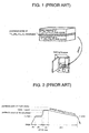
- Fig. 1 is a schematic view illustrating a manner whereby the powdered solder of Yb 123 superconductor material constitution(that is, Yb211 + Ba 3 Cu 5 O x ) is held in a sandwich-like fashion between the base materials of the Y 123-type superconducting bulk crystal, and these materials are then placed in a heating furnace for joining together the base materials through heating and gradual cooling.
- heating and gradual cooling of the materials are carried out in the heating furnace according to a heating and cooling curve shown in Fig. 2 by way of example.
- bubbles, impurities, and so forth are often contained in the solder which has turned into a liquid phase in a half-molten state, and these too tend to remain in the form of a layer within the finally solidified portion after turned into voids, and the like.
- Fig. 3 is a schematic view illustrating the "pushing phenomenon".
- the solder in half-molten state is in a condition containing grains of the Yb 211 phase, bubbles, and so forth, in a BaO - CuO melt as shown in Fig. 3 (a).
- an oxide superconductor joined member produced by the means of joining together as described in the foregoing interferes with transmission of superconducting current, and noticeably reduces current passing therethrough, so that a superconducting current lead wire and superconducting wire rod, produced by use of the oxide superconductor joined member, has been incapable of exhibiting fully satisfactory performance.
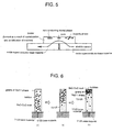
- Fig. 5 is a schematic view illustrating an example of an oxide superconductor joined member prepared by disposing a solder on the upper surface of base materials so as to straddle both the base materials brought adjacently to each other, like bridge-building, instead of sandwiching the solder between the base materials, and by joining together the base materials through gradual cooling of the solder after heating and melting the same.
- the oxide superconductor joined member is made up so as to have a "constitution wherein the oxide superconductor base materials are joined with each other on at least a face thereof, other than the butting surface thereof, through the intermediary of a binder"
- the binder In the case of using the vapor deposited film, and the like, as the binder, it is not necessarily required to use an oxide superconductor, having a low melting point, as the vapor deposited film, so that the same kind of superconductor as the base materials may be used.
- the invention has been developed based on the above-described items, and so forth of the knowledge, and an object of the invention is to provide "a method of joining together oxide superconductors", and “an oxide superconductor joined member produced by the same” as follows.
- the RE 123-type superconducting bulk crystal (RE Ba 2 Cu 3 O y bulk crystal: RE refers to one kind or not less than two kinds of rare earth elements, selected from the group consisting of Y, La, Pr, Nd, Sm, Eu, Gd, Dy, Ho, Er, Tm, and Yb) which has been limited in application because of poor formability in spite of its high critical temperature and high critical current density is preferably used as the base materials.
- the RE 123-type superconducting bulk crystal can have considerably expanded application.
- an oxide superconducting material having a melting point lower than that of the base materials, and having the same crystal structure as that of the base materials is preferably used as the solder used for joining together the oxide superconductor base materials.
- the material is preferably rendered into powdered form in consideration of fusibility.
- Table 1 shows a fusion (precursor) form and peritectic point (melting point) with reference to typical RE 123-type superconducting materials by way of example.
- an RE 123 superconducting material having a peritectic point (melting point) lower than that of the base materials is selected as the solder.
- RE 123-type superconductor material fusion form peritectic (K) point (°C) Yb 123 Yb 211 + Ba 3 Cu 5 O y (1248K) (965°C) Y 123 Y 211 + Ba 3 Cu 5 O y (1278K) (1005°C) Sm 123 Sm 211 + Ba 3 Cu 5 O y (1333K) (1060°C) Nd 123 Nd 211 + Ba 3 Cu 5 O y (1363K) (1090°C)
- ingenuities are applied to a position of solder placement or to the shape of a junction face of the respective oxide superconductor base materials.
- one of the ingenuities is represented by a configuration of "disposing the solder on the upper surface of the base materials so as to straddle both the base materials brought adjacently to each other, like bridge-building, instead of holding the solder sandwiched between the base materials" as previously described with reference to Fig. 5.
- Fig. 6 is a schematic view illustrating the behavior of the solder at the junction when joining together of the base materials is carried out by disposing the solder on the upper surface of the base materials so as to straddle both the base materials brought adjacently to each other, like bridge-building.
- solder in a half-molten state is in a condition wherein grains of Yb 211 phase, pores, and so forth are contained in a BaO - CuO melt as shown in Fig. 6 (a).
- the segregation layer of non-superconducting inclusions is not formed on the base material side of the binder formed by crystallization and solidification of solder, so that a transmission path of superconducting electric current, having no obstacle present therein, is secured inside a joined member of Y 123 superconducting bulk crystals.
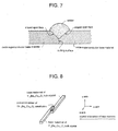
- oxide superconductor base materials may have butting surfaces such that at least portions of the butting surfaces are shaped in a sloped open face, parting from each other, as shown in Fig. 7, by way of example.
- joining together of the base materials is implemented by overlaying the solder on the sloped open face of the respective base materials, and solidification of the soldering material starts from the sloped face of the respective base materials in the course of gradual cooling after heating. Meanwhile, as crystallization proceeds in the direction of the normal to the respective sloped face, the non-superconducting particles, micropores, impurity constituents, and so forth which are present in the soldering material are pushed in the direction of the normal to the respective sloped face, thereby being subjected to segregation on the outer surface of the solder.
- the segregation layer of the non-superconducting inclusions is not formed in this case either on the base material side of the binder formed by crystallization and solidification of solder, so that the transmission path of superconducting electric current, having no obstacle present therein, is secured inside the joined member of the superconducting bulk crystals.
- a single crystal (bulk crystal) of an oxide superconducting material has a crystal lattice arranged in a single direction, and consequently, has strong anisotropy, so that, if external force is applied thereto, the single crystal normally undergoes cleavage on a given crystal surface (in the case of RE 123-type oxide superconductor, the ab face thereof becomes a cleavage surface). Accordingly, crystal orientation is aligned across the entire cleavage surface thereof.
- the orientation of the binder formed as a result of solidification of the solder can be aligned with that of the base materials without paying special attention to positioning of the binder as well as the base materials, so that a joined member having excellent superconductive properties can be obtained with ease.
- the binder (oxide superconducting material) making up the junction may be the vapor deposited film obtained by, for example, the vacuum deposition method.
- the makeup of the junction is not a butt-joined structure, and is inevitably at a disadvantage in terms of time required, however, it is possible to implement a junction whereby an excellent transmission path of superconducting electric current can be secured by depositing the vapor deposited films in layers, formed by use of the vacuum deposition method, and so forth, like bridge-building.
- the vapor deposited film, and the like, as the binder there is no need of using necessarily an oxide superconductor, having a melting point lower than that of the base materials, for the vapor deposited film, and accordingly, the same type of oxide superconductor as the base materials can be adopted therefor.
- the above-described means of joining together oxide superconductors capable of obtaining excellent current transmission performance can be not only applicable to production of current lead wires made up of an oxide superconductor and superconducting wire rods, but also adopted as a method of joining together oxide superconductor thick filmed wire rods (LPE wire rods), and a method of repairing a coating of members coated with an oxide superconductor film.
- LPE wire rods oxide superconductor thick filmed wire rods
- Y 123 superconducting bulk crystals (Y 1.8 Ba 2.4 Cu 3.4 O y ) were prepared by a melt-solidifying process.
- a square member was cut from the Y 123 superconducting bulk crystals, respectively, by machining, and an attempt was made to join together two pieces of the square members as base materials to be joined together by use of a solder.
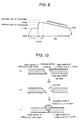
- the base materials When joining together the base materials, the base materials were first laid such that a side face of one of the base materials, at one end thereof, was kept in intimate contact with a side face of another of the base materials, at one end thereof, so as to overlap each other as shown in Fig. 8, and the solder in powder form was overlaid on top of the overlapped part of the base materials so as to straddle both the base materials like bridge-building.
- the base materials as overlapped were placed in a heating furnace, and subjected to heating and gradual cooling, thereby joining together the base materials by crystallizing the solder, and turning the same into a bridge-building-type Yb 123 superconducting binder.
- Fig. 9 shows a heating and cooling curve thereof at this point in time.
- Nd 123 superconducting bulk crystals (NdBa 2 Cu 3 O y ) were prepared by a melt-solidifying process.
- a square member was cut from the Nd 123 superconducting bulk crystals, respectively, by machining, and an attempt was made to join together two pieces of the square members as base materials to be joined together by use of a solder.
- powders (powders of Sm 211 + Ba 3 Cu 5 O x ) of Sm 123 superconducting material (SmBa 2 Cu 5 O y ) constitution were used.
- the respective base materials were first cleaved at one end thereof as shown in Fig. 10 (a), exposing respective cleavage surfaces (ab faces), and thereafter, a portion of the end of one of the base materials was cut off as shown in Fig. 10 (b).
- the base materials as butt-joined were placed in a heating furnace, and subjected to heating and gradual cooling, thereby joining together the base materials by crystallizing the solder, and turning the same into a bridge-building-type Sm 123 superconductor binder.
- Fig. 11 shows a heating and cooling curve thereof at this point in time.
- the base materials in this case are set at the time of the joining process such that the cleavage surfaces at the respective ends are butted at each other, the crystal orientations of both the base materials as they are aligned with each other, so that there hardly occurs any disarray to Sm 123 superconducting crystals (binder) which grow starting from the end surface of the respective base materials.
- the invention it is possible to provide an oxide superconductor joined member, excellent in electric current transmission performance, without a need of going through particularly complex steps, so that the invention can bring about very useful effects from an industrial point of view such as making significant contributions to enhancement in performance of superconducting current lead materials, superconducting wire rods, and so forth.
Landscapes
- Superconductors And Manufacturing Methods Therefor (AREA)
- Manufacturing Of Electrical Connectors (AREA)
- Superconductor Devices And Manufacturing Methods Thereof (AREA)
Applications Claiming Priority (2)
| Application Number | Priority Date | Filing Date | Title |
|---|---|---|---|
| JP34159699 | 1999-12-01 | ||
| JP34159699A JP2001155566A (ja) | 1999-12-01 | 1999-12-01 | 超電導体の接合方法及び超電導体接合部材 |
Publications (3)
| Publication Number | Publication Date |
|---|---|
| EP1107324A2 true EP1107324A2 (de) | 2001-06-13 |
| EP1107324A3 EP1107324A3 (de) | 2004-12-01 |
| EP1107324B1 EP1107324B1 (de) | 2007-07-18 |
Family
ID=18347313
Family Applications (1)
| Application Number | Title | Priority Date | Filing Date |
|---|---|---|---|
| EP00126012A Expired - Lifetime EP1107324B1 (de) | 1999-12-01 | 2000-11-28 | Verfahren zum Verbinden von Oxid-Supraleitern sowie die zugehörigen Supraleiterartikel |
Country Status (4)
| Country | Link |
|---|---|
| US (1) | US6561412B2 (de) |
| EP (1) | EP1107324B1 (de) |
| JP (1) | JP2001155566A (de) |
| DE (1) | DE60035568T2 (de) |
Cited By (2)
| Publication number | Priority date | Publication date | Assignee | Title |
|---|---|---|---|---|
| EP1949996A3 (de) * | 2007-01-25 | 2009-06-03 | United Technologies Corporation | Diffusionslötreparatur von Metallkomponenten |
| EP3104374A4 (de) * | 2014-02-04 | 2017-10-18 | Riken | Verbindungskörper mit geringem widerstand für supraleitendes hochtemperaturdrahtmaterial und verbindungsverfahren |
Families Citing this family (8)
| Publication number | Priority date | Publication date | Assignee | Title |
|---|---|---|---|---|
| US7608785B2 (en) * | 2004-04-27 | 2009-10-27 | Superpower, Inc. | System for transmitting current including magnetically decoupled superconducting conductors |
| US7071148B1 (en) | 2005-04-08 | 2006-07-04 | Superpower, Inc. | Joined superconductive articles |
| US8716188B2 (en) | 2010-09-15 | 2014-05-06 | Superpower, Inc. | Structure to reduce electroplated stabilizer content |
| JP5934352B2 (ja) | 2011-06-21 | 2016-06-15 | カウンシル オブ サイエンティフィク アンド インダストリアル リサーチ | 改良超伝導ペーストを用いた(bi,pb)−2223酸化物高温超伝導体の管の接合方法 |
| TWI458145B (zh) | 2011-12-20 | 2014-10-21 | Ind Tech Res Inst | 超導材料的接合方法 |
| KR101374177B1 (ko) * | 2012-10-11 | 2014-03-14 | 케이조인스(주) | 고온 초전도체층의 직접 접촉에 의한 부분 미세 용융 확산 압접을 이용한 2세대 ReBCO 고온 초전도체의 접합 및 산소 공급 어닐링 열처리에 의한 초전도 회복 방법 |
| JP6108888B2 (ja) | 2013-03-13 | 2017-04-05 | 古河電気工業株式会社 | ピーラブル超電導導体、ピーラブル超電導導体の製造方法及び超電導線の補修方法 |
| US10706991B2 (en) * | 2015-02-12 | 2020-07-07 | Sumitomo Electric Industries, Ltd. | Method for producing a superconducting wire material lengthened |
Family Cites Families (17)
| Publication number | Priority date | Publication date | Assignee | Title |
|---|---|---|---|---|
| US3144704A (en) * | 1962-07-02 | 1964-08-18 | Ibm | Method of making couplings to super-conductor circuits |
| DE1803804C3 (de) * | 1968-10-18 | 1973-09-27 | Kernforschungsanlage Juelich Gmbh, 5170 Juelich | Thermogenerator zur Erzeugung von Gleichstrom fur supraleitende Strom kreise |
| JPS59107586A (ja) * | 1982-12-13 | 1984-06-21 | Nippon Telegr & Teleph Corp <Ntt> | 超伝導フリツプチツプボンデイング方法 |
| JPS6164084A (ja) * | 1984-09-06 | 1986-04-02 | 三菱電機株式会社 | 超電導機器 |
| US4713878A (en) * | 1984-12-05 | 1987-12-22 | General Electric Company | Mold method for superconductive joint fabrication |
| AU600156B2 (en) * | 1987-08-06 | 1990-08-02 | University Of Arkansas, The | Meltable high temperature superconductor |
| US5051397A (en) * | 1988-11-25 | 1991-09-24 | Hitachi, Ltd. | Joined body of high-temperature oxide superconductor and method of joining oxide superconductors |
| US5874175A (en) * | 1988-11-29 | 1999-02-23 | Li; Chou H. | Ceramic composite |
| US5075253A (en) * | 1989-04-12 | 1991-12-24 | Advanced Micro Devices, Inc. | Method of coplanar integration of semiconductor IC devices |
| US5034373A (en) * | 1989-12-22 | 1991-07-23 | Inco Alloys International, Inc. | Process for forming superconductor precursor |
| US5244876A (en) * | 1990-02-13 | 1993-09-14 | Hoechst Aktiengesellschaft | Method for joining parts of ceramic high-temperature superconductor material |
| CA2038012A1 (en) * | 1990-03-14 | 1991-09-15 | Hideki Shimizu | Oxide superconductor lamination and method of manufacturing the same |
| FR2678432B1 (fr) * | 1991-06-27 | 1993-09-03 | Alsthom Gec | Procede de liaison entre une ceramique supraconductrice a haute temperature critique et un conducteur supraconducteur a base de niobium-titane. |
| US5786304A (en) * | 1992-04-03 | 1998-07-28 | Nippon Steel Corporation | Joining product of oxide superconducting material and process for producing the same |
| JP3034378B2 (ja) | 1992-05-25 | 2000-04-17 | 財団法人国際超電導産業技術研究センター | Y系酸化物超電導体結晶の作製方法 |
| DE69938283T2 (de) * | 1998-11-13 | 2009-03-05 | International Superconductivity Technology Center | Verfahren zur Herstellung einer Verbindung zwischen supraleitendem Oxyd und normalem Leiter |
| US6159905A (en) * | 1999-06-02 | 2000-12-12 | Buzcek; David M. | Methods for joining high temperature superconducting components with negligible critical current degradation and articles of manufacture in accordance therewith |
-
1999
- 1999-12-01 JP JP34159699A patent/JP2001155566A/ja active Pending
-
2000
- 2000-11-28 EP EP00126012A patent/EP1107324B1/de not_active Expired - Lifetime
- 2000-11-28 DE DE60035568T patent/DE60035568T2/de not_active Expired - Lifetime
- 2000-11-30 US US09/726,263 patent/US6561412B2/en not_active Expired - Fee Related
Cited By (2)
| Publication number | Priority date | Publication date | Assignee | Title |
|---|---|---|---|---|
| EP1949996A3 (de) * | 2007-01-25 | 2009-06-03 | United Technologies Corporation | Diffusionslötreparatur von Metallkomponenten |
| EP3104374A4 (de) * | 2014-02-04 | 2017-10-18 | Riken | Verbindungskörper mit geringem widerstand für supraleitendes hochtemperaturdrahtmaterial und verbindungsverfahren |
Also Published As
| Publication number | Publication date |
|---|---|
| DE60035568T2 (de) | 2008-04-10 |
| US20010015371A1 (en) | 2001-08-23 |
| US6561412B2 (en) | 2003-05-13 |
| EP1107324A3 (de) | 2004-12-01 |
| JP2001155566A (ja) | 2001-06-08 |
| DE60035568D1 (de) | 2007-08-30 |
| EP1107324B1 (de) | 2007-07-18 |
Similar Documents
| Publication | Publication Date | Title |
|---|---|---|
| AU599807B2 (en) | Method of fabricating a superconductive body, and apparatus and systems comprising the body | |
| US6635097B2 (en) | Biaxially textured articles formed by powder metallurgy | |
| US6447714B1 (en) | Method for forming biaxially textured articles by powder metallurgy | |
| US5972846A (en) | Article comprising textured superconductive cuprate material | |
| US6610414B2 (en) | Biaxially textured articles formed by power metallurgy | |
| EP0423375B1 (de) | Oxydsupraleiter und verfahren zur herstellung | |
| EP0634379B1 (de) | Verbundprodukt supraleitender oxidwerkstoffe und seine herstellung | |
| EP1107324B1 (de) | Verfahren zum Verbinden von Oxid-Supraleitern sowie die zugehörigen Supraleiterartikel | |
| CA1263449A (en) | Method of manufacturing a superconductor compounds layer | |
| JP4113113B2 (ja) | 酸化物超電導体の接合方法及び酸化物超電導体接合体 | |
| US20100009855A1 (en) | Process for joining oxide superconducting tubes with a superconducting joint | |
| KR920005516B1 (ko) | 산화물 초전도 재료를 구비한 물체의 제조방법 | |
| US5310704A (en) | Method of manufacturing superconductive conductor | |
| US6929695B2 (en) | Method for preparing single crystal oxide thin film | |
| KR970005161B1 (ko) | 초전도체 제조방법과 장치 | |
| JPH1192143A (ja) | 超電導ウィスカーおよびその製造方法 | |
| Xu et al. | FLUX PINNING AND CRITICAL CURRENTS IN SUPERCONDUCTOR-NORMAL METAL COMPOSITES | |
| JPH07254473A (ja) | 酸化物超電導体同士の超電導接続状態を形成する方法 | |
| JPH06131923A (ja) | 傾斜異相濃度酸化物超電導導体及びその製造方法 | |
| JPH0467692A (ja) | 超伝導素子 | |
| JPH03290307A (ja) | 酸化物超電導体厚膜テープ材料の製造方法 | |
| JPH0645140A (ja) | 酸化物超電導体電流リード | |
| JPH05129669A (ja) | 超伝導素子 |
Legal Events
| Date | Code | Title | Description |
|---|---|---|---|
| PUAI | Public reference made under article 153(3) epc to a published international application that has entered the european phase |
Free format text: ORIGINAL CODE: 0009012 |
|
| AK | Designated contracting states |
Kind code of ref document: A2 Designated state(s): AT BE CH CY DE DK ES FI FR GB GR IE IT LI LU MC NL PT SE TR |
|
| AX | Request for extension of the european patent |
Free format text: AL;LT;LV;MK;RO;SI |
|
| PUAL | Search report despatched |
Free format text: ORIGINAL CODE: 0009013 |
|
| RIC1 | Information provided on ipc code assigned before grant |
Ipc: 7H 01R 4/68 B Ipc: 7H 01L 39/24 A |
|
| AK | Designated contracting states |
Kind code of ref document: A3 Designated state(s): AT BE CH CY DE DK ES FI FR GB GR IE IT LI LU MC NL PT SE TR |
|
| AX | Request for extension of the european patent |
Extension state: AL LT LV MK RO SI |
|
| 17P | Request for examination filed |
Effective date: 20050408 |
|
| 17Q | First examination report despatched |
Effective date: 20050513 |
|
| AKX | Designation fees paid |
Designated state(s): DE FR GB |
|
| 17Q | First examination report despatched |
Effective date: 20050513 |
|
| GRAP | Despatch of communication of intention to grant a patent |
Free format text: ORIGINAL CODE: EPIDOSNIGR1 |
|
| GRAS | Grant fee paid |
Free format text: ORIGINAL CODE: EPIDOSNIGR3 |
|
| GRAA | (expected) grant |
Free format text: ORIGINAL CODE: 0009210 |
|
| AK | Designated contracting states |
Kind code of ref document: B1 Designated state(s): DE FR GB |
|
| REG | Reference to a national code |
Ref country code: GB Ref legal event code: FG4D |
|
| REF | Corresponds to: |
Ref document number: 60035568 Country of ref document: DE Date of ref document: 20070830 Kind code of ref document: P |
|
| ET | Fr: translation filed | ||
| PLBE | No opposition filed within time limit |
Free format text: ORIGINAL CODE: 0009261 |
|
| STAA | Information on the status of an ep patent application or granted ep patent |
Free format text: STATUS: NO OPPOSITION FILED WITHIN TIME LIMIT |
|
| 26N | No opposition filed |
Effective date: 20080421 |
|
| PGFP | Annual fee paid to national office [announced via postgrant information from national office to epo] |
Ref country code: FR Payment date: 20121130 Year of fee payment: 13 Ref country code: DE Payment date: 20121121 Year of fee payment: 13 |
|
| PGFP | Annual fee paid to national office [announced via postgrant information from national office to epo] |
Ref country code: GB Payment date: 20121128 Year of fee payment: 13 |
|
| GBPC | Gb: european patent ceased through non-payment of renewal fee |
Effective date: 20131128 |
|
| REG | Reference to a national code |
Ref country code: FR Ref legal event code: ST Effective date: 20140731 |
|
| PG25 | Lapsed in a contracting state [announced via postgrant information from national office to epo] |
Ref country code: DE Free format text: LAPSE BECAUSE OF NON-PAYMENT OF DUE FEES Effective date: 20140603 |
|
| REG | Reference to a national code |
Ref country code: DE Ref legal event code: R119 Ref document number: 60035568 Country of ref document: DE Effective date: 20140603 |
|
| PG25 | Lapsed in a contracting state [announced via postgrant information from national office to epo] |
Ref country code: GB Free format text: LAPSE BECAUSE OF NON-PAYMENT OF DUE FEES Effective date: 20131128 Ref country code: FR Free format text: LAPSE BECAUSE OF NON-PAYMENT OF DUE FEES Effective date: 20131202 |