EP1107449A2 - Kompensationsschaltung für nichtlineare Verzerrungen, sowie zugehörige Sendevorrichtung und mobiles Kommunikationsgerät - Google Patents
Kompensationsschaltung für nichtlineare Verzerrungen, sowie zugehörige Sendevorrichtung und mobiles Kommunikationsgerät Download PDFInfo
- Publication number
- EP1107449A2 EP1107449A2 EP00125434A EP00125434A EP1107449A2 EP 1107449 A2 EP1107449 A2 EP 1107449A2 EP 00125434 A EP00125434 A EP 00125434A EP 00125434 A EP00125434 A EP 00125434A EP 1107449 A2 EP1107449 A2 EP 1107449A2
- Authority
- EP
- European Patent Office
- Prior art keywords
- transmission power
- transmission
- compensation
- power control
- control information
- Prior art date
- Legal status (The legal status is an assumption and is not a legal conclusion. Google has not performed a legal analysis and makes no representation as to the accuracy of the status listed.)
- Granted
Links
Images


Classifications
-
- H—ELECTRICITY
- H03—ELECTRONIC CIRCUITRY
- H03F—AMPLIFIERS
- H03F1/00—Details of amplifiers with only discharge tubes, only semiconductor devices or only unspecified devices as amplifying elements
- H03F1/32—Modifications of amplifiers to reduce non-linear distortion
- H03F1/3241—Modifications of amplifiers to reduce non-linear distortion using predistortion circuits
- H03F1/3247—Modifications of amplifiers to reduce non-linear distortion using predistortion circuits using feedback acting on predistortion circuits
-
- H—ELECTRICITY
- H03—ELECTRONIC CIRCUITRY
- H03F—AMPLIFIERS
- H03F1/00—Details of amplifiers with only discharge tubes, only semiconductor devices or only unspecified devices as amplifying elements
- H03F1/32—Modifications of amplifiers to reduce non-linear distortion
- H03F1/3241—Modifications of amplifiers to reduce non-linear distortion using predistortion circuits
- H03F1/3282—Acting on the phase and the amplitude of the input signal
- H03F1/3288—Acting on the phase and the amplitude of the input signal to compensate phase shift as a function of the amplitude
-
- H—ELECTRICITY
- H03—ELECTRONIC CIRCUITRY
- H03F—AMPLIFIERS
- H03F1/00—Details of amplifiers with only discharge tubes, only semiconductor devices or only unspecified devices as amplifying elements
- H03F1/32—Modifications of amplifiers to reduce non-linear distortion
- H03F1/3241—Modifications of amplifiers to reduce non-linear distortion using predistortion circuits
- H03F1/3294—Acting on the real and imaginary components of the input signal
-
- H—ELECTRICITY
- H03—ELECTRONIC CIRCUITRY
- H03F—AMPLIFIERS
- H03F2201/00—Indexing scheme relating to details of amplifiers with only discharge tubes, only semiconductor devices or only unspecified devices as amplifying elements covered by H03F1/00
- H03F2201/32—Indexing scheme relating to modifications of amplifiers to reduce non-linear distortion
- H03F2201/3233—Adaptive predistortion using lookup table, e.g. memory, RAM, ROM, LUT, to generate the predistortion
Definitions
- the present invention relates generally to a non-linear distortion compensation circuit, a transmitter device to be employed in the same and a mobile communication unit. More particularly, the invention relates to a control system for a non-linear distortion compensation circuit for compensating non-linear distortion to be caused by non-linearity of an amplifier or a frequency converter.
- a linearizer as a non-linear distortion compensation circuit for compensating non-linear distortion caused by non-linearity of an amplifier, a frequency converter or the like forming a transmitter to be used in a radio communication.
- the linearizer one taking output only non-linear signal from a transmission signal transmitted and compensating non-linear distortion by subtracting the taken out non-linear distortion signal, or one preliminarily multiplying a signal having distortion compensating characteristics to a transmission signal before radio transmission process, such as frequency conversion, amplification and so forth with taking a non-linear distortion to be caused in the transmitter into account, for compensating distortion.
- non-linear distortion caused by non-linearity of the amplifier, frequency converter and so forth forming the transmitter to be used in radio communication appears as a leak current in a frequency band of a channel on transmission and in a frequency band of an adjacent channel of the channel on transmission and the leak current increases according of increasing of transmission power.
- a power leaking to adjacent channel is known as an adjacent-channel leak power.
- the adjacent-channel leak power caused by the transmitter may affect for other radio equipment communicating using the adjacent channel to cause degradation of reception characteristics.
- CDMA system Code Division Multiple Access system
- the CDMA system spreading of spectra of communication signals is performed employing a spreading code, such as pseudo noise code (PN code: Pseudo random Noise code), and communication signals are identified by the spreading code. Therefore, the CDMA system is characterized by capability of simultaneous communication of a plurality of radio equipments and a plurality of channels at the same frequency.
- PN code pseudo noise code
- the CDMA system is also characterized by the fact that, upon demodulating a received signal, demodulation of the received signal cannot be accomplished unless multiplying the same spreading code as that used in spreading on transmission side at the same timing as that in the transmission side, and the received signal spread by different spreading code or the received signal spread at different timing, namely the signals used for communication by other radio equipments or the signals of other channels are fallen as noise within a reception band currently on reception.
- a base station of mobile communication where a plurality of mobile stations are present in distal position and proximal position of the base station and where communication is performed by CDMA system.
- the transmission power of the mobile station communicating at the proximal position of the base station is higher than that of the mobile station communicating at the distal position to submerge the transmission signal of the mobile station at the distal position in the transmission signal of the mobile station at the proximal position. This has been known as a far-near problem.
- the transmission signal of the distal mobile station cannot be demodulated correctly since the signal of the proximal mobile station falls with the reception band as noise.
- the far-near problem is solved by performing transmission power control at high precision and high accuracy relatively frequently. Namely, by performing transmission power control, a transmission power of the proximal mobile station is controlled to be lower power and a transmission power of the distal mobile station is controlled to be higher power.
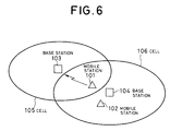
- the frequency converter and/or the amplifier forming the transmitter of the mobile station has to be operated at non-linear region thereof. As a result, non-linear distortion of the transmission signal increases at higher level of the transmission power. Namely, the adjacent-channel leak power transmitted from the transmitter is increased. Influence of the adjacent-channel leak power to other system will be discussed with reference to Fig. 6.
- Fig. 6 illustrates a mobile communication system including a mobile station 101, a mobile station 102, a base station 103, a base station 104, a cell 105 and a cell 106.
- the cell 105 represents a service area of the base station 103 and is extended in the vicinity of the base station 104.
- the cell 106 is the service area of the base station 104.
- the transmission power and the adjacent-channel leak power of the mobile station 101 increase according to traveling toward the distal position by transmission power control of the base station 103 to the mobile station 101.
- the transmission power and the adjacent-channel leak power of the mobile station 101 arrive to the base station 104 at higher power.
- the transmission power transmitted from the mobile station 102 may submerge in the adjacent-channel leak power transmitted from the mobile station 101, In such case, a problem is encountered in that the base station 104 cannot receive the signal of the mobile station 102 correctly. This is because that the transmission power of the mobile station 102 is lower power for transmission power control of the base station 104 in the mobile station 102.
- a linearizer for compensating non-linear distortion of the transmitter is employed.
- the linearizer one taking output only non-linear signal from a transmission signal transmitted and compensating non-linear distortion by subtracting the taken out non-linear distortion signal, or one preliminarily multiplying a signal having distortion compensating characteristics to a transmission signal before radio transmission process, such as frequency conversion, amplification and so forth with taking a non-linear distortion to be caused in the transmitter into account, for compensating distortion.
- the former is not practical for increasing of current consumption due to increasing of circuit scale and for complexity of process. Therefore, the latter is primarily used as the non-linear distortion compensation circuit.
- the later linearizer is called as pre-distortion type linearizer.
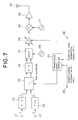
- Fig. 7 Prior art used in such pre-distortion type linearizer is shown in Fig. 7. It should be noted that the construction shown in Fig. 7 has been disclosed in Japanese Unexamined Patent Publication No. Heisei 10-23095.
- a transmission signal is consisted with two-system of data, i.e. digital I data and Q data which are supplied to respective input terminals 21 and 22. These input data are supplied to a pre-distorter 25 via FIR filters 23 and 24 to obtain digital I data and Q data superimposed an inverted component of the non-linear distortion caused by a variable power amplifier 29.
- a transmission power control signal from a transmission power controller 34 is supplied in addition to I and Q data.
- the pre-distorter 25 derives the inverted component of the non-linear distortion by arithmetic process on the basis of the transmission power control signal and I and Q data. The inverted component thus derived is superimposed on the I and Q data.
- An output data of the pre-distorter 25 is converted into an analog signal by a D/A converter 26 and then is modulated by the modulator 27 with an output of an oscillator 28.
- I and Q signals (data) are modulated by orthogonal modulation.
- spreading process by the spreading code is performed by the modulator 27.
- the transmission signal thus modulated by spreading is supplied to a variable power amplifier 29 to be amplified with an amplifier gain determined by a transmission power control signal from a transmission power controller 34.
- a transmission power control signal from a transmission power controller 34.
- An amplified output is mixed with an oscillation frequency from a frequency synthesizer 31 in a mixer 30 and then is transmitted as radio signal from an antenna 33 with amplification with a given gain by an amplifier 32.
- the transmission power control signal output from the transmission power controller 34 is generated on the basis of a power control information bit input from a terminal 35 and a reception level information signal input from a terminal 36.
- the power control information bit is a power control information bit data contained in the signal transmitted to own radio transmitter device from a counterpart (generally, the base station) to communicate.
- a reception level information signal is information of a reception level of a reception signal transmitted from the base station.
- occurrence condition of non-linear distortion in the power amplifier 29 variable of amplifier gain can be accurately judged by the pre-distorter 25. Then, on the basis of occurrence condition of the non-linear distortion as judged, compensation component as inverted component of the non-linear distortion can be generated. With the compensation component, even when the amplifier gain is varied by the power amplifier 29, accurate distortion compensation corresponding to the amplifier gain can be performed.
- the base station may discriminate the channel on reception or the mobile station in communication by the spreading code. Therefore, the base station may discriminate a power of a desired wave on reception and power of other reception signals, from the reception signal and thus can derive S/N ratio of the channel on reception.
- Transmission power control is performed depending upon the S/N ratio of the channel on reception. Namely, the base station derives a power of the desired wave and a power of interfering wave for deriving the S/N ratio of the channel on reception.
- the base station When the S/N ratio is less than or equal to the predetermined value, the base station transmits the control signal for increasing power of the transmission signal of the mobile station to the mobile station. On the other hand, when the S/N ratio is greater than the predetermined value, the base station transmits the information for reducing the transmission power so that the transmission power of the mobile station on communication will not interfere communication of other mobile station in communication. Calculation of S/N ratio executed by the base station is performed per time slot forming the transmission frame transmitted by the base station. Thus, the transmission control information is updated per time slot. A relationship between the transmission frame transmitted by the base station and the transmission power control information transmitted is shown in Fig. 8. Process of transmission power control to be executed will be discussed with reference to Fig. 8.
- one frame to be transmitted is consisted of n in number of time slots TS1 to TSn.
- One slot is consisted of the control information, transmission power control information and communication data.
- the mobile station on reception of the signal transmitted by the base station demodulats to extract the transmission power control information from the demodulated reception signal and performs transmission power control of the transmitter per time slot.
- the compensation of the non-linear distortion performed on the basis of detected transmission power of the signal transmitted in the time slot TSi at a certain timing may compensate distortion of the transmission signal transmitted in the next time slot TS(i+1).
- the transmission signal transmitted in the time slot TS(i+1) is differentiated the transmission power from the transmission power in the time slot TSi by the transmission power control, correct non-linear distortion compensation cannot be performed.
- the non-linear distortion compensation to be performed on the basis of detected transmission power transmitted in the time slot TSi at a certain timing is effected for distortion compensation of the transmission signal of the transmission in the next time slot TS(i+1).
- the transmission power transmitted in the time slot TS(i+1) is differentiated from the transmission power of the time slot TSi, correct non-linear distortion compensation cannot be performed.
- An object of the present invention is to provide a non-linear distortion compensation circuit, a transmission equipment employing the same and a mobile transmission equipment, in which a mobile station can accurately compensate distortion caused by non-linearity of a transmitter per bit (symbol) even while the base station is performing transmission power control for the transmitter of the mobile station.
- a non-linear distortion compensation circuit in a transmission equipment for controlling a transmission power depending upon an external transmission power control information upon transmission of a digital signal comprises:
- a transmission equipment comprises:
- a mobile communication equipment comprises:
- the compensation component generating means may generate the compensation component per bit, and the compensation means may perform compensation of the non-linear distortion according to the compensation component per bit.
- the compensation component generating means may calculate the transmission power per bit on the basis of an instantaneous transmission power value and an average value of the transmission power, and generate the compensation component per bit according to the result of calculation and the transmission power control information.
- the compensation component generating means may comprise storage means for preliminarily storing a compensation data as the compensation component and address generating means for generating an address of the storage means on the basis of the transmission power per bit and the transmission power control information.
- the address generating means may be constructed to generate the address by addition of the transmission power per bit and the transmission power control information.
- the address generating means may derive the transmission power per bit is calculated by addition of an instantaneous transmission power and an average value of the transmission power.
- the transmission signal may be a time slot type
- the external transmission power control information may be set for controlling the transmission power per transmission time slot
- the address generating means may derive the transmission power per bit by addition of an average power value of a transmission time slot at a certain timing and an instantaneous power value per each bit of subsequent transmission time slot.
- the transmission power control information may be information for transmission power control for subsequent transmission time slot.
- the storage means may be a read-only memory.
- the transmission power control signal may be respectively superimposed per time slot of the signal transmitted from the base station.
- ROM address depending upon the transmission power per bit of the transmission signal and the transmission power control information is generated by the address generating portion generating the address of the compensation data storage ROM storing the non-linear distortion data to be used for performing non-linear distortion by the pre-distortion type linearizer.
- the transmission power control information may reflect the time slot as control object.
- Fig. 1 is a schematic block diagram showing an overall construction of the preferred embodiment of a mobile station according to the present invention.
- a reception signal from the antenna 1 is input to a receiving portion 3 via an antenna multicoupler 2 for reception process to be extracted I and Q components of a base band signal.
- the I and Q components thus extracted to are input to a demodulating portion 4 for demodulation process (despreading process), and then is output from a speaker 6 as a audible sound after error correction in an error correcting portion 5.
- a voice signal from a microphone 7 is converted into a digital signal by a transmission signal generating portion 8 and then subject to a linear modulation process (generally, QPSK modulation process) to be lead as signals of I and Q components. Subsequently, compensation of non-linear distortion is performed by a pre-distortion type linearizer 9. Then, transmission process is performed by a transmitting portion 10. Thereafter, a radio wave signal as a transmission signal is transmitted through the antenna via a directional coupler 11 and the antenna multicoupler 2.
- a linear modulation process generally, QPSK modulation process
- the transmission signal branched by the directional coupler 11 is derived by an average power value per time slot of the transmission signal input to an average power calculating portion 12.
- the I and Q components as output of the transmission signal generating portion 8 is input to an instantaneous power calculating portion 13.
- the instantaneous transmission power is calculated per bit (symbol).
- the transmission power control information is detected from output of the error correcting portion 5 by a transmission power control information detecting portion 15. It should be noted that the transmission power control information is not supplied to the speaker 6.
- Respective outputs of the average power calculating portion 12, the instantaneous power calculating portion 13 and the transmission power control information detecting portion 15 are supplied to an address generating portion 14 for generating an address for accessing a compensation data storage ROM 16. By the address thus generated, a compensation data is read out to be supplied to the pre-distortion type linearizer 9.
- the transmitting portion 10 is constructed with a D/A converter 501, an orthogonal modulator 502, a variable gain amplifier 503, an intermediate band pass filter 504, a frequency converter (mixer) 505, a first radio frequency band pass filter 506, an amplifier 507, a second radio frequency band pass filter 508, a transmission amplifier 509, a first local oscillator 510 and a second local oscillator 511.
- the D/A converter 501 converts the transmission signal of an intermediate band from digital signal to analog signal.
- the orthogonal modulator 502 performs orthogonal modulation of the transmission signal of the base band and performs frequency conversion into a transmission signal in the intermediate frequency band.
- the variable gain amplifier 503 is an amplifier for amplifying the transmission signal according to received transmission power control information.
- the intermediate frequency band pass filter 504 is a filter passing the transmission signal of the intermediate frequency band.
- the frequency converter 505 performs frequency conversion of the transmission signal of intermediate frequency band into the transmission signal of radio frequency band.
- the first radio frequency band pass filter 506 and the second radio frequency band pass filter 508 are filters passing only signal of a transmission band and suppressing unnecessary radiation caused in the frequency amplifier 505 or the amplifier 507.
- the amplifier 507 is an amplifier amplifying the transmission signal.
- the transmission amplifier 509 is an amplifier for amplifying the transmission signal up to a power for transmission through the antenna.
- the first local oscillator 510 is an oscillator for oscillating a local oscillation signal to be used upon frequency conversion in the frequency converter 505.
- the second local oscillator 511 is an oscillator oscillating a local oscillation signal to be used upon frequency oscillation in the orthogonal modulator 502.
- I and Q component signal input ends of the D/A converter 501 match with I and Q component signal input ends of the transmitting portion 10 and an output end of the transmission amplifier 509 matchs with an output end of the transmitting portion 10.
- the I and Q component signal output ends of the D/A converter 501 are connected to the I and Q component signal input ends of the orthogonal modulator 502.
- An intermediate frequency band signal output end of the orthogonal modulator 502 is connected to an input end of the variable gain amplifier 503.
- An output end of the variable gain amplifier 503 is connected to an input end of the intermediate frequency band pass filter 504.
- An output end of the intermediate frequency band pass filter 504 is connected to an intermediate frequency band signal input end of the frequency converter 505.
- a radio frequency band output end of the frequency converter 505 is connected to an input end of the first radio frequency band pass filter 506.
- An output end of the first radio frequency band pass filter 506 is connected to an input end of the amplifier 507.
- An output end of the amplifier 507 is connected to an input end of the second radio frequency band pass filter 508.
- An output end of the second radio frequency band pass filter 508 is connected to an input end of the transmission amplifier 509.
- an output end of the first local oscillator 510 is connected to a local signal input end of the frequency converter 505.
- An output end of the second local oscillator 511 is connected to a local signal input end of the orthogonal modulator 502.
- a gain control signal input end of the variable gain amplifier 503 is connected to a transmission power control information output end of a transmission power control information modulator 401.
- the time slot TSi is received from the base station (step S11).
- demodulating portion 4 demodulation process of the time slot TSi is performed (step S12).
- error correcting portion 5 error correction process of the time slot TSi is performed in the error correcting portion 5 (step S13).
- next time slot TS(i+1) is received (step S14).
- the transmission power control information is extracted from the received signal of the time slot TSi (step S31) to be output to the address generating portion 14. It should be noted that the transmission power control information is a control information for controlling the transmission power of the transmission time slot TS(i+1) on the transmission side.
- step S11 On reception side, when the time slot TSi is received at step S11, signal processing for the transmitted data, such as error correction and so forth, is effected for the transmission data, such as voice or the like for the transmission time slot TS(i+1) and the transmission frame is generated according to a transmission frame format. Thereafter, the transmission signal is spread using the spreading code. The spread transmission signal is output separately as I component and Q component signals (step S21).
- the transmission signals of I component and Q component output from the transmission signal generating portion 8 is input to the pre-distortion type linearizer 9.
- the transmission signals of I component and Q component are also input to the instantaneous power calculating portion 13. In the instantaneous power calculating portion 13, instantaneous powers of the input I component signal and Q component signal (step 32) are derived to output to the address generator 14.
- the I component and Q component signals input to the pre-distortion type linearizer 9 are compensated non-linear distortion by the non-linear distortion compensation data read out from the compensation data storage ROM 16 (step S36) and are output to the transmitting portion 10. Operation of the transmitting portion 10 will be discussed with reference to Fig. 2.
- the I component and Q component signals input to the transmitting portion 10 are converted from digital signal into analog signal by the D/A converter 501.
- the orthogonal modulator 502 performs orthogonal modulation for the I component and Q component signals output from the D/A converter 501 using local oscillation signal oscillated by the second local oscillator 511, and the transmission signal of the base band is converted into the transmission signal of the intermediate frequency band.
- the transmission signal converted into the transmission signal of the intermediate frequency band is amplified according to the transmission power control information by the variable gain amplifier 503 and then input to the frequency converter 505 via the intermediate frequency band pass filter 504.
- the gain of the variable gain amplifier 503 is variable depending upon transmission power control information output by the transmission power control information detecting portion 15.
- the frequency converter 505 performs frequency conversion of the input transmission signal of the intermediate frequency band into the transmission signal of radio frequency band using the local oscillation frequency oscillated by the first local oscillator 510.
- the transmission signal of the radio frequency band thus converted passes through the first radio frequency band pass filter 506, the amplifier 507, the second radio frequency band pass filter 508, amplified upon to the power to be transmitted through antenna 1 by the transmission amplifier 509 and then is output from the transmitting portion 10.
- the transmission signal thus output from the transmitting portion is input to the directional coupler 11 and is output from an inserting direction output end to be transmitted through the antenna 1, and in conjunction therewith, is output from a coupling direction output end to be input to an average power calculating portion 12.
- an average power per unit time slot of the input transmission signal is derived to output the result of detection for the address generating portion 14.
- transmission of the transmission time slot TSi is transmitted (step S23).
- an average value of the transmission power of the transmission time slot TSi is derived in the average power calculating portion 12 (step S34) to be output to the address generating portion 14.
- the address for accessing the compensation data storage ROM 16 is generated using the result of calculation output from the instantaneous power calculating portion 13, the result of calculation output from the average power calculating portion 12 and the transmission power control information output from the transmission power control information detecting portion 15 (step S35) to designate the address of ROM 16.
- ROM 16 outputs the non-linear distortion compensation data according to the address designated by the address generating portion 14 to the pre-distortion type linearizer 9.
- step S23 process for compensating non-linear distortion of the I component and Q component signals to transmit using the non-linear distortion compensation data input from the compensation data storage ROM 16 (step S23). Then, preparation for transmission of the next time slot TS(I+1) is performed (step S24).
- the signal to be transmitted can be expressed as a function of amplitude and phase.
- the characteristics of the power amplifier in the transmitting portion 10 is expressed as characteristics of both of amplitude and phase as shown in Fig. 4. Namely, by increasing of the output power, characteristics of amplitude and phase are degraded to cause non-linear distortion. Therefore, it can be said that the non-linear distortion is amplitude distortion for amplitude of the transmission signal and phase distortion for the phase of the transmission signal.
- the non-linear distortion to be caused in the transmitter 206 can be canceled by providing components of - ⁇ A and - ⁇ P to the transmission signal.
- the non-linear compensation data stored in the compensation data storage ROM 16 has to be data having inverted characteristics of amplitude distortion and phase distortion to be caused in the transmitting portion 10.
- the compensation data may be read out from ROM with taking the derived transmission power as address.
- the transmission power per bit of the transmission time slot TS(i+1) is derived using the average transmission power of certain time slot TSi, instantaneous powers of I component and Q component to be transmitted in the next time slot TS(i+1) and the transmission power control information for the time slot TS(i+1).
- the correct transmission power value per bit to be transmitted finally is derived by adding the instantaneous power value (per bit) of the transmission in the time slot TS(i+1) to be compensated to the average transmission power value of the one preceding transmission time slot TSi for deriving the transmission power value per bit, and to the sum thus derived, adding the transmission power control information for the transmission time slot TS(i+1).
- Fig. 5 (1) represents control information
- (2) represents the transmission power control information
- (3) represents the communication data, respectively.
- the upper level shows reception time slots and the lower level shows transmission time slots.
- the transmission power control information received at the reception time slot TS(i+1) becomes effective in the transmission time slot TS(i+1).
- the average power calculated by the average power calculating portion 12 becomes the average power of the transmission signal of the transmission time slot TSi.
- the transmission signal of the transmission time slot TSi is on transmission, and naturally, the transmission signal has past through the pre-distortion type linearizer 9.
- the transmission signal of the next transmission time slot TS(i+1) is input for compensation for distortion.
- ROM address for taking the distortion compensation data is generated on the basis of the average power of the transmission signal, the instantaneous power of the transmission signal and the transmission power control information (to be added). Accordingly, as a result, the average power of the transmission signal is an average power of the transmission time slot TSi , the instantaneous power of the transmission signal is the instantaneous power of the transmission time slot TS(i+1), and for interpolation of this, the transmission power control information for the transmission time slot TS(i+1) is used.
- the non-linear distortion compensation data of the transmitting portion 10 is derived preliminarily and are corresponded to the transmission power in one-by-one basis to establish correspondence between the transmission power and the compensation data ROM 16.
- the address of the compensation data storage ROM 16 storing the data for compensating the non-linear distortion is generated using the instantaneous power calculated from the I component and Q component signals to be transmitted, the average transmission power per unit slot of the transmission signal and the transmission power control information. Then the non-linear distortion compensation data is taken out from the compensation data storage ROM 16 to provide non-linear compensation for the transmission signal by the pre-distortion type linearizer.
- non-linear distortion in the transmitting portion of the mobile communication equipment is compensated using the pre-distortion type linearizer per bit (symbol) of the transmission power. Furthermore, since compensation is performed with taking the transmission power control information from the base station into account, more accurate compensation operation of the non-linear distortion can be performed.
Landscapes
- Physics & Mathematics (AREA)
- Nonlinear Science (AREA)
- Engineering & Computer Science (AREA)
- Power Engineering (AREA)
- Transmitters (AREA)
- Digital Transmission Methods That Use Modulated Carrier Waves (AREA)
- Mobile Radio Communication Systems (AREA)
Applications Claiming Priority (2)
| Application Number | Priority Date | Filing Date | Title |
|---|---|---|---|
| JP33891799A JP3381689B2 (ja) | 1999-11-30 | 1999-11-30 | 非線形歪み補償回路及びそれを用いた送信装置並びに移動通信機 |
| JP33891799 | 1999-11-30 |
Publications (3)
| Publication Number | Publication Date |
|---|---|
| EP1107449A2 true EP1107449A2 (de) | 2001-06-13 |
| EP1107449A3 EP1107449A3 (de) | 2005-10-19 |
| EP1107449B1 EP1107449B1 (de) | 2007-10-03 |
Family
ID=18322558
Family Applications (1)
| Application Number | Title | Priority Date | Filing Date |
|---|---|---|---|
| EP20000125434 Expired - Lifetime EP1107449B1 (de) | 1999-11-30 | 2000-11-20 | Kompensationsschaltung für nichtlineare Verzerrungen, sowie zugehörige Sendevorrichtung und mobiles Kommunikationsgerät |
Country Status (6)
| Country | Link |
|---|---|
| US (1) | US6741867B1 (de) |
| EP (1) | EP1107449B1 (de) |
| JP (1) | JP3381689B2 (de) |
| CN (1) | CN1199479C (de) |
| AU (1) | AU772463B2 (de) |
| DE (1) | DE60036596T2 (de) |
Cited By (5)
| Publication number | Priority date | Publication date | Assignee | Title |
|---|---|---|---|---|
| WO2004064248A1 (en) * | 2003-01-13 | 2004-07-29 | Telefonaktiebolaget L M Ericsson (Publ) | Device and method for predistorting an input signal |
| EP1455444A1 (de) * | 2003-01-13 | 2004-09-08 | Telefonaktiebolaget LM Ericsson (publ) | Vorrichtung und Verfahren zum Vorverzerrung eines Eingangssignals |
| EP1742351A1 (de) | 2005-07-07 | 2007-01-10 | Hitachi Kokusai Electric Inc. | Vorverzerrungsverstärker |
| WO2011072299A1 (en) * | 2009-12-11 | 2011-06-16 | Qualcomm Incorporated | Baseband compensation for phase discontinuities in radio frequency communication devices |
| EP1634400A4 (de) * | 2003-06-06 | 2012-02-29 | Interdigital Tech Corp | Einstellung der amplituden- und phaseneigenschaften von sendererzeugten drahtlosen kommunikationssignalen als reaktion auf basisstations-sendeleistungssteuersignale und bekannte sender-verstärkereigenschaften |
Families Citing this family (47)
| Publication number | Priority date | Publication date | Assignee | Title |
|---|---|---|---|---|
| JP2000349640A (ja) * | 1999-06-02 | 2000-12-15 | Nec Corp | 符号分割多重化送信装置 |
| US7012968B2 (en) * | 2000-11-30 | 2006-03-14 | Lg Electronics, Inc. | Apparatus for detecting and adjusting transmission power of CDMA system |
| US7570709B2 (en) * | 2001-03-08 | 2009-08-04 | Siemens Aktiengesellschaft | Automatic transmit power control loop with modulation averaging |
| US7039125B2 (en) * | 2001-03-12 | 2006-05-02 | Analog Devices, Inc. | Equalized SNR power back-off |
| KR100438445B1 (ko) * | 2001-03-22 | 2004-07-03 | 삼성전자주식회사 | 비선형 왜곡 보상 방법 및 비선형 왜곡 보상 회로 |
| US7362818B1 (en) * | 2001-08-30 | 2008-04-22 | Nortel Networks Limited | Amplitude and phase comparator for microwave power amplifier |
| JP3850736B2 (ja) * | 2002-02-06 | 2006-11-29 | 富士通株式会社 | 無線信号を利用して伝送される情報を判定する装置およびその方法 |
| US20030157905A1 (en) * | 2002-02-18 | 2003-08-21 | Matsushita Electric Industrial Co., Ltd. | Transmitter and associated method for reducing the adjacent channel power during wireless communications |
| US8380143B2 (en) | 2002-05-01 | 2013-02-19 | Dali Systems Co. Ltd | Power amplifier time-delay invariant predistortion methods and apparatus |
| US6985704B2 (en) | 2002-05-01 | 2006-01-10 | Dali Yang | System and method for digital memorized predistortion for wireless communication |
| US8811917B2 (en) | 2002-05-01 | 2014-08-19 | Dali Systems Co. Ltd. | Digital hybrid mode power amplifier system |
| US8472897B1 (en) | 2006-12-22 | 2013-06-25 | Dali Systems Co. Ltd. | Power amplifier predistortion methods and apparatus |
| FI20020990A7 (fi) * | 2002-05-27 | 2003-11-28 | Nokia Corp | Menetelmä signaalin tehon säätämiseksi radiojärjestelmän lähettimessä ja radiojärjestelmän lähetin |
| DE60329429D1 (de) * | 2002-06-06 | 2009-11-05 | Ntt Docomo Inc | System und Verfahren zur Paketkommunikation, Basisstation, Mobilstation, Steuervorrichtung und Paketkommunikationsprogramm |
| JP2006526916A (ja) * | 2003-05-09 | 2006-11-24 | コーニンクレッカ フィリップス エレクトロニクス エヌ ヴィ | 移動体通信装置の送信電力を設定するための方法および装置 |
| US7149482B2 (en) * | 2003-09-16 | 2006-12-12 | Andrew Corporation | Compensation of filters in radio transmitters |
| US7356315B2 (en) * | 2003-12-17 | 2008-04-08 | Intel Corporation | Outphasing modulators and methods of outphasing modulation |
| JP4458251B2 (ja) * | 2004-07-13 | 2010-04-28 | 日本電気株式会社 | 移動通信システム、移動通信システムにおける送信電力制御方法及び移動局 |
| DE102004038089B4 (de) * | 2004-08-05 | 2016-02-04 | Rohde & Schwarz Gmbh & Co. Kg | Reglergestütztes Verfahren und reglergestützte Vorrichtung zur Bestimmung der Kennlinie eines Kompensationsgliedes in einem Pegelkreis |
| US7327803B2 (en) * | 2004-10-22 | 2008-02-05 | Parkervision, Inc. | Systems and methods for vector power amplification |
| US7355470B2 (en) | 2006-04-24 | 2008-04-08 | Parkervision, Inc. | Systems and methods of RF power transmission, modulation, and amplification, including embodiments for amplifier class transitioning |
| US8175551B2 (en) * | 2005-06-24 | 2012-05-08 | Nec Corporation | Distortion compensation device for use in high-frequency power amplifier |
| US20130078934A1 (en) | 2011-04-08 | 2013-03-28 | Gregory Rawlins | Systems and Methods of RF Power Transmission, Modulation, and Amplification |
| US8013675B2 (en) * | 2007-06-19 | 2011-09-06 | Parkervision, Inc. | Combiner-less multiple input single output (MISO) amplification with blended control |
| US7911272B2 (en) | 2007-06-19 | 2011-03-22 | Parkervision, Inc. | Systems and methods of RF power transmission, modulation, and amplification, including blended control embodiments |
| US8369906B2 (en) * | 2006-03-31 | 2013-02-05 | Silicon Laboratories Inc. | Antenna compensation system and method in a communications device |
| US7747228B2 (en) * | 2006-03-31 | 2010-06-29 | Silicon Laboratories, Inc. | Tuning circuitry in a communications device |
| US8229377B2 (en) * | 2006-03-31 | 2012-07-24 | Silicon Laboratories Inc. | Dual antenna communications device |
| US8031804B2 (en) | 2006-04-24 | 2011-10-04 | Parkervision, Inc. | Systems and methods of RF tower transmission, modulation, and amplification, including embodiments for compensating for waveform distortion |
| CN101479956B (zh) | 2006-04-28 | 2013-07-31 | 大力系统有限公司 | 用于无线通信的高效率线性化功率放大器 |
| CN104202279A (zh) | 2006-12-26 | 2014-12-10 | 大力系统有限公司 | 用于多信道宽带通信系统中的基带预失真线性化的方法和系统 |
| KR101484796B1 (ko) * | 2007-04-23 | 2015-01-20 | 달리 시스템즈 씨오. 엘티디. | N-웨이 도허티 분산형 전력 증폭기 |
| WO2008144017A1 (en) | 2007-05-18 | 2008-11-27 | Parkervision, Inc. | Systems and methods of rf power transmission, modulation, and amplification |
| WO2009005768A1 (en) | 2007-06-28 | 2009-01-08 | Parkervision, Inc. | Systems and methods of rf power transmission, modulation, and amplification |
| WO2009145887A1 (en) | 2008-05-27 | 2009-12-03 | Parkervision, Inc. | Systems and methods of rf power transmission, modulation, and amplification |
| JP5042955B2 (ja) * | 2008-09-22 | 2012-10-03 | 株式会社日立製作所 | 無線基地局及び受信機障害診断方法 |
| US9265013B2 (en) * | 2009-10-22 | 2016-02-16 | Telefonaktiebolaget L M Ericsson (Publ) | Methods and arrangements for scheduling based on power consumption |
| CN102149179B (zh) * | 2010-02-09 | 2013-08-14 | 华为技术有限公司 | 一种功率控制方法和设备 |
| CN105141513B (zh) | 2010-09-14 | 2018-12-14 | 大力系统有限公司 | 操作分布式天线系统的方法和在该系统中进行通信的方法 |
| EP2715867A4 (de) | 2011-06-02 | 2014-12-17 | Parkervision Inc | Antennensteuerung |
| FR2985114B1 (fr) * | 2011-12-22 | 2014-01-17 | Satcom1 Aps | Telephone mobile adaptable a une zone a acces restreint et cellule d'exploitation de tels telephones |
| JP5925729B2 (ja) * | 2013-05-24 | 2016-05-25 | 日本電信電話株式会社 | 無線通信装置および干渉軽減制御方法 |
| WO2015042142A1 (en) | 2013-09-17 | 2015-03-26 | Parkervision, Inc. | Method, apparatus and system for rendering an information bearing function of time |
| CN109417408B (zh) * | 2016-07-13 | 2021-10-26 | 索尼公司 | 无线通信设备和无线通信方法 |
| US10333763B1 (en) | 2018-06-18 | 2019-06-25 | Futurewei Technologies, Inc. | System and method for hybrid transmitter |
| CN111934791B (zh) * | 2020-08-17 | 2023-01-13 | 南京英锐创电子科技有限公司 | 失配校准电路、方法、系统和射频系统 |
| CN114900770A (zh) * | 2022-05-31 | 2022-08-12 | 恒玄科技(上海)股份有限公司 | 一种射频信号的增益调节方法、电路、芯片及电子设备 |
Family Cites Families (18)
| Publication number | Priority date | Publication date | Assignee | Title |
|---|---|---|---|---|
| US5838733A (en) * | 1993-12-23 | 1998-11-17 | Motorola, Inc. | Method and apparatus for mitigating signal distortion in a communication system |
| US5452473A (en) * | 1994-02-28 | 1995-09-19 | Qualcomm Incorporated | Reverse link, transmit power correction and limitation in a radiotelephone system |
| FI105865B (fi) * | 1994-11-14 | 2000-10-13 | Nokia Mobile Phones Ltd | Menetelmä ja kytkentä radiolaitteen lähetinsignaalin tehon säätämiseksi ja linearisoimiseksi |
| US5903823A (en) | 1995-09-19 | 1999-05-11 | Fujitsu Limited | Radio apparatus with distortion compensating function |
| JP3323715B2 (ja) | 1995-11-30 | 2002-09-09 | 富士通株式会社 | 無線装置 |
| JPH1023095A (ja) | 1996-06-28 | 1998-01-23 | Sony Corp | 無線送信回路 |
| JP3137003B2 (ja) | 1996-09-20 | 2001-02-19 | 松下電器産業株式会社 | 送信装置 |
| JPH10322137A (ja) | 1997-05-20 | 1998-12-04 | Matsushita Electric Ind Co Ltd | プリディストーション型歪補償回路付送信装置 |
| JP2856198B2 (ja) | 1997-06-11 | 1999-02-10 | 日本電気株式会社 | スペクトラム拡散受信機 |
| KR100251561B1 (ko) * | 1997-06-19 | 2000-04-15 | 윤종용 | 디지털통신시스템의송신기선형화장치및방법 |
| GB9811382D0 (en) * | 1998-05-27 | 1998-07-22 | Nokia Mobile Phones Ltd | A transmitter |
| US6275478B1 (en) * | 1998-07-10 | 2001-08-14 | Qualcomm Incorporated | Methods and apparatuses for fast power control of signals transmitted on a multiple access channel |
| JP3360029B2 (ja) * | 1998-07-13 | 2002-12-24 | 松下電器産業株式会社 | 歪補償用アドレス発生器,歪補償回路および送信歪補償付き送信機 |
| JP2000111438A (ja) | 1998-10-01 | 2000-04-21 | Hitachi Plant Eng & Constr Co Ltd | クリーンルーム用床漏水緊急排水方法及び装置 |
| JP3554218B2 (ja) | 1999-03-17 | 2004-08-18 | 富士通株式会社 | 電力制御回路および送信機 |
| JP3338403B2 (ja) | 1999-06-23 | 2002-10-28 | 大日本印刷株式会社 | プラズマディスプレイパネルの厚膜パターン形成方法 |
| JP3322307B2 (ja) * | 1999-08-04 | 2002-09-09 | 日本電気株式会社 | 送信機 |
| JP2001111438A (ja) | 1999-10-13 | 2001-04-20 | Nec Corp | 送信機及びそれに用いる歪み補償方法 |
-
1999
- 1999-11-30 JP JP33891799A patent/JP3381689B2/ja not_active Expired - Fee Related
-
2000
- 2000-11-17 US US09/714,433 patent/US6741867B1/en not_active Expired - Fee Related
- 2000-11-20 DE DE2000636596 patent/DE60036596T2/de not_active Expired - Lifetime
- 2000-11-20 EP EP20000125434 patent/EP1107449B1/de not_active Expired - Lifetime
- 2000-11-22 AU AU71772/00A patent/AU772463B2/en not_active Ceased
- 2000-11-28 CN CNB001322958A patent/CN1199479C/zh not_active Expired - Fee Related
Cited By (6)
| Publication number | Priority date | Publication date | Assignee | Title |
|---|---|---|---|---|
| WO2004064248A1 (en) * | 2003-01-13 | 2004-07-29 | Telefonaktiebolaget L M Ericsson (Publ) | Device and method for predistorting an input signal |
| EP1455444A1 (de) * | 2003-01-13 | 2004-09-08 | Telefonaktiebolaget LM Ericsson (publ) | Vorrichtung und Verfahren zum Vorverzerrung eines Eingangssignals |
| EP1634400A4 (de) * | 2003-06-06 | 2012-02-29 | Interdigital Tech Corp | Einstellung der amplituden- und phaseneigenschaften von sendererzeugten drahtlosen kommunikationssignalen als reaktion auf basisstations-sendeleistungssteuersignale und bekannte sender-verstärkereigenschaften |
| EP1742351A1 (de) | 2005-07-07 | 2007-01-10 | Hitachi Kokusai Electric Inc. | Vorverzerrungsverstärker |
| US7414470B2 (en) | 2005-07-07 | 2008-08-19 | Hitachi Kokusai Electric Inc. | Predistortion amplifier for compensation distortion |
| WO2011072299A1 (en) * | 2009-12-11 | 2011-06-16 | Qualcomm Incorporated | Baseband compensation for phase discontinuities in radio frequency communication devices |
Also Published As
| Publication number | Publication date |
|---|---|
| DE60036596T2 (de) | 2008-07-03 |
| AU7177200A (en) | 2001-05-31 |
| CN1199479C (zh) | 2005-04-27 |
| DE60036596D1 (de) | 2007-11-15 |
| JP3381689B2 (ja) | 2003-03-04 |
| EP1107449B1 (de) | 2007-10-03 |
| JP2001156868A (ja) | 2001-06-08 |
| AU772463B2 (en) | 2004-04-29 |
| US6741867B1 (en) | 2004-05-25 |
| EP1107449A3 (de) | 2005-10-19 |
| CN1298236A (zh) | 2001-06-06 |
Similar Documents
| Publication | Publication Date | Title |
|---|---|---|
| EP1107449B1 (de) | Kompensationsschaltung für nichtlineare Verzerrungen, sowie zugehörige Sendevorrichtung und mobiles Kommunikationsgerät | |
| US7496063B2 (en) | Time division multiplexing radio system for controlling transmission power | |
| US7529523B1 (en) | N-th order curve fit for power calibration in a mobile terminal | |
| US7023897B2 (en) | Transmission circuit | |
| EP1067676B1 (de) | Verfahren zur breitbandigen Linearisierung von Leistungsverstärkern | |
| HK1045029A1 (en) | Predistortion type distortion compensation equipment | |
| EP0656714A2 (de) | Adaptive Linearisierung eines Quadraturmodulators | |
| EP1139685A1 (de) | Drahtloses kommunikationsgerät und übertragungsleistungskontrolleverfahren | |
| US6148216A (en) | System and method for wireless communications | |
| CA2071660C (en) | Transmission power control method and apparatus in satellite communication | |
| US20020086709A1 (en) | Transmission power amplifier unit | |
| CA2069476C (en) | An apparatus and method for varying a signal in a transmitter of a transceiver | |
| EP1515455A1 (de) | Gruppenantennen-empfängereinrichtung | |
| US7209715B2 (en) | Power amplifying method, power amplifier, and communication apparatus | |
| EP1217757B1 (de) | Sender-Empfängerbasisstation mit Verzerrungskompensation | |
| US7570709B2 (en) | Automatic transmit power control loop with modulation averaging | |
| JP3300185B2 (ja) | 無線機および無線機の使用方法 | |
| EP1501217A2 (de) | Funkkommunikationssystem mit Sendeleistungsregelung | |
| JP2001057522A (ja) | 送信機 | |
| JPH06311194A (ja) | 多値直交振幅変調波歪補償回路 | |
| JP4178696B2 (ja) | Cdma方式を用いた移動局側の通信装置 | |
| JPH08195712A (ja) | 送信電力制御を行う移動局送信装置 | |
| HK1036704A (en) | Non-linear distortion compensation circuit, transmitter device to be employed in the same and mobile communication unit | |
| JPH09199959A (ja) | 無線機 | |
| KR100521414B1 (ko) | 최적화된 카테시안 피드백 루프를 이용한 직접변환 송신시스템 |
Legal Events
| Date | Code | Title | Description |
|---|---|---|---|
| PUAI | Public reference made under article 153(3) epc to a published international application that has entered the european phase |
Free format text: ORIGINAL CODE: 0009012 |
|
| AK | Designated contracting states |
Kind code of ref document: A2 Designated state(s): AT BE CH CY DE DK ES FI FR GB GR IE IT LI LU MC NL PT SE TR |
|
| AX | Request for extension of the european patent |
Free format text: AL;LT;LV;MK;RO;SI |
|
| PUAL | Search report despatched |
Free format text: ORIGINAL CODE: 0009013 |
|
| AK | Designated contracting states |
Kind code of ref document: A3 Designated state(s): AT BE CH CY DE DK ES FI FR GB GR IE IT LI LU MC NL PT SE TR |
|
| AX | Request for extension of the european patent |
Extension state: AL LT LV MK RO SI |
|
| RIC1 | Information provided on ipc code assigned before grant |
Ipc: 7H 03F 1/32 A Ipc: 7H 04B 7/005 B |
|
| 17P | Request for examination filed |
Effective date: 20060104 |
|
| AKX | Designation fees paid |
Designated state(s): DE FR GB IT |
|
| GRAP | Despatch of communication of intention to grant a patent |
Free format text: ORIGINAL CODE: EPIDOSNIGR1 |
|
| GRAS | Grant fee paid |
Free format text: ORIGINAL CODE: EPIDOSNIGR3 |
|
| GRAA | (expected) grant |
Free format text: ORIGINAL CODE: 0009210 |
|
| AK | Designated contracting states |
Kind code of ref document: B1 Designated state(s): DE FR GB IT |
|
| REG | Reference to a national code |
Ref country code: GB Ref legal event code: FG4D |
|
| REF | Corresponds to: |
Ref document number: 60036596 Country of ref document: DE Date of ref document: 20071115 Kind code of ref document: P |
|
| ET | Fr: translation filed | ||
| PLBE | No opposition filed within time limit |
Free format text: ORIGINAL CODE: 0009261 |
|
| STAA | Information on the status of an ep patent application or granted ep patent |
Free format text: STATUS: NO OPPOSITION FILED WITHIN TIME LIMIT |
|
| 26N | No opposition filed |
Effective date: 20080704 |
|
| REG | Reference to a national code |
Ref country code: GB Ref legal event code: 732E Free format text: REGISTERED BETWEEN 20141023 AND 20141029 |
|
| REG | Reference to a national code |
Ref country code: FR Ref legal event code: TP Owner name: LENOVO INNOVATIONS LIMITED (HONG KONG), HK Effective date: 20141119 |
|
| PGFP | Annual fee paid to national office [announced via postgrant information from national office to epo] |
Ref country code: DE Payment date: 20141111 Year of fee payment: 15 Ref country code: FR Payment date: 20141110 Year of fee payment: 15 Ref country code: GB Payment date: 20141119 Year of fee payment: 15 |
|
| PGFP | Annual fee paid to national office [announced via postgrant information from national office to epo] |
Ref country code: IT Payment date: 20141110 Year of fee payment: 15 |
|
| REG | Reference to a national code |
Ref country code: DE Ref legal event code: R119 Ref document number: 60036596 Country of ref document: DE |
|
| GBPC | Gb: european patent ceased through non-payment of renewal fee |
Effective date: 20151120 |
|
| PG25 | Lapsed in a contracting state [announced via postgrant information from national office to epo] |
Ref country code: IT Free format text: LAPSE BECAUSE OF NON-PAYMENT OF DUE FEES Effective date: 20151120 |
|
| REG | Reference to a national code |
Ref country code: FR Ref legal event code: ST Effective date: 20160729 |
|
| PG25 | Lapsed in a contracting state [announced via postgrant information from national office to epo] |
Ref country code: GB Free format text: LAPSE BECAUSE OF NON-PAYMENT OF DUE FEES Effective date: 20151120 Ref country code: DE Free format text: LAPSE BECAUSE OF NON-PAYMENT OF DUE FEES Effective date: 20160601 |
|
| PG25 | Lapsed in a contracting state [announced via postgrant information from national office to epo] |
Ref country code: FR Free format text: LAPSE BECAUSE OF NON-PAYMENT OF DUE FEES Effective date: 20151130 |