EP1108766B1 - Méthode d'adhésion et composant électronique - Google Patents
Méthode d'adhésion et composant électronique Download PDFInfo
- Publication number
- EP1108766B1 EP1108766B1 EP00311186A EP00311186A EP1108766B1 EP 1108766 B1 EP1108766 B1 EP 1108766B1 EP 00311186 A EP00311186 A EP 00311186A EP 00311186 A EP00311186 A EP 00311186A EP 1108766 B1 EP1108766 B1 EP 1108766B1
- Authority
- EP
- European Patent Office
- Prior art keywords
- boron nitride
- nitride powder
- heat conductive
- conductive adhesive
- adhesive
- Prior art date
- Legal status (The legal status is an assumption and is not a legal conclusion. Google has not performed a legal analysis and makes no representation as to the accuracy of the status listed.)
- Expired - Lifetime
Links
Images


Classifications
-
- C—CHEMISTRY; METALLURGY
- C09—DYES; PAINTS; POLISHES; NATURAL RESINS; ADHESIVES; COMPOSITIONS NOT OTHERWISE PROVIDED FOR; APPLICATIONS OF MATERIALS NOT OTHERWISE PROVIDED FOR
- C09J—ADHESIVES; NON-MECHANICAL ASPECTS OF ADHESIVE PROCESSES IN GENERAL; ADHESIVE PROCESSES NOT PROVIDED FOR ELSEWHERE; USE OF MATERIALS AS ADHESIVES
- C09J5/00—Adhesive processes in general; Adhesive processes not provided for elsewhere, e.g. relating to primers
-
- C—CHEMISTRY; METALLURGY
- C09—DYES; PAINTS; POLISHES; NATURAL RESINS; ADHESIVES; COMPOSITIONS NOT OTHERWISE PROVIDED FOR; APPLICATIONS OF MATERIALS NOT OTHERWISE PROVIDED FOR
- C09J—ADHESIVES; NON-MECHANICAL ASPECTS OF ADHESIVE PROCESSES IN GENERAL; ADHESIVE PROCESSES NOT PROVIDED FOR ELSEWHERE; USE OF MATERIALS AS ADHESIVES
- C09J11/00—Features of adhesives not provided for in group C09J9/00, e.g. additives
- C09J11/02—Non-macromolecular additives
- C09J11/04—Non-macromolecular additives inorganic
-
- C—CHEMISTRY; METALLURGY
- C09—DYES; PAINTS; POLISHES; NATURAL RESINS; ADHESIVES; COMPOSITIONS NOT OTHERWISE PROVIDED FOR; APPLICATIONS OF MATERIALS NOT OTHERWISE PROVIDED FOR
- C09J—ADHESIVES; NON-MECHANICAL ASPECTS OF ADHESIVE PROCESSES IN GENERAL; ADHESIVE PROCESSES NOT PROVIDED FOR ELSEWHERE; USE OF MATERIALS AS ADHESIVES
- C09J9/00—Adhesives characterised by their physical nature or the effects produced, e.g. glue sticks
-
- H—ELECTRICITY
- H10—SEMICONDUCTOR DEVICES; ELECTRIC SOLID-STATE DEVICES NOT OTHERWISE PROVIDED FOR
- H10W—GENERIC PACKAGES, INTERCONNECTIONS, CONNECTORS OR OTHER CONSTRUCTIONAL DETAILS OF DEVICES COVERED BY CLASS H10
- H10W72/00—Interconnections or connectors in packages
- H10W72/071—Connecting or disconnecting
- H10W72/0711—Apparatus therefor
-
- H—ELECTRICITY
- H10—SEMICONDUCTOR DEVICES; ELECTRIC SOLID-STATE DEVICES NOT OTHERWISE PROVIDED FOR
- H10W—GENERIC PACKAGES, INTERCONNECTIONS, CONNECTORS OR OTHER CONSTRUCTIONAL DETAILS OF DEVICES COVERED BY CLASS H10
- H10W72/00—Interconnections or connectors in packages
- H10W72/071—Connecting or disconnecting
- H10W72/072—Connecting or disconnecting of bump connectors
- H10W72/07251—Connecting or disconnecting of bump connectors characterised by changes in properties of the bump connectors during connecting
-
- H—ELECTRICITY
- H10—SEMICONDUCTOR DEVICES; ELECTRIC SOLID-STATE DEVICES NOT OTHERWISE PROVIDED FOR
- H10W—GENERIC PACKAGES, INTERCONNECTIONS, CONNECTORS OR OTHER CONSTRUCTIONAL DETAILS OF DEVICES COVERED BY CLASS H10
- H10W72/00—Interconnections or connectors in packages
- H10W72/071—Connecting or disconnecting
- H10W72/073—Connecting or disconnecting of die-attach connectors
- H10W72/07331—Connecting techniques
- H10W72/07337—Connecting techniques using a polymer adhesive, e.g. an adhesive based on silicone or epoxy
-
- H—ELECTRICITY
- H10—SEMICONDUCTOR DEVICES; ELECTRIC SOLID-STATE DEVICES NOT OTHERWISE PROVIDED FOR
- H10W—GENERIC PACKAGES, INTERCONNECTIONS, CONNECTORS OR OTHER CONSTRUCTIONAL DETAILS OF DEVICES COVERED BY CLASS H10
- H10W72/00—Interconnections or connectors in packages
- H10W72/071—Connecting or disconnecting
- H10W72/075—Connecting or disconnecting of bond wires
-
- H—ELECTRICITY
- H10—SEMICONDUCTOR DEVICES; ELECTRIC SOLID-STATE DEVICES NOT OTHERWISE PROVIDED FOR
- H10W—GENERIC PACKAGES, INTERCONNECTIONS, CONNECTORS OR OTHER CONSTRUCTIONAL DETAILS OF DEVICES COVERED BY CLASS H10
- H10W72/00—Interconnections or connectors in packages
- H10W72/20—Bump connectors, e.g. solder bumps or copper pillars; Dummy bumps; Thermal bumps
-
- H—ELECTRICITY
- H10—SEMICONDUCTOR DEVICES; ELECTRIC SOLID-STATE DEVICES NOT OTHERWISE PROVIDED FOR
- H10W—GENERIC PACKAGES, INTERCONNECTIONS, CONNECTORS OR OTHER CONSTRUCTIONAL DETAILS OF DEVICES COVERED BY CLASS H10
- H10W72/00—Interconnections or connectors in packages
- H10W72/30—Die-attach connectors
- H10W72/321—Structures or relative sizes of die-attach connectors
- H10W72/325—Die-attach connectors having a filler embedded in a matrix
-
- H—ELECTRICITY
- H10—SEMICONDUCTOR DEVICES; ELECTRIC SOLID-STATE DEVICES NOT OTHERWISE PROVIDED FOR
- H10W—GENERIC PACKAGES, INTERCONNECTIONS, CONNECTORS OR OTHER CONSTRUCTIONAL DETAILS OF DEVICES COVERED BY CLASS H10
- H10W72/00—Interconnections or connectors in packages
- H10W72/30—Die-attach connectors
- H10W72/351—Materials of die-attach connectors
- H10W72/352—Materials of die-attach connectors comprising metals or metalloids, e.g. solders
-
- H—ELECTRICITY
- H10—SEMICONDUCTOR DEVICES; ELECTRIC SOLID-STATE DEVICES NOT OTHERWISE PROVIDED FOR
- H10W—GENERIC PACKAGES, INTERCONNECTIONS, CONNECTORS OR OTHER CONSTRUCTIONAL DETAILS OF DEVICES COVERED BY CLASS H10
- H10W72/00—Interconnections or connectors in packages
- H10W72/30—Die-attach connectors
- H10W72/351—Materials of die-attach connectors
- H10W72/353—Materials of die-attach connectors not comprising solid metals or solid metalloids, e.g. ceramics
- H10W72/354—Materials of die-attach connectors not comprising solid metals or solid metalloids, e.g. ceramics comprising polymers
-
- H—ELECTRICITY
- H10—SEMICONDUCTOR DEVICES; ELECTRIC SOLID-STATE DEVICES NOT OTHERWISE PROVIDED FOR
- H10W—GENERIC PACKAGES, INTERCONNECTIONS, CONNECTORS OR OTHER CONSTRUCTIONAL DETAILS OF DEVICES COVERED BY CLASS H10
- H10W72/00—Interconnections or connectors in packages
- H10W72/851—Dispositions of multiple connectors or interconnections
- H10W72/874—On different surfaces
- H10W72/877—Bump connectors and die-attach connectors
-
- H—ELECTRICITY
- H10—SEMICONDUCTOR DEVICES; ELECTRIC SOLID-STATE DEVICES NOT OTHERWISE PROVIDED FOR
- H10W—GENERIC PACKAGES, INTERCONNECTIONS, CONNECTORS OR OTHER CONSTRUCTIONAL DETAILS OF DEVICES COVERED BY CLASS H10
- H10W72/00—Interconnections or connectors in packages
- H10W72/851—Dispositions of multiple connectors or interconnections
- H10W72/874—On different surfaces
- H10W72/884—Die-attach connectors and bond wires
-
- H—ELECTRICITY
- H10—SEMICONDUCTOR DEVICES; ELECTRIC SOLID-STATE DEVICES NOT OTHERWISE PROVIDED FOR
- H10W—GENERIC PACKAGES, INTERCONNECTIONS, CONNECTORS OR OTHER CONSTRUCTIONAL DETAILS OF DEVICES COVERED BY CLASS H10
- H10W74/00—Encapsulations, e.g. protective coatings
-
- H—ELECTRICITY
- H10—SEMICONDUCTOR DEVICES; ELECTRIC SOLID-STATE DEVICES NOT OTHERWISE PROVIDED FOR
- H10W—GENERIC PACKAGES, INTERCONNECTIONS, CONNECTORS OR OTHER CONSTRUCTIONAL DETAILS OF DEVICES COVERED BY CLASS H10
- H10W90/00—Package configurations
- H10W90/701—Package configurations characterised by the relative positions of pads or connectors relative to package parts
- H10W90/731—Package configurations characterised by the relative positions of pads or connectors relative to package parts of die-attach connectors
- H10W90/736—Package configurations characterised by the relative positions of pads or connectors relative to package parts of die-attach connectors between a chip and a stacked lead frame, conducting package substrate or heat sink
-
- H—ELECTRICITY
- H10—SEMICONDUCTOR DEVICES; ELECTRIC SOLID-STATE DEVICES NOT OTHERWISE PROVIDED FOR
- H10W—GENERIC PACKAGES, INTERCONNECTIONS, CONNECTORS OR OTHER CONSTRUCTIONAL DETAILS OF DEVICES COVERED BY CLASS H10
- H10W90/00—Package configurations
- H10W90/701—Package configurations characterised by the relative positions of pads or connectors relative to package parts
- H10W90/751—Package configurations characterised by the relative positions of pads or connectors relative to package parts of bond wires
- H10W90/756—Package configurations characterised by the relative positions of pads or connectors relative to package parts of bond wires between a chip and a stacked lead frame, conducting package substrate or heat sink
-
- Y—GENERAL TAGGING OF NEW TECHNOLOGICAL DEVELOPMENTS; GENERAL TAGGING OF CROSS-SECTIONAL TECHNOLOGIES SPANNING OVER SEVERAL SECTIONS OF THE IPC; TECHNICAL SUBJECTS COVERED BY FORMER USPC CROSS-REFERENCE ART COLLECTIONS [XRACs] AND DIGESTS
- Y10—TECHNICAL SUBJECTS COVERED BY FORMER USPC
- Y10T—TECHNICAL SUBJECTS COVERED BY FORMER US CLASSIFICATION
- Y10T428/00—Stock material or miscellaneous articles
- Y10T428/25—Web or sheet containing structurally defined element or component and including a second component containing structurally defined particles
Definitions
- the present invention relates to an adhesion method of heat conductive adhesive requiring high heat conductivity, and to an electronic component. More particularly, it concerns an adhesion method of heat conductive adhesive for effectively dissipating heat generated from a semiconductor device, power source, light source or other components used for electric products, and an electronic component having excellent radiation properties.
- heat conductive adhesives having adhesive polymer as a matrix have been used for bonding a heat generating semiconductor device or electronic component with a heat radiating conductive member.
- Silver, copper, gold, aluminium, or other metals and alloys having a good heat conductivity, or aluminium oxide, magnesium oxide, silicon oxide, boron nitride, aluminium nitride, silicon nitride, silicon carbide or other ceramics, carbon black, graphite, diamond or various other heat conductive fillers are blended in these heat conductive adhesives, in order to enhance the heat conductivity.
- electric insulation heat conductive adhesives filled with boron nitride powder having excellent heat conductivity and electric insulation are used largely.
- Japanese Patent Laid-open No. SHO 62-194653 and Japanese Patent Laid-open No. SHO 63-62762 disclose adhesion methods for improving heat conductivity by orienting an adhesive including magnetic substance such as nickel in a magnetic field.
- boron nitride powder has a heat conductivity in a flake shape thickness direction smaller than a heat conductivity in the surface direction; therefore, an adhesive blending simply boron nitride powder in a polymer could not present a sufficient conductivity as its surface direction is charged in parallel to the thickness direction in the adhesive layer after adhesion.
- the heat conductive adhesive of the Japanese Patent Laid-open No. 2000-273426 has diamagnetic filler of 20W/m ⁇ K or more in heat conductivity blended in the adhesive, but boron nitride powder was not taken into account as diamagnetic filler.
- the present invention provides an adhesion method of heat conductive adhesive for effectively dissipating heat generated from a semiconductor device, power source, light source or other components used for electric products, and an electronic component having excellent radiation properties.
- the present invention provides an adhesion method of improving the heat conduction in a fixed direction by using a heat conductive adhesive made by blending a particular boron nitride powder and adhesive polymer, and adhering by orienting boron nitride powder in the heat conductive adhesive to a fixed direction under a magnetic field atmosphere.
- the invention in one aspect provides an adhesion method of adhering objects to be adhered by interposing a heat conductive adhesive made by blending boron nitride powder that has an-isotropic magnetic susceptibility and adhesive polymer between said objects, and adhering by orienting boron nitride powder in the heat conductive adhesive to a fixed direction under a magnetic field atmosphere by the use of the an-isotropic magnetic susceptibility of the boron nitride powder.
- the invention in another aspect provides an electronic component characterized by its structure wherein a heat conductive adhesive made by blending boron nitride powder that has an-isotropic magnetic susceptibility and adhesive polymer is interposed between a heating device and a heat conductive member, and adhering with boron nitride powder oriented in the heat conductive adhesive to a fixed direction under a magnetic field atmosphere by the use of the an-isotropic magnetic susceptibility of the boron nitride powder.
- Boron nitride powder used in the present invention is not particularly specified as regards the kind of crystalline system, shape or size of powder particle, aggregation rate of powder particle, or their distribution. Concerning the crystalline system, boron nitride powder of hexagonal system, cubic system or other structures can be used. Particularly, highly crystalline boron nitride powder of hexagonal system or cubic system is preferable, because of its excellent heat conductivity.
- the particle form of boron nitride powder is not limited to flake form or flat form, but also various other forms of boron nitride powder, such as granular, massive, spherical, fiber, whisker form boron nitride powder, or ground product thereof can be used.
- the particle diameter of boron nitride powder is not specified; however, individual average primary particle diameter in the range of 0.01 ⁇ 100 ⁇ m, and more preferably in the range of 1 ⁇ 50 ⁇ m can be used. Under 0.01 ⁇ m, it is difficult to charge in quantity, and boron nitride powder larger than 100 ⁇ m is difficult to produce, and disadvantageous in terms of price. In addition, the adhesion layer becomes thick.
- boron nitride powder As for the flake form boron nitride powder, it is practical to use within the range of 0.5 ⁇ 50 ⁇ m in its maximum diameter, because it can easily be blended with polymer and field oriented. Further, boron nitride powder having a structure where primary particles are aggregated is used.
- the quantity of boron nitride powder to be contained in adhesive polymer is preferably 10 ⁇ 400 weight parts to 100 weight parts of polymer. Less than 10 weight parts, the improvement effect of heat conductivity is small, while a content more than 400 weight parts increases the composition viscosity and reduces the fluidity, making the handling difficult and bubble inclusion inevitable, so it is not appropriate. More preferably, boron nitride powder is added in 20 ⁇ 300 weight parts, and still preferably 30 ⁇ 200 weight parts. Higher concentrations may also be obtained by using boron nitride powders of different particle diameter, or by surface treatment.
- Preferable adhesive polymers for matrix include liquid or solid material made of epoxy base, polyimide base, acryl base, vinyl base such as polyvinyl acetate, urethane base, silicone base, olefin base, polyamide base, polyamideimide base, phenol base, amino base, polyimide silicone base, saturated and unsaturated polyester base, diallyl phthalate base, urea base, melamine base, alkyd base, benzo-cyclobutene base, polybutadiene or chloroprene rubber, nitrile rubber or other synthetic rubber base, styrene base thermoplastic elastomer or other publicly known resins or rubber.
- adhesive polymer of all known all hardening systems such as thermosetting, thermoplastic, ultraviolet or visible light curing, room temperature setting, moisture curing, or the like can be used.
- adhesive polymer of all known all hardening systems such as thermosetting, thermoplastic, ultraviolet or visible light curing, room temperature setting, moisture curing, or the like
- boron nitride powder surface treatment it is possible to improve the wetness with adhesive polymer or chargeability by previously degreasing or cleaning the boron nitride powder surface, or through surface treatment with silane base, titanium base or aluminium base or other known coupling agent. It is also possible to add thixotropic agent, disperser, hardener, setting accelerator, delayer, tackifier, plasticizer, fire retardant, anti-oxidant, stabilizer, colourant or other known additives to the adhesive polymer used in the present invention.
- metals and ceramics it is also possible to use at the same time conveniently powder form metals and ceramics, to be more specific, silver, copper, gold, platinum, nickel, carbon, graphite, diamond, aluminium oxide, magnesium oxide, aluminium nitride, silicon oxide, silicon carbide, or the like, or fillers used for conventional heat conductive adhesives such as metal coating resin.
- fillers of good electric conductivity such as metals.
- the adhesion method of the present invention is an adhesion method of adhering objects to be adhered by interposing a heat conductive adhesive made by blending particular boron nitride powder and adhesive polymer between said objects, and adhering by orienting boron nitride powder in the heat conductive adhesive to a fixed direction under the magnetic atmosphere.
- N pole and S pole of permanent magnet or electromagnet are opposed in the thickness direction, and disposed so that the magnetic line corresponds to the desired orientation direction of boron nitride powder.
- boron nitride powder in order to enhance the heat conductivity in the adhesive plane inside direction, can be oriented aligned in the plane inside direction by opposing the magnet N pole and S pole vertically to the thickness direction. Otherwise, boron nitride powder can also be aligned in the plane inside direction by opposing the magnet N pole and N pole, or S pole and S pole in the thickness direction.
- magnets need not to be opposed at both sides, but magnets disposed only on one side may also orient boron nitride powder in the adhesive.
- Magnetic field generation means use as exterior magnetic field may be a permanent magnet, electromagnet or coil, and a flux density range from 0.05 to 30 tesla can achieve a practical orientation of boron nitride powder.
- the present invention uses a very weak an-isotropic magnetic susceptibility of boron nitride powder as magnetism, it is necessary to orient boron nitride powder sufficiently in a high magnetic field of 1 tesla or more, and to set matrix adhesive polymer by thermosetting reaction or cooling.
- the heat conductive adhesive used in the present invention can be produced by blending and evenly dispersing a predetermined amount of boron nitride powder in the adhesive polymer. For dispersion by mixing or kneading, it is preferable to add a known process for removing mixed bubbles by depression or pressurization.
- An electronic component of the present invention as shown in Fig. 1 to Fig. 4 can be manufactured by interposing a heat conductive adhesive made of particular boron nitride powder and adhesive polymer between a heating device and a heat conductive member, and adhering with boron nitride powder oriented in the heat conductive adhesive to a fixed direction under the magnetic atmosphere.
- Fig. 1 shows use for adhesion between a ball grid array type semiconductor package 2 and a radiator 4.
- Fig. 2 shows use for adhesion between a chip size type semiconductor package 2 and a printed circuit board 1;
- Fig. 3 shows use for adhesion between a pin grid array type semiconductor package 2 and a heat sink 5; and
- Fig. 4 shows use for adhesion between a semiconductor chip 8 and a die pad 7.
- Heat conductive adhesive can be interposed between objects to be adhered by screen printing, pad printing, dispenser application, potting, spray coating or other known methods.
- Heating devices include semiconductors, electric power sources or light sources, and heat conductive members include an ordinary radiator, cooler, heat sink, heat spreader, die pad, printed circuit board (PCB), cooling fan, heat pipe or casing.
- PCB printed circuit board
- the heat conductive adhesive is denoted by reference numeral 3 in the drawings.
- a heat conductive adhesive A is prepared by blending 40 weight parts of hexagonal crystalline system flake form boron nitride powder (made by Showa Denko K.K. UHP-S1 average particle diameter 1 to 2 ⁇ m) treated with aminosilane base coupling agent and 100 weight parts of bisphenol F type epoxy resin containing amine base hardener as adhesive polymer, and degassing in a vacuum.
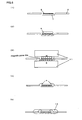
- the heat conductive adhesive A is applied with a dispenser to a ball grid array type semiconductor package 2 implemented on a PCB 1 shown in Fig. 5(1) (Fig. 5(2)).
- a radiator 4 is disposed and pressed on the upper portion of the heat conductive adhesive A as shown in Fig. 5(3), and an electronic component (Fig. 5(5)) is prepared by heat setting the heat conductive adhesive A in a magnetic field atmosphere where N pole and S pole of a permanent magnet 11 of flux density 0.6 tesla are opposed as shown in Fig. 5(4).
- the apparatus is turned on to measure the heat resistance after 6 minutes, obtaining 0.48°C/W.
- a heat conductive adhesive A similar to the Example 1 is applied with a dispenser to a ball grid array type semiconductor package 2 implemented on a PCB 1 shown in Fig. 5(1) (Fig. 5(2)).
- a radiator 4 is disposed and pressed on the upper portion of the heat conductive adhesive A as shown in Fig. 5(3), and an electronic component (Fig. 5(5)) is prepared by heat setting the heat conductive adhesive A without impressing the magnetic field.
- the apparatus is turned on to measure the heat resistance after 6 minutes, obtaining 0.61°C/W.
- a heat conductive adhesive B is prepared by blending 80 weight parts of hexagonal crystalline system flake form boron nitride powder (made by Showa Denko K.K. UHP-S1 average particle diameter 1 to 2 ⁇ m) and 100 weight parts of added type liquid silicon rubber (made by GE Toshiba silicones, TSE3331) as adhesive polymer, and degassing in a vacuum.
- the heat conductive adhesive B is applied with a dispenser to a ball grid array type semiconductor package 2 implemented on a PCB 1 shown in Fig. 5(1) (Fig. 5(2)) as in the Example 1.
- a radiator 4 is disposed and pressed on the upper portion of the heat conductive adhesive B as shown in Fig. 5(3), and an electronic component (Fig. 5(5)) is prepared by heat setting the heat conductive adhesive B in a magnetic field atmosphere where N pole and S pole of an electromagnetic magnet 11 of flux density 2 tesla are opposed as shown in Fig. 5(4).
- the apparatus is turned on to measure the heat resistance after 6 minutes, obtaining 0.37°C/W.
- a heat conductive adhesive B similar to the Example 2 is applied with a dispenser to a ball grid array type semiconductor package 2 implemented on a PCB 1 shown in Fig. 5(1) (Fig. 5(2)).
- a radiator 4 is disposed and pressed on the upper portion of the heat conductive adhesive B as shown in Fig. 5(3), and an electronic component (Fig. 5(5)) is prepared by heat setting the heat conductive adhesive B without impressing the magnetic field.
- the apparatus is turned on to measure the heat resistance after 6 minutes, obtaining 0.48°C/W.
- a heat conductive adhesive C is prepared by blending 120 weight parts of hexagonal crystalline system fine particle form boron nitride powder (made by Denki Kagaku Kogyo K.K. SP-1 average particle diameter 0.6 ⁇ m) and 100 weight parts of thermo-setting polyimide (made by Ube Industries, Ltd. Yupitite UPA-83), and degassing in a vacuum.
- the heat conductive adhesive C is screen printed on a die pad 7 of a lead frame 6 shown in Fig. 6(1) (Fig. 6(2)).
- a semiconductor chip 8 is disposed and pressed on the upper portion of the heat conductive adhesive C as shown in Fig. 6(2), and the heat conductive adhesive C is heat set in a magnetic field atmosphere where N pole and S pole of an electromagnetic magnet 11 of flux density 2 tesla are opposed as shown in Fig 6(3).
- An electronic component(Fig. 6(5)) is manufactured by connecting an electrode portion of the semiconductor chip 8 and a lead portion of the lead frame 6 by a bonding wire 9 (Fig. 6(4)) and by transfer molding with epoxy base sealant 10.
- the apparatus is turned on to measure the heat resistance after 6 minutes, obtaining 0.28°C/W.
- a heat conductive adhesive C similar to Example 3 is screen printed on a die pad 7 of a lead frame 6 shown in Fig. 6(1) (Fig. 6(1)).
- a semiconductor chip 8 is disposed and pressed on the upper portion of the heat conductive adhesive C as shown in Fig. 6(2), and the heat conductive adhesive C is heat set without impressing the magnetic field.
- An electronic component (Fig. 6(5)) is manufactured by connecting the electrode portion of the semiconductor chip 8 and the lead portion of the lead frame 6 by a bonding wire 9 (Fig. 6(4)) and by transfer molding with epoxy base sealant 10.
- the apparatus is turned on to measure the heat resistance after 6 minutes, obtaining 0.40°C/W.
- the electronic components made by the adhesion methods of Example 1 ⁇ Example 3 of the present invention are low in heat resistance value and excellent in heat conductivity because boron nitride powder is oriented by magnetic field in the heat conductive adhesive. Therefore, the adhesion method of the present invention can be applied largely to the adhesion of a semiconductor package of high heating value and a radiator such as a heat sink, or adhesion of a semiconductor chip of high heating value and a die pad portion, and supply a useful electronic component that is low in heat resistance and excellent in heat conductivity.
Landscapes
- Chemical & Material Sciences (AREA)
- Organic Chemistry (AREA)
- Inorganic Chemistry (AREA)
- Adhesives Or Adhesive Processes (AREA)
- Cooling Or The Like Of Semiconductors Or Solid State Devices (AREA)
Claims (8)
- Procédé de collage pour coller des objets à coller en interposant un adhésif conducteur de chaleur fabriqué en mélangeant de la poudre de nitrure de bore qui possède une susceptibilité magnétique anisotrope et un polymère adhésif entre lesdits objets, et en collant par orientation de la poudre de nitrure de bore dans l'adhésif conducteur de chaleur selon une direction fixée sous un champs magnétique en utilisant la susceptibilité magnétique anisotrope de la poudre de nitrure de bore.
- Procédé de collage comme revendiqué dans la revendication 1, caractérisé en ce que l'adhésif conducteur de chaleur comprend 10 à 400 parties en poids de poudre de nitrure de bore pour 100 parties en poids de polymère adhésif.
- Procédé de collage comme revendiqué dans la revendication 1 ou 2, caractérisé en ce que le polymère adhésif est au moins un type sélectionné parmi le polymère adhésif à base d'époxy, à base de polyimide, à base acrylique, à base d'uréthane et à base de silicone.
- Procédé de collage comme revendiqué dans une quelconque des revendications 1 à 3, caractérisé en ce que la poudre de nitrure de bore est en forme de flocon et le diamètre principal maximum de particule de la poudre de nitrure de bore est compris dans le domaine de 0,5 à 50 µm.
- Procédé de collage comme revendiqué dans les revendications 1 à 4, caractérisé en ce que l'adhésif conducteur de chaleur possède des propriétés d'isolant électrique.
- Composant électronique caractérisé par sa structure dans laquelle un adhésif conducteur de chaleur fabriqué en mélangeant de la poudre de nitrure de bore qui possède une susceptibilité magnétique anisotrope et un polymère adhésif est interposé entre un dispositif de chauffage et un élément conducteur de chaleur, et en collant avec de la poudre de nitrure de bore orientée dans l'adhésif conducteur de chaleur selon une direction fixée sous un champs magnétique en utilisant la susceptibilité magnétique anisotrope de la poudre de nitrure de bore.
- Composant électronique comme revendiqué dans la revendication 6, caractérisé en ce que la poudre de nitrure de bore est en forme de flocon et le diamètre principal maximum de particule de la poudre de nitrure de bore est compris dams le domaine de 0,5 à 50 µm.
- Composant électronique comme revendiqué dans la revendication 6 ou 7, caractérisé en ce que l'adhésif conducteur de chaleur possède des propriétés d'isolant électrique.
Applications Claiming Priority (2)
| Application Number | Priority Date | Filing Date | Title |
|---|---|---|---|
| JP35864799A JP4528397B2 (ja) | 1999-12-17 | 1999-12-17 | 接着方法および電子部品 |
| JP35864799 | 1999-12-17 |
Publications (4)
| Publication Number | Publication Date |
|---|---|
| EP1108766A2 EP1108766A2 (fr) | 2001-06-20 |
| EP1108766A3 EP1108766A3 (fr) | 2001-09-19 |
| EP1108766A9 EP1108766A9 (fr) | 2002-04-03 |
| EP1108766B1 true EP1108766B1 (fr) | 2004-04-07 |
Family
ID=18460401
Family Applications (1)
| Application Number | Title | Priority Date | Filing Date |
|---|---|---|---|
| EP00311186A Expired - Lifetime EP1108766B1 (fr) | 1999-12-17 | 2000-12-14 | Méthode d'adhésion et composant électronique |
Country Status (4)
| Country | Link |
|---|---|
| US (2) | US6649012B2 (fr) |
| EP (1) | EP1108766B1 (fr) |
| JP (1) | JP4528397B2 (fr) |
| DE (1) | DE60009646T2 (fr) |
Cited By (1)
| Publication number | Priority date | Publication date | Assignee | Title |
|---|---|---|---|---|
| DE102007039902A1 (de) * | 2007-08-23 | 2008-10-16 | Siemens Ag | Wärmeleitmaterial mit zwei Materialbestandteilen und Verwendung des Wärmeleitmaterials |
Families Citing this family (84)
| Publication number | Priority date | Publication date | Assignee | Title |
|---|---|---|---|---|
| JP2001172398A (ja) * | 1999-12-17 | 2001-06-26 | Polymatech Co Ltd | 熱伝導性成形体およびその製造方法 |
| JP3468420B2 (ja) * | 2000-06-07 | 2003-11-17 | 持田商工株式会社 | 放熱シート及びその製造方法 |
| WO2002084631A1 (fr) * | 2001-04-11 | 2002-10-24 | Sony Corporation | Procede de transfert d'element, procede de disposition d'element mettant en oeuvre ce procede et procede de production d'un appareil d'affichage d'image |
| DE10120928C1 (de) * | 2001-04-30 | 2002-10-31 | Infineon Technologies Ag | Verfahren zum Erstellen einer Kontaktverbindung zwischen einem Halbleiterchip und einem Substrat, insbesondere zwischen einem Speichermodulchip und einem Speichermodulboard |
| US6645612B2 (en) | 2001-08-07 | 2003-11-11 | Saint-Gobain Ceramics & Plastics, Inc. | High solids hBN slurry, hBN paste, spherical hBN powder, and methods of making and using them |
| US20030095388A1 (en) * | 2001-11-16 | 2003-05-22 | Jinbao Jiao | Method and apparatus for securing a circuit board to a rigid surface |
| US7147367B2 (en) * | 2002-06-11 | 2006-12-12 | Saint-Gobain Performance Plastics Corporation | Thermal interface material with low melting alloy |
| US7210227B2 (en) * | 2002-11-26 | 2007-05-01 | Intel Corporation | Decreasing thermal contact resistance at a material interface |
| US6916688B1 (en) * | 2002-12-05 | 2005-07-12 | National Semiconductor Corporation | Apparatus and method for a wafer level chip scale package heat sink |
| US7494635B2 (en) | 2003-08-21 | 2009-02-24 | Saint-Gobain Ceramics & Plastics, Inc. | Boron nitride agglomerated powder |
| US7180173B2 (en) * | 2003-11-20 | 2007-02-20 | Taiwan Semiconductor Manufacturing Co. Ltd. | Heat spreader ball grid array (HSBGA) design for low-k integrated circuits (IC) |
| US7145179B2 (en) * | 2004-10-12 | 2006-12-05 | Gelcore Llc | Magnetic attachment method for LED light engines |
| JP4686274B2 (ja) * | 2005-06-30 | 2011-05-25 | ポリマテック株式会社 | 放熱部品及びその製造方法 |
| US7236562B2 (en) * | 2005-11-03 | 2007-06-26 | General Electric Company | Method of assembly and thermal management of CT detector electronics circuits |
| JP2007145677A (ja) * | 2005-11-30 | 2007-06-14 | Teijin Ltd | 芳香族ポリアミドにより被覆された窒化ホウ素ナノチューブ |
| JP4922018B2 (ja) | 2007-03-06 | 2012-04-25 | 株式会社東芝 | 回転電機のコイル絶縁物 |
| DE102007045418B4 (de) * | 2007-09-21 | 2011-05-12 | Sew-Eurodrive Gmbh & Co. Kg | Herstellungsverfahren für eine Anordnung zum Kühlen eines elektrischen Bauelements |
| WO2009041974A1 (fr) * | 2007-09-27 | 2009-04-02 | Vishay Dale Electronics, Inc. | Résistance de puissance |
| US7906373B1 (en) * | 2008-03-26 | 2011-03-15 | Pawel Czubarow | Thermally enhanced electrically insulative adhesive paste |
| JP5344880B2 (ja) * | 2008-10-01 | 2013-11-20 | 三井化学株式会社 | 接着樹脂組成物、およびそれを含む積層体 |
| US10434757B2 (en) * | 2009-03-31 | 2019-10-08 | Sanofi-Aventis Deutschland Gmbh | Method of manufacturing a drug delivery device body |
| US8287996B2 (en) * | 2009-12-21 | 2012-10-16 | Intel Corporation | Coating for a microelectronic device, treatment comprising same, and method of managing a thermal profile of a microelectronic die |
| TW201203477A (en) * | 2010-01-29 | 2012-01-16 | Nitto Denko Corp | Power module |
| JP2012039064A (ja) * | 2010-01-29 | 2012-02-23 | Nitto Denko Corp | 熱伝導性シート |
| TWI513810B (zh) | 2010-01-29 | 2015-12-21 | 日東電工股份有限公司 | 攝像零件 |
| US8592844B2 (en) | 2010-01-29 | 2013-11-26 | Nitto Denko Corporation | Light-emitting diode device |
| DE102010050900A1 (de) * | 2010-11-10 | 2012-05-10 | Esk Ceramics Gmbh & Co. Kg | Bornitrid-Agglomerate, Verfahren zu deren Herstellung und deren Verwendung |
| JP2012253151A (ja) * | 2011-06-01 | 2012-12-20 | Toyota Industries Corp | 電子機器 |
| JP5619830B2 (ja) * | 2011-08-24 | 2014-11-05 | パナソニック株式会社 | 樹脂−反磁性物質複合構造体、その製造方法、およびそれを用いた半導体装置 |
| DE102012201426A1 (de) * | 2012-02-01 | 2013-08-01 | Leibniz-Institut Für Polymerforschung Dresden E.V. | Verfahren zum verbinden von kunststoffen und verfahren zum lösen einer verbindung im kunststoffverbund und kunststoffverbund |
| EP2897995B1 (fr) * | 2012-09-19 | 2019-03-20 | Momentive Performance Materials Inc. | Mélange maître comprenant du nitrure de bore, composites pulvérulents de celui-ci et compositions et articles comprenant de tels matériaux |
| US20140252566A1 (en) * | 2013-03-06 | 2014-09-11 | Rf Micro Devices, Inc. | Silicon-on-dual plastic (sodp) technology and methods of manufacturing the same |
| US9214337B2 (en) | 2013-03-06 | 2015-12-15 | Rf Micro Devices, Inc. | Patterned silicon-on-plastic (SOP) technology and methods of manufacturing the same |
| US9812350B2 (en) | 2013-03-06 | 2017-11-07 | Qorvo Us, Inc. | Method of manufacture for a silicon-on-plastic semiconductor device with interfacial adhesion layer |
| US9583414B2 (en) | 2013-10-31 | 2017-02-28 | Qorvo Us, Inc. | Silicon-on-plastic semiconductor device and method of making the same |
| US9464214B2 (en) | 2014-02-25 | 2016-10-11 | The Boeing Company | Thermally conductive flexible adhesive for aerospace applications |
| US9824951B2 (en) | 2014-09-12 | 2017-11-21 | Qorvo Us, Inc. | Printed circuit module having semiconductor device with a polymer substrate and methods of manufacturing the same |
| US10085352B2 (en) | 2014-10-01 | 2018-09-25 | Qorvo Us, Inc. | Method for manufacturing an integrated circuit package |
| US10121718B2 (en) | 2014-11-03 | 2018-11-06 | Qorvo Us, Inc. | Printed circuit module having a semiconductor device with a protective layer in place of a low-resistivity handle layer |
| US9960145B2 (en) | 2015-03-25 | 2018-05-01 | Qorvo Us, Inc. | Flip chip module with enhanced properties |
| US9613831B2 (en) | 2015-03-25 | 2017-04-04 | Qorvo Us, Inc. | Encapsulated dies with enhanced thermal performance |
| US20160343604A1 (en) | 2015-05-22 | 2016-11-24 | Rf Micro Devices, Inc. | Substrate structure with embedded layer for post-processing silicon handle elimination |
| US10276495B2 (en) | 2015-09-11 | 2019-04-30 | Qorvo Us, Inc. | Backside semiconductor die trimming |
| US10020405B2 (en) | 2016-01-19 | 2018-07-10 | Qorvo Us, Inc. | Microelectronics package with integrated sensors |
| US20170227167A1 (en) * | 2016-02-05 | 2017-08-10 | Chung-Ping Lai | Light-emitting diode filament lamp |
| US10062583B2 (en) | 2016-05-09 | 2018-08-28 | Qorvo Us, Inc. | Microelectronics package with inductive element and magnetically enhanced mold compound component |
| US10468329B2 (en) | 2016-07-18 | 2019-11-05 | Qorvo Us, Inc. | Thermally enhanced semiconductor package having field effect transistors with back-gate feature |
| US10773952B2 (en) | 2016-05-20 | 2020-09-15 | Qorvo Us, Inc. | Wafer-level package with enhanced performance |
| US10784149B2 (en) | 2016-05-20 | 2020-09-22 | Qorvo Us, Inc. | Air-cavity module with enhanced device isolation |
| US10103080B2 (en) | 2016-06-10 | 2018-10-16 | Qorvo Us, Inc. | Thermally enhanced semiconductor package with thermal additive and process for making the same |
| SG11201901193UA (en) | 2016-08-12 | 2019-03-28 | Qorvo Us Inc | Wafer-level package with enhanced performance |
| CN109716511A (zh) | 2016-08-12 | 2019-05-03 | Qorvo美国公司 | 具有增强性能的晶片级封装 |
| EP4672306A2 (fr) | 2016-08-12 | 2025-12-31 | Qorvo Us, Inc. | Procédé de fabrication d'un boîtier au niveau de la tranche avec une performance améliorée |
| US10109502B2 (en) | 2016-09-12 | 2018-10-23 | Qorvo Us, Inc. | Semiconductor package with reduced parasitic coupling effects and process for making the same |
| US10090339B2 (en) | 2016-10-21 | 2018-10-02 | Qorvo Us, Inc. | Radio frequency (RF) switch |
| US10749518B2 (en) | 2016-11-18 | 2020-08-18 | Qorvo Us, Inc. | Stacked field-effect transistor switch |
| US10068831B2 (en) | 2016-12-09 | 2018-09-04 | Qorvo Us, Inc. | Thermally enhanced semiconductor package and process for making the same |
| US10490471B2 (en) | 2017-07-06 | 2019-11-26 | Qorvo Us, Inc. | Wafer-level packaging for enhanced performance |
| US10784233B2 (en) | 2017-09-05 | 2020-09-22 | Qorvo Us, Inc. | Microelectronics package with self-aligned stacked-die assembly |
| US10366972B2 (en) | 2017-09-05 | 2019-07-30 | Qorvo Us, Inc. | Microelectronics package with self-aligned stacked-die assembly |
| US10281129B1 (en) * | 2018-01-18 | 2019-05-07 | Bgt Materials Limited | Filament structure of LED light bulb |
| US10283683B1 (en) * | 2018-01-18 | 2019-05-07 | Bgt Materials Limited | Filament structure and LED light bulb having the same |
| US11152363B2 (en) | 2018-03-28 | 2021-10-19 | Qorvo Us, Inc. | Bulk CMOS devices with enhanced performance and methods of forming the same utilizing bulk CMOS process |
| WO2019195428A1 (fr) | 2018-04-04 | 2019-10-10 | Qorvo Us, Inc. | Module à base de nitrure de gallium à performance électrique améliorée et son procédé de fabrication |
| US12046505B2 (en) | 2018-04-20 | 2024-07-23 | Qorvo Us, Inc. | RF devices with enhanced performance and methods of forming the same utilizing localized SOI formation |
| US10804246B2 (en) | 2018-06-11 | 2020-10-13 | Qorvo Us, Inc. | Microelectronics package with vertically stacked dies |
| US12165951B2 (en) | 2018-07-02 | 2024-12-10 | Qorvo Us, Inc. | RF devices with enhanced performance and methods of forming the same |
| US10964554B2 (en) | 2018-10-10 | 2021-03-30 | Qorvo Us, Inc. | Wafer-level fan-out package with enhanced performance |
| US11069590B2 (en) | 2018-10-10 | 2021-07-20 | Qorvo Us, Inc. | Wafer-level fan-out package with enhanced performance |
| US11646242B2 (en) | 2018-11-29 | 2023-05-09 | Qorvo Us, Inc. | Thermally enhanced semiconductor package with at least one heat extractor and process for making the same |
| US12057374B2 (en) | 2019-01-23 | 2024-08-06 | Qorvo Us, Inc. | RF devices with enhanced performance and methods of forming the same |
| US12125825B2 (en) | 2019-01-23 | 2024-10-22 | Qorvo Us, Inc. | RF devices with enhanced performance and methods of forming the same |
| US11387157B2 (en) | 2019-01-23 | 2022-07-12 | Qorvo Us, Inc. | RF devices with enhanced performance and methods of forming the same |
| US12046570B2 (en) | 2019-01-23 | 2024-07-23 | Qorvo Us, Inc. | RF devices with enhanced performance and methods of forming the same |
| US12046483B2 (en) | 2019-01-23 | 2024-07-23 | Qorvo Us, Inc. | RF devices with enhanced performance and methods of forming the same |
| EP3915134A1 (fr) | 2019-01-23 | 2021-12-01 | Qorvo US, Inc. | Dispositif semiconducteur radiofréquence et son procédé de fabrication |
| US12074086B2 (en) | 2019-11-01 | 2024-08-27 | Qorvo Us, Inc. | RF devices with nanotube particles for enhanced performance and methods of forming the same |
| US11646289B2 (en) | 2019-12-02 | 2023-05-09 | Qorvo Us, Inc. | RF devices with enhanced performance and methods of forming the same |
| US11923238B2 (en) | 2019-12-12 | 2024-03-05 | Qorvo Us, Inc. | Method of forming RF devices with enhanced performance including attaching a wafer to a support carrier by a bonding technique without any polymer adhesive |
| EP3835332A1 (fr) | 2019-12-13 | 2021-06-16 | Henkel AG & Co. KGaA | Composition adhésive de polyuréthane thermoconducteur |
| US12129168B2 (en) | 2019-12-23 | 2024-10-29 | Qorvo Us, Inc. | Microelectronics package with vertically stacked MEMS device and controller device |
| CN115039213A (zh) * | 2020-02-18 | 2022-09-09 | Ev 集团 E·索尔纳有限责任公司 | 用于传递构件的方法和装置 |
| CN116583949A (zh) | 2020-12-11 | 2023-08-11 | Qorvo美国公司 | 多级3d堆叠式封装和其形成方法 |
| US12062571B2 (en) | 2021-03-05 | 2024-08-13 | Qorvo Us, Inc. | Selective etching process for SiGe and doped epitaxial silicon |
Family Cites Families (12)
| Publication number | Priority date | Publication date | Assignee | Title |
|---|---|---|---|---|
| ZA741474B (en) * | 1974-03-07 | 1975-10-29 | Edenvale Eng Works | Abrasive tools |
| JPS62194653A (ja) | 1986-02-21 | 1987-08-27 | Hitachi Ltd | 半導体装置 |
| JPS6362762A (ja) | 1986-09-03 | 1988-03-19 | Hitachi Maxell Ltd | 感熱転写記録材 |
| JPH0638460B2 (ja) * | 1989-11-08 | 1994-05-18 | 東海ゴム工業株式会社 | 放熱シート |
| JPH04130175A (ja) * | 1990-09-19 | 1992-05-01 | Toray Ind Inc | エポキシ樹脂系接着剤組成物 |
| JP2915665B2 (ja) * | 1991-12-20 | 1999-07-05 | 松下電工株式会社 | 絶縁シートとそれを使った金属配線板との製造方法。 |
| CH685942A5 (fr) * | 1992-08-24 | 1995-11-15 | Battelle Memorial Institute | Procede de collage de deux substrats non metalliques a l'aide d'un adhesif. |
| JPH08245833A (ja) | 1995-01-13 | 1996-09-24 | Sumitomo Bakelite Co Ltd | 熱硬化性樹脂組成物 |
| JP3511118B2 (ja) * | 1996-08-16 | 2004-03-29 | 日立化成工業株式会社 | 接着剤、半導体装置の製造方法、および半導体装置 |
| JPH10292157A (ja) * | 1997-04-17 | 1998-11-04 | Nitto Denko Corp | 熱伝導性感圧接着シ―ト類およびこれを用いた電子部品と放熱部材との固定方法 |
| JP3434678B2 (ja) * | 1997-09-12 | 2003-08-11 | 電気化学工業株式会社 | ゴムシートの製造方法 |
| DE19841133A1 (de) | 1998-09-09 | 2000-03-16 | Abb Daimler Benz Transp | Modul einer, vorzugsweise in einem Antrieb für ein Schienenfahrzeug enthaltenen, modular aufgebauten Schaltungsanordnung |
-
1999
- 1999-12-17 JP JP35864799A patent/JP4528397B2/ja not_active Expired - Fee Related
-
2000
- 2000-12-08 US US09/733,560 patent/US6649012B2/en not_active Expired - Fee Related
- 2000-12-14 EP EP00311186A patent/EP1108766B1/fr not_active Expired - Lifetime
- 2000-12-14 DE DE60009646T patent/DE60009646T2/de not_active Expired - Lifetime
-
2003
- 2003-09-04 US US10/655,239 patent/US6918983B2/en not_active Expired - Fee Related
Cited By (1)
| Publication number | Priority date | Publication date | Assignee | Title |
|---|---|---|---|---|
| DE102007039902A1 (de) * | 2007-08-23 | 2008-10-16 | Siemens Ag | Wärmeleitmaterial mit zwei Materialbestandteilen und Verwendung des Wärmeleitmaterials |
Also Published As
| Publication number | Publication date |
|---|---|
| US20040041257A1 (en) | 2004-03-04 |
| EP1108766A9 (fr) | 2002-04-03 |
| JP2001172604A (ja) | 2001-06-26 |
| JP4528397B2 (ja) | 2010-08-18 |
| EP1108766A3 (fr) | 2001-09-19 |
| EP1108766A2 (fr) | 2001-06-20 |
| DE60009646T2 (de) | 2005-03-31 |
| US6918983B2 (en) | 2005-07-19 |
| DE60009646D1 (de) | 2004-05-13 |
| US20010004131A1 (en) | 2001-06-21 |
| US6649012B2 (en) | 2003-11-18 |
Similar Documents
| Publication | Publication Date | Title |
|---|---|---|
| EP1108766B1 (fr) | Méthode d'adhésion et composant électronique | |
| US6663969B2 (en) | Heat conductive adhesive film and manufacturing method thereof and electronic component | |
| EP1109218B1 (fr) | Moule conducteur de chaleur et procédé de sa fabrication | |
| US6660566B2 (en) | Heat conductive molded body and manufacturing method thereof and semiconductor device | |
| JP2000281995A (ja) | 熱伝導性接着フィルムおよび半導体装置 | |
| US7041535B2 (en) | Power module and method of manufacturing the same | |
| JP2000195998A (ja) | 熱伝導性シ―トおよびその製造方法ならびに半導体装置 | |
| JP2000191987A (ja) | 熱伝導性接着フィルムおよび半導体装置 | |
| JP2002088171A (ja) | 熱伝導性シートおよびその製造方法ならびに放熱装置 | |
| JP2002146672A (ja) | 熱伝導性充填剤及び熱伝導性接着剤並びに半導体装置 | |
| JP6518902B2 (ja) | 熱伝導性部材、熱伝導性組成物および熱伝導性組成物の製造方法 | |
| KR20100133449A (ko) | 열적으로 향상된 전기절연 접착용 페이스트 | |
| EP2592127A1 (fr) | Adhésif conducteur anisotrope, structure de connexion, et procédé de fabrication de ceux-ci | |
| JP2000273426A (ja) | 熱伝導性接着剤および接着方法ならびに半導体装置 | |
| JP2000191998A (ja) | 熱伝導性接着剤および接着方法ならびに半導体装置 | |
| JP2001081418A (ja) | 熱伝導性接着フィルムおよびその製造方法ならびに電子部品 | |
| JP2000348538A (ja) | 異方性導電フィルムおよびその製造方法 | |
| JP4709339B2 (ja) | 熱伝導性接着剤および接着方法ならびに電子部品 | |
| JP3991269B2 (ja) | 導電性ペースト及びそれを用いた半導体装置 | |
| JP2000022289A (ja) | 回路基板用樹脂組成物とそれを用いた回路基板 | |
| JP6394160B2 (ja) | 異方性導電接着剤、その製造方法、接続構造体及びその製造方法 | |
| JP7798080B2 (ja) | 熱伝導性部材、熱伝導性部材の製造方法、および、電池モジュール | |
| WO2006091815A2 (fr) | Composes conducteurs hautement thermique | |
| JPH02143433A (ja) | 半導体素子のダイボンディング方法 | |
| JP2007084705A (ja) | 樹脂組成物とこれを用いた回路基板およびパッケージ |
Legal Events
| Date | Code | Title | Description |
|---|---|---|---|
| PUAI | Public reference made under article 153(3) epc to a published international application that has entered the european phase |
Free format text: ORIGINAL CODE: 0009012 |
|
| AK | Designated contracting states |
Kind code of ref document: A2 Designated state(s): AT BE CH CY DE DK ES FI FR GB GR IE IT LI LU MC NL PT SE TR Kind code of ref document: A2 Designated state(s): DE GB NL |
|
| AX | Request for extension of the european patent |
Free format text: AL;LT;LV;MK;RO;SI |
|
| PUAL | Search report despatched |
Free format text: ORIGINAL CODE: 0009013 |
|
| RIC1 | Information provided on ipc code assigned before grant |
Free format text: 7C 09J 5/00 A, 7C 09J 5/06 B, 7C 09J 11/04 B, 7C 09J 9/00 B, 7C 08K 3/38 B, 7H 01L 23/373 B, 7H 01L 23/433 B, 7H 01L 21/56 B, 7H 01L 21/58 B, 7H 01L 23/495 B |
|
| AK | Designated contracting states |
Kind code of ref document: A3 Designated state(s): AT BE CH CY DE DK ES FI FR GB GR IE IT LI LU MC NL PT SE TR |
|
| AX | Request for extension of the european patent |
Free format text: AL;LT;LV;MK;RO;SI |
|
| RIN1 | Information on inventor provided before grant (corrected) |
Inventor name: YAMATO, MASAHUMI Inventor name: TOBITA, MASAYUKI Inventor name: KIMURA, TSUNEHISA Inventor name: TATEDA, SHINYA |
|
| RIN1 | Information on inventor provided before grant (corrected) |
Inventor name: TATEDA, SHINYA Inventor name: TOBITA, MASAYUKI Inventor name: YAMATO, MASAHUMI Inventor name: KIMURA, TSUNEHISA |
|
| 17P | Request for examination filed |
Effective date: 20011113 |
|
| 17Q | First examination report despatched |
Effective date: 20020228 |
|
| AKX | Designation fees paid |
Free format text: DE GB NL |
|
| GRAH | Despatch of communication of intention to grant a patent |
Free format text: ORIGINAL CODE: EPIDOS IGRA |
|
| GRAS | Grant fee paid |
Free format text: ORIGINAL CODE: EPIDOSNIGR3 |
|
| RIN1 | Information on inventor provided before grant (corrected) |
Inventor name: TOBITA, MASAYUKI Inventor name: KIMURA, TSUNEHISA Inventor name: TATEDA, SHINYA Inventor name: YAMATO, MASAHUMI |
|
| GRAA | (expected) grant |
Free format text: ORIGINAL CODE: 0009210 |
|
| AK | Designated contracting states |
Kind code of ref document: B1 Designated state(s): DE GB NL |
|
| REG | Reference to a national code |
Ref country code: GB Ref legal event code: FG4D |
|
| REF | Corresponds to: |
Ref document number: 60009646 Country of ref document: DE Date of ref document: 20040513 Kind code of ref document: P |
|
| PLBE | No opposition filed within time limit |
Free format text: ORIGINAL CODE: 0009261 |
|
| STAA | Information on the status of an ep patent application or granted ep patent |
Free format text: STATUS: NO OPPOSITION FILED WITHIN TIME LIMIT |
|
| 26N | No opposition filed |
Effective date: 20050110 |
|
| PGFP | Annual fee paid to national office [announced via postgrant information from national office to epo] |
Ref country code: NL Payment date: 20091204 Year of fee payment: 10 |
|
| PGFP | Annual fee paid to national office [announced via postgrant information from national office to epo] |
Ref country code: GB Payment date: 20101208 Year of fee payment: 11 |
|
| PGFP | Annual fee paid to national office [announced via postgrant information from national office to epo] |
Ref country code: DE Payment date: 20101208 Year of fee payment: 11 |
|
| REG | Reference to a national code |
Ref country code: NL Ref legal event code: V1 Effective date: 20110701 |
|
| PG25 | Lapsed in a contracting state [announced via postgrant information from national office to epo] |
Ref country code: NL Free format text: LAPSE BECAUSE OF NON-PAYMENT OF DUE FEES Effective date: 20110701 |
|
| GBPC | Gb: european patent ceased through non-payment of renewal fee |
Effective date: 20111214 |
|
| REG | Reference to a national code |
Ref country code: DE Ref legal event code: R119 Ref document number: 60009646 Country of ref document: DE Effective date: 20120703 |
|
| PG25 | Lapsed in a contracting state [announced via postgrant information from national office to epo] |
Ref country code: DE Free format text: LAPSE BECAUSE OF NON-PAYMENT OF DUE FEES Effective date: 20120703 Ref country code: GB Free format text: LAPSE BECAUSE OF NON-PAYMENT OF DUE FEES Effective date: 20111214 |