EP1111666A2 - Procédé de création de structures sur des circuits intégrés - Google Patents
Procédé de création de structures sur des circuits intégrés Download PDFInfo
- Publication number
- EP1111666A2 EP1111666A2 EP00890355A EP00890355A EP1111666A2 EP 1111666 A2 EP1111666 A2 EP 1111666A2 EP 00890355 A EP00890355 A EP 00890355A EP 00890355 A EP00890355 A EP 00890355A EP 1111666 A2 EP1111666 A2 EP 1111666A2
- Authority
- EP
- European Patent Office
- Prior art keywords
- masking structure
- auxiliary layer
- masking
- layer
- planarization
- Prior art date
- Legal status (The legal status is an assumption and is not a legal conclusion. Google has not performed a legal analysis and makes no representation as to the accuracy of the status listed.)
- Withdrawn
Links
Images

Classifications
-
- H—ELECTRICITY
- H10—SEMICONDUCTOR DEVICES; ELECTRIC SOLID-STATE DEVICES NOT OTHERWISE PROVIDED FOR
- H10P—GENERIC PROCESSES OR APPARATUS FOR THE MANUFACTURE OR TREATMENT OF DEVICES COVERED BY CLASS H10
- H10P50/00—Etching of wafers, substrates or parts of devices
- H10P50/73—Etching of wafers, substrates or parts of devices using masks for insulating materials
-
- H—ELECTRICITY
- H10—SEMICONDUCTOR DEVICES; ELECTRIC SOLID-STATE DEVICES NOT OTHERWISE PROVIDED FOR
- H10P—GENERIC PROCESSES OR APPARATUS FOR THE MANUFACTURE OR TREATMENT OF DEVICES COVERED BY CLASS H10
- H10P50/00—Etching of wafers, substrates or parts of devices
- H10P50/69—Etching of wafers, substrates or parts of devices using masks for semiconductor materials
- H10P50/691—Etching of wafers, substrates or parts of devices using masks for semiconductor materials for Group IV materials or Group III-V materials
- H10P50/693—Etching of wafers, substrates or parts of devices using masks for semiconductor materials for Group IV materials or Group III-V materials characterised by their size, orientation, disposition, behaviour or shape, in horizontal or vertical plane
- H10P50/695—Etching of wafers, substrates or parts of devices using masks for semiconductor materials for Group IV materials or Group III-V materials characterised by their size, orientation, disposition, behaviour or shape, in horizontal or vertical plane characterised by the process involved to create the mask, e.g. lift-off masks or sidewalls or to modify the mask
-
- H—ELECTRICITY
- H10—SEMICONDUCTOR DEVICES; ELECTRIC SOLID-STATE DEVICES NOT OTHERWISE PROVIDED FOR
- H10P—GENERIC PROCESSES OR APPARATUS FOR THE MANUFACTURE OR TREATMENT OF DEVICES COVERED BY CLASS H10
- H10P50/00—Etching of wafers, substrates or parts of devices
- H10P50/71—Etching of wafers, substrates or parts of devices using masks for conductive or resistive materials
-
- H—ELECTRICITY
- H10—SEMICONDUCTOR DEVICES; ELECTRIC SOLID-STATE DEVICES NOT OTHERWISE PROVIDED FOR
- H10P—GENERIC PROCESSES OR APPARATUS FOR THE MANUFACTURE OR TREATMENT OF DEVICES COVERED BY CLASS H10
- H10P76/00—Manufacture or treatment of masks on semiconductor bodies, e.g. by lithography or photolithography
- H10P76/40—Manufacture or treatment of masks on semiconductor bodies, e.g. by lithography or photolithography of masks comprising inorganic materials
- H10P76/408—Manufacture or treatment of masks on semiconductor bodies, e.g. by lithography or photolithography of masks comprising inorganic materials characterised by their sizes, orientations, dispositions, behaviours or shapes
- H10P76/4085—Manufacture or treatment of masks on semiconductor bodies, e.g. by lithography or photolithography of masks comprising inorganic materials characterised by their sizes, orientations, dispositions, behaviours or shapes characterised by the processes involved to create the masks
Definitions
- the invention relates to a method for producing structures in chips, in which a sequence of structuring steps self-adjusting is applied.
- each individual structuring step is hereby using a mask, each time one Photo mask must be precisely aligned.
- the photo mask exactly on the already existing structure to be aligned with whatever the structures that are becoming smaller in semiconductor production place high demands to the adjustment accuracy.
- the process flow should be kept as simple as possible to keep the manufacturing costs as low as possible.
- the present invention aims to be a simple method to create structures in chips at which aligning the photo masks and the associated Adjustment problems are avoided and which for the production of small structures.
- the Structuring steps are self-adjusting and a simple process flow can be guaranteed.
- the method according to the invention exists to achieve this object essentially in that by structuring a first auxiliary layer applied to a support after a first Masking a first masking structure is formed, which protrude at least one over the surface of the carrier Sub-area has that subsequently another Structuring step, for example by etching, implanting or CVD (chemical vapor deposition), using the previously produced first masking structure made as a mask and that then the first masking structure for training a second masking structure thereby inverted is that at least a second on the first masking structure Auxiliary layer applied, at least the structure thus formed partially removed and the resulting first auxiliary layer is selectively removed, whereupon the second masking structure as a mask for a further structuring step is used.
- subsequently another Structuring step for example by etching, implanting or CVD (chemical vapor deposition)
- a first auxiliary layer applied to a support after a a masking structure is formed for the first masking which protrude at least one over the surface of the carrier Sub-area is the prerequisite for this created one in subsequent structuring steps Inversion of the structure in such a way that the im first projecting sub-area formed is removed and remaining parts each as reference elements for the Self-adjustment take effect.
- Masking structure can be produced in that the first masking structure is inverted.
- the inversion takes place hiebei according to the invention in that the first masking structure when a second auxiliary layer is applied and subsequently carried out an at least partial removal becomes.
- the removal can in principle be carried out by planarization, such a planarization so far only for training of flat surface structures, but not, as according to the invention proposed to use for inverting a structure has been.
- planarization which, as one preferred further development corresponds, for example by a chemical-mechanical grinding process and / or etching back process can be made, a new structure after the partial Material removal of the higher parts of the chip formed, in which the first masking structure, insofar as it is still left, is again exposed and subsequently is selectively removed.
- the remaining parts of the second Auxiliary layer form a second masking structure, which as Mask is used for the further structuring steps.
- this sequence of structuring steps results in where as an essential step an inversion the structure using planarization techniques is a particularly simple procedure for training of small structures and especially for example to form a large number of semiconductor switching or Components, such as bipolar transistors, on the Surface of the chip, so that a higher component density at the same time increased precision of the respective layer boundaries can be achieved.
- the removal is preferably carried out by a chemical-mechanical grinding or by etching back.
- etchback methods for the Planarization to invert the structure is advantageous proceeded that in addition to the first masking structure to the second auxiliary layer a planarization layer from one Material is applied that has good planarization properties owns.
- the planarization layer forms in lower ones Areas a thicker layer than over the higher chip parts. Now you can etch evenly with an ideal one Etch rate for the planarization layer and the higher ones Structures, so the topography of the planarized is transferred Layer surface on the chip surface. That way ensures that the desired inversion of the structure with high precision is achieved.
- the procedure according to the invention is such that the second Auxiliary layer and possibly not the planarization layer becomes planarizing.
- a non-planarizing etching has here the preference that the material take directed and in the first place Line is vertical, such a non-planarizing Etching especially for the formation of spacers and therefore especially for the purposes of self-adjustment Advantage is. It is therefore preferred in the context of the method proceeded so that the first and / or the second A masking structure is applied, which then anisotropic to form a spacer is etched.
- the strength of the first and / or is applied to the second masking structure in consequently ensures the precision of the adjustment, since the remaining spacers a thickness towards the surface have measured, which is essentially the strength of the applied layer corresponds.
- the procedure according to the invention is such that the first Masking structure made of silicon nitride, so that in the Follow a simple removal of this layer with conventional ones Methods, for example using hot phosphoric acid.
- the second masking structure made of silicon oxide is also advantageous trained and the planarization layer from one organic polymer.
- the removal of organic polymers can by thermal processes and for example also by plasma etching take place, layers of silicon oxide or polycrystalline Silicon in such a selective removal step cannot be changed.
- the second auxiliary layer can advantageously also consist of an organic one Polymer exist, in which case the selective Removal of this planarization layer from the rest Layers is also guaranteed.
- a carrier material that does not have any etching selectivity compared to layers to be applied subsequently has, is advantageously carried out so that the carrier itself a third auxiliary layer is made of a material with good Etching selectivity to the first and second masking structure consists.
- the deposition of the respective layers can be done with conventional Procedure.
- a second auxiliary layer is advantageous applied by means of a CVD process, the second auxiliary layer also consist of an organic polymer can, which is applied with a spin process.
- the method according to the invention is preferably suitable for Formation of bipolar transistors, due to the high Precision the electrical parameters of the transistor more precise can be adjusted.
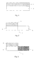
- Fig. 1 denotes a semiconductor substrate on which a first auxiliary layer 2 is applied.
- the first auxiliary layer 2 now becomes a first masking structure 3 formed, which a region 4 of the semiconductor substrate 1 covered and a further region 5 of the semiconductor substrate 1 leaves uncovered, as shown in Fig. 2 is.
- the unmasked area 5 can subsequently, for example by implantation, can be structured as shown in FIG. 3 is.
- the first masking structure 3 must be the rest In this case, the chip superstructures protrude so far that the following one Planarization step specifically removed these structures can be. 4 shows how the inversion of the masking structure 3 is being prepared.
- a second Auxiliary layer 6 on the first masking structure 3 and on the applied unmasked area 5 of the semiconductor substrate 1, whereupon all of the material towering above level 7 through planarization processes is removed.
- the exposed masking structure 3 can now, for example, by Etching, selectively removed, leaving only the second Auxiliary layer 6 remains, which is the inverted structure of the Masking 3 corresponds and as a masking structure for a subsequent structuring of area 4 of the semiconductor substrate 1 serves.
- 7 to 11 is the application of the invention Process shown on the manufacture of a bipolar transistor.
- the problem with bipolar transistors is that an intrinsic Base area and an emitter area centrally structured must become. Laterally this central area must be observed a defined distance, the base supply line structures (e.g. through an implant step or through the Growing a silicide). These two structuring steps must be exactly aligned with each other. Too big Distance means that the resistance of the base lead increases too small a distance or an overlap has the consequence that the base region is partially highly doped or that the Shorted emitter.
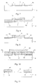
- 7 is the semiconductor substrate, in which the collector is already included, designated 8.
- the intrinsic base area should now be in area 9 and to the side of it, each observing one Distance a, extrinsic areas 10 for the base lead be formed.
- a first masking structure is used 11 applied, which is the intrinsic base area covers, as shown in Fig. 8.
- the Thickness exactly the distance a between intrinsic and extrinsic Base corresponds.
- spacer layer 12 spacers 13 are formed so that now how 9, the extrinsic areas, for example can be doped with boron.
- an auxiliary layer 14 on the first masking structure 11 Spacers and over the exposed substrate surface applied, so that now the structure shown in Fig. 10 is formed.
- the material that is outstanding over level 15 is through Planarization process removed, so that the masking structure 11 is exposed, whereupon it is removed by selective etching becomes.
Landscapes
- Bipolar Transistors (AREA)
- Drying Of Semiconductors (AREA)
Applications Claiming Priority (2)
| Application Number | Priority Date | Filing Date | Title |
|---|---|---|---|
| AT84199U | 1999-12-03 | ||
| AT0084199U AT4149U1 (de) | 1999-12-03 | 1999-12-03 | Verfahren zum herstellen von strukturen in chips |
Publications (2)
| Publication Number | Publication Date |
|---|---|
| EP1111666A2 true EP1111666A2 (fr) | 2001-06-27 |
| EP1111666A3 EP1111666A3 (fr) | 2002-12-18 |
Family
ID=3501012
Family Applications (1)
| Application Number | Title | Priority Date | Filing Date |
|---|---|---|---|
| EP00890355A Withdrawn EP1111666A3 (fr) | 1999-12-03 | 2000-11-29 | Procédé de création de structures sur des circuits intégrés |
Country Status (3)
| Country | Link |
|---|---|
| US (1) | US6562547B2 (fr) |
| EP (1) | EP1111666A3 (fr) |
| AT (1) | AT4149U1 (fr) |
Families Citing this family (1)
| Publication number | Priority date | Publication date | Assignee | Title |
|---|---|---|---|---|
| US6780736B1 (en) * | 2003-06-20 | 2004-08-24 | International Business Machines Corporation | Method for image reversal of implant resist using a single photolithography exposure and structures formed thereby |
Family Cites Families (18)
| Publication number | Priority date | Publication date | Assignee | Title |
|---|---|---|---|---|
| US3837856A (en) * | 1967-04-04 | 1974-09-24 | Signetics Corp | Method for removing photoresist in manufacture of semiconductor devices |
| US4758528A (en) * | 1980-07-08 | 1988-07-19 | International Business Machines Corporation | Self-aligned metal process for integrated circuit metallization |
| DE3124572A1 (de) | 1981-06-23 | 1982-12-30 | Siemens AG, 1000 Berlin und 8000 München | Verfahren zur herstellung von schottky-dioden |
| DE3304588A1 (de) | 1983-02-10 | 1984-08-16 | Siemens AG, 1000 Berlin und 8000 München | Verfahren zum herstellen von mos-transistoren mit flachen source/drain-gebieten, kurzen kanallaengen und einer selbstjustierten, aus einem metallsilizid bestehenden kontaktierungsebene |
| DE3330895A1 (de) | 1983-08-26 | 1985-03-14 | Siemens AG, 1000 Berlin und 8000 München | Verfahren zum herstellen von bipolartransistorstrukturen mit selbstjustierten emitter- und basisbereichen fuer hoechstfrequenzschaltungen |
| GB2172744B (en) * | 1985-03-23 | 1989-07-19 | Stc Plc | Semiconductor devices |
| US4755476A (en) | 1985-12-17 | 1988-07-05 | Siemens Aktiengesellschaft | Process for the production of self-adjusted bipolar transistor structures having a reduced extrinsic base resistance |
| US4871684A (en) * | 1987-10-29 | 1989-10-03 | International Business Machines Corporation | Self-aligned polysilicon emitter and contact structure for high performance bipolar transistors |
| US5306649A (en) * | 1991-07-26 | 1994-04-26 | Avantek, Inc. | Method for producing a fully walled emitter-base structure in a bipolar transistor |
| US5266505A (en) * | 1992-12-22 | 1993-11-30 | International Business Machines Corporation | Image reversal process for self-aligned implants in planar epitaxial-base bipolar transistors |
| JPH07142504A (ja) | 1993-11-19 | 1995-06-02 | Oki Electric Ind Co Ltd | バイポーラ型半導体集積回路装置及びその製造方法 |
| JPH07221321A (ja) | 1994-02-08 | 1995-08-18 | Nippondenso Co Ltd | 半導体装置およびその製造方法 |
| US5447874A (en) * | 1994-07-29 | 1995-09-05 | Grivna; Gordon | Method for making a semiconductor device comprising a dual metal gate using a chemical mechanical polish |
| US5614430A (en) * | 1996-03-11 | 1997-03-25 | Taiwan Semiconductor Manufacturing Company Ltd. | Anti-punchthrough ion implantation for sub-half micron channel length MOSFET devices |
| DE19609933A1 (de) * | 1996-03-14 | 1997-09-18 | Daimler Benz Ag | Verfahren zur Herstellung eines Heterobipolartransistors |
| JPH1012871A (ja) | 1996-06-21 | 1998-01-16 | Toshiba Corp | 半導体装置の製造方法 |
| US5798568A (en) * | 1996-08-26 | 1998-08-25 | Motorola, Inc. | Semiconductor component with multi-level interconnect system and method of manufacture |
| US5856225A (en) * | 1997-11-24 | 1999-01-05 | Chartered Semiconductor Manufacturing Ltd | Creation of a self-aligned, ion implanted channel region, after source and drain formation |
-
1999
- 1999-12-03 AT AT0084199U patent/AT4149U1/de not_active IP Right Cessation
-
2000
- 2000-11-29 EP EP00890355A patent/EP1111666A3/fr not_active Withdrawn
- 2000-12-01 US US09/727,389 patent/US6562547B2/en not_active Expired - Lifetime
Also Published As
| Publication number | Publication date |
|---|---|
| EP1111666A3 (fr) | 2002-12-18 |
| US20030044723A1 (en) | 2003-03-06 |
| AT4149U1 (de) | 2001-02-26 |
| US6562547B2 (en) | 2003-05-13 |
Similar Documents
| Publication | Publication Date | Title |
|---|---|---|
| EP0013317B1 (fr) | Procédé de fabrication de transistors à effet de champ | |
| DE19820223C1 (de) | Verfahren zum Herstellen einer Epitaxieschicht mit lateral veränderlicher Dotierung | |
| DE10214066B4 (de) | Halbleiterbauelement mit retrogradem Dotierprofil in einem Kanalgebiet und Verfahren zur Herstellung desselben | |
| DE19527131B4 (de) | Halbleitervorrichtung mit einer T-förmigen Gatestruktur und Verfahren zu deren Herstellung | |
| EP0021147B1 (fr) | Procédé pour la fabrication de fossés d'isolation larges et profonds dans un substrat semiconducteur | |
| DE10308870B4 (de) | Bipolartransistor mit verbessertem Basis-Emitter-Übergang und Verfahren zur Herstellung | |
| EP0020998B1 (fr) | Procédé de fabrication d'un transistor bipolaire comprenant une zône d'émetteur à implantation ionique | |
| DE2926874A1 (de) | Verfahren zum herstellen von niederohmigen, diffundierten bereichen bei der silizium-gate-technologie | |
| DE10351008B4 (de) | Verfahren zur Herstellung von Transistoren mit erhöhten Drain- und Sourcegebieten mit unterschiedlicher Höhe sowie ein Halbleiterbauelement | |
| EP0005185A1 (fr) | Procédé pour la formation simultanée de diodes à barrage Schottky et de contacts ohmiques sur des régions semi-conductrices dopées | |
| EP0684639A1 (fr) | Procédé de fabrication d'un transistor bipolaire | |
| EP0006510A1 (fr) | Procédé de formation de régions adjacentes et dopées différemment dans un substrat de silicium | |
| DE3540422C2 (de) | Verfahren zum Herstellen integrierter Strukturen mit nicht-flüchtigen Speicherzellen, die selbst-ausgerichtete Siliciumschichten und dazugehörige Transistoren aufweisen | |
| DE2128884A1 (de) | Verfahren zum Herstellen von Halbleiterbauteilen | |
| DE2849373A1 (de) | Verfahren zur herstellung einer halbleitervorrichtung | |
| DE102015204411B4 (de) | Transistor und Verfahren zur Herstellung eines Transistors | |
| DE10162074B4 (de) | BiCMOS-Struktur, Verfahren zu ihrer Herstellung und Bipolartransistor für eine BiCMOS-Struktur | |
| WO2001041205A1 (fr) | Procede de fabrication d'un transistor bipolaire et procede de fabrication d'un circuit integre comportant un tel transistor bipolaire | |
| DE69509698T2 (de) | Verfahren zur Herstellung eines Feldeffekttransistors mit isoliertem Gate und kurzem Kanal, und entsprechender Transistor | |
| DE2429957A1 (de) | Verfahren zur herstellung einer dotierten zone eines leitfaehigkeitstyps in einem halbleiterkoerper | |
| DE3883459T2 (de) | Verfahren zum Herstellen komplementärer kontaktloser vertikaler Bipolartransistoren. | |
| DE2930780C2 (de) | Verfahren zur Herstellung eines VMOS-Transistors | |
| AT4149U1 (de) | Verfahren zum herstellen von strukturen in chips | |
| DE69901752T2 (de) | Methode zur Herstellung eines Bipolartransistors mit Eigenschaften zur Unterdrückung der Verschlechterung von Transistor-Charakteristiken | |
| WO2003049192A1 (fr) | Transistor bipolaire et procédé de fabrication associé |
Legal Events
| Date | Code | Title | Description |
|---|---|---|---|
| PUAI | Public reference made under article 153(3) epc to a published international application that has entered the european phase |
Free format text: ORIGINAL CODE: 0009012 |
|
| AK | Designated contracting states |
Kind code of ref document: A2 Designated state(s): AT BE CH CY DE DK ES FI FR GB GR IE IT LI LU MC NL PT SE TR |
|
| AX | Request for extension of the european patent |
Free format text: AL;LT;LV;MK;RO;SI |
|
| PUAL | Search report despatched |
Free format text: ORIGINAL CODE: 0009013 |
|
| AK | Designated contracting states |
Kind code of ref document: A3 Designated state(s): AT BE CH CY DE DK ES FI FR GB GR IE IT LI LU MC NL PT SE TR |
|
| AX | Request for extension of the european patent |
Free format text: AL;LT;LV;MK;RO;SI |
|
| 17P | Request for examination filed |
Effective date: 20030227 |
|
| 17Q | First examination report despatched |
Effective date: 20030401 |
|
| AKX | Designation fees paid |
Designated state(s): DE FR GB |
|
| STAA | Information on the status of an ep patent application or granted ep patent |
Free format text: STATUS: THE APPLICATION IS DEEMED TO BE WITHDRAWN |
|
| 18D | Application deemed to be withdrawn |
Effective date: 20030812 |