EP1115104A1 - Processeur d'images et affichage d'images - Google Patents
Processeur d'images et affichage d'images Download PDFInfo
- Publication number
- EP1115104A1 EP1115104A1 EP00927788A EP00927788A EP1115104A1 EP 1115104 A1 EP1115104 A1 EP 1115104A1 EP 00927788 A EP00927788 A EP 00927788A EP 00927788 A EP00927788 A EP 00927788A EP 1115104 A1 EP1115104 A1 EP 1115104A1
- Authority
- EP
- European Patent Office
- Prior art keywords
- image
- image processing
- operation mode
- section
- processing
- Prior art date
- Legal status (The legal status is an assumption and is not a legal conclusion. Google has not performed a legal analysis and makes no representation as to the accuracy of the status listed.)
- Withdrawn
Links
Images



Classifications
-
- G—PHYSICS
- G09—EDUCATION; CRYPTOGRAPHY; DISPLAY; ADVERTISING; SEALS
- G09G—ARRANGEMENTS OR CIRCUITS FOR CONTROL OF INDICATING DEVICES USING STATIC MEANS TO PRESENT VARIABLE INFORMATION
- G09G5/00—Control arrangements or circuits for visual indicators common to cathode-ray tube indicators and other visual indicators
-
- G—PHYSICS
- G09—EDUCATION; CRYPTOGRAPHY; DISPLAY; ADVERTISING; SEALS
- G09G—ARRANGEMENTS OR CIRCUITS FOR CONTROL OF INDICATING DEVICES USING STATIC MEANS TO PRESENT VARIABLE INFORMATION
- G09G3/00—Control arrangements or circuits, of interest only in connection with visual indicators other than cathode-ray tubes
- G09G3/20—Control arrangements or circuits, of interest only in connection with visual indicators other than cathode-ray tubes for presentation of an assembly of a number of characters, e.g. a page, by composing the assembly by combination of individual elements arranged in a matrix no fixed position being assigned to or needed to be assigned to the individual characters or partial characters
-
- G—PHYSICS
- G06—COMPUTING OR CALCULATING; COUNTING
- G06T—IMAGE DATA PROCESSING OR GENERATION, IN GENERAL
- G06T1/00—General purpose image data processing
- G06T1/20—Processor architectures; Processor configuration, e.g. pipelining
-
- G—PHYSICS
- G09—EDUCATION; CRYPTOGRAPHY; DISPLAY; ADVERTISING; SEALS
- G09G—ARRANGEMENTS OR CIRCUITS FOR CONTROL OF INDICATING DEVICES USING STATIC MEANS TO PRESENT VARIABLE INFORMATION
- G09G3/00—Control arrangements or circuits, of interest only in connection with visual indicators other than cathode-ray tubes
- G09G3/20—Control arrangements or circuits, of interest only in connection with visual indicators other than cathode-ray tubes for presentation of an assembly of a number of characters, e.g. a page, by composing the assembly by combination of individual elements arranged in a matrix no fixed position being assigned to or needed to be assigned to the individual characters or partial characters
- G09G3/34—Control arrangements or circuits, of interest only in connection with visual indicators other than cathode-ray tubes for presentation of an assembly of a number of characters, e.g. a page, by composing the assembly by combination of individual elements arranged in a matrix no fixed position being assigned to or needed to be assigned to the individual characters or partial characters by control of light from an independent source
- G09G3/36—Control arrangements or circuits, of interest only in connection with visual indicators other than cathode-ray tubes for presentation of an assembly of a number of characters, e.g. a page, by composing the assembly by combination of individual elements arranged in a matrix no fixed position being assigned to or needed to be assigned to the individual characters or partial characters by control of light from an independent source using liquid crystals
- G09G3/3611—Control of matrices with row and column drivers
-
- G—PHYSICS
- G09—EDUCATION; CRYPTOGRAPHY; DISPLAY; ADVERTISING; SEALS
- G09G—ARRANGEMENTS OR CIRCUITS FOR CONTROL OF INDICATING DEVICES USING STATIC MEANS TO PRESENT VARIABLE INFORMATION
- G09G2340/00—Aspects of display data processing
- G09G2340/10—Mixing of images, i.e. displayed pixel being the result of an operation, e.g. adding, on the corresponding input pixels
-
- G—PHYSICS
- G09—EDUCATION; CRYPTOGRAPHY; DISPLAY; ADVERTISING; SEALS
- G09G—ARRANGEMENTS OR CIRCUITS FOR CONTROL OF INDICATING DEVICES USING STATIC MEANS TO PRESENT VARIABLE INFORMATION
- G09G2340/00—Aspects of display data processing
- G09G2340/12—Overlay of images, i.e. displayed pixel being the result of switching between the corresponding input pixels
-
- G—PHYSICS
- G09—EDUCATION; CRYPTOGRAPHY; DISPLAY; ADVERTISING; SEALS
- G09G—ARRANGEMENTS OR CIRCUITS FOR CONTROL OF INDICATING DEVICES USING STATIC MEANS TO PRESENT VARIABLE INFORMATION
- G09G2352/00—Parallel handling of streams of display data
-
- G—PHYSICS
- G09—EDUCATION; CRYPTOGRAPHY; DISPLAY; ADVERTISING; SEALS
- G09G—ARRANGEMENTS OR CIRCUITS FOR CONTROL OF INDICATING DEVICES USING STATIC MEANS TO PRESENT VARIABLE INFORMATION
- G09G2360/00—Aspects of the architecture of display systems
- G09G2360/12—Frame memory handling
Definitions
- the present invention relates to an image-processing apparatus and an image-displaying apparatus using the same.
- the electronic apparatuses include, for example, direct-view-type displaying apparatuses and projection-type displaying apparatuses. Generally, these electronic apparatuses are configured by combining a plurality of image processing sections that individually control different functions.
- a method for improving the processing speeds is such that pieces of image data that are processed sequentially in units of one pixel are grouped in parallel corresponding to a plurality of the pixels for processing.
- image-processing sections used in an electronic apparatus include those that do not have functions for performing parallel processing for a plurality of pixels.
- an arrangement is made such that a plurality of image processing sections having the same functions is provided in parallel, and image data for one pixel is processed by each of the image processing sections with the same timing. This method allows processing to be performed in parallel for image data for a plurality of pixels.
- the present invention is made to solve the problem described in the Background Art, and an object thereof is to provide techniques such that, even in a case where a plurality of image processing sections having the same functions is provided in parallel, control performed by one control unit for processing in one of the image processing sections allows processing in other image processing sections to be concurrently controlled.
- an image-processing apparatus is characterized by including n image processing sections which receive n (n represents an integer equal to or larger than "2") consecutive pixel data items that are respectively input with the same timing and which respectively process the respective input pixel data items with the same timing; and a control section for controlling the n image processing sections, wherein each of the image processing sections is capable of being set to one of a first operation mode allowing data communication with the controlling section and a second operation mode allowing only reception from the aforementioned controlling section, one of the image processing sections is set to the first operation mode, and n-1 image processing sections are set to the second operation mode; commands are commonly given to the n image processing sections from the controlling section; and when a command is given from the controlling section to the one of the image processing sections that is set to the first operation mode, the n image processing sections respectively execute the same processing with the same timing.
- the command is given from the control section to the image processing section set to the first operation mode
- the command is also given to other image processing sections that are set to the second operation mode; and thereby, the image-processing apparatus of the present invention can control processing performed by other image processing sections. That is, even in a case where a plurality of image processing sections each having the same function are provided in parallel, when one controlling section controls processing performed by one of the image processing sections, processing performed by other image processing sections can concurrently be controlled.
- the n image processing sections be allocated in the same address space in address spaces that can be controlled by the controlling section.
- the command when a command is given by the controlling section to the image processing section set to the first operation mode, the command can be given to other image processing sections set to the second operation mode.
- each of the image processing sections comprises a mode-setting terminal for setting one of the first operation mode and the second operation mode, and one of the operation modes is set according to a mode-setting signal input to the mode-setting terminal.
- the above image-processing apparatus may comprise a memory for storing image-processing data commonly used by the respective image processing sections, wherein the image processing section set to the first operation mode can write the image-processing data, which is fed from the controlling section, to the memory, and in addition, can read out the image-processing data written in the memory; and the image processing section set to the second operation mode can input the image-processing data read out by the image processing section set to the first operation mode from the memory.
- the image-processing data is written to the memory by the image processing section set to the first operation mode, and the image-processing data read out by the image processing section, which is set to the first operation mode, from the memory can be input to all the image processing sections.
- An image-displaying apparatus can be configured of the image-processing apparatus and an image-displaying section for displaying images represented by video signals output from the image-processing apparatus.
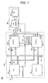
- FIG. 1 is a block diagram showing an outline configuration of an image-displaying apparatus to which an image-processing apparatus as a first embodiment of the present invention is applied.
- An image-displaying apparatus 1000 comprises an image-processing apparatus 100 and an image-displaying section 200.
- the image-processing apparatus 100 is a computer system that includes a scan converter 110 (which is simply referred to as an "SC”, hereinbelow), two on-screen display controllers 120A and 120B (each of which is simply referred to as an "OSDC”, hereinbelow), an OSD memory 130, and a CPU 140.
- the image-displaying section 200 includes a liquid crystal panel 210 and a panel-driving section 220.
- the image-processing apparatus 100 processes images to be formed on the liquid crystal panel 210. In the above, a configuration may be such that the panel-driving section 220 is provided in the image-processing apparatus 100.
- the CPU 140 is connected to the SC 110 and the two OSDCs 120A and 120B via a CPU bus 142.
- the CPU 160 sets processing conditions of respective sections and directly controls processing performed in the respective sections.
- the OSD memory 130 is connected to the first and second OSDCs 120A and 120B via a memory bus 132.
- the SC 110 outputs vertically-synchronous signals VD, horizontally-synchronous signals HD, and clock signals DCLK that are used to display images on the image-displaying section 200.
- it outputs input-video signals VS to the image-displaying section 200 as video signals DS that can be input to the image-displaying section 200.
- Image data that is output as the video signals DS has a data width of 48 bits. Specifically, image data of 24 bits per pixel is concurrently output for two consecutive pixels. The image data for one pixel is made of 8-bit color data for each of the colors red, green, and blue.
- Video signals DSD for the lower 24 bits are input to the first OSDC 120A, whereas video signals DSU for the upper 24 bits are input to the second OSDC 120B.
- Image data included in the video signals DS may be referred to as the image data DS for the convenience of description.
- Image data DSD for the lower 24 bits corresponds to odd-number-pixel image data
- image data DSU for the upper 24 bits corresponds to even-number-pixel image data.
- the above may be reverse.
- the first and second OSDCs 120A and 120B are image processing sections each having a function for displaying embellishment images, such as pointer images, and menu screens in images that are displayed in the image-displaying section 200. These first and second OSDCs 120A and 120B correspond to the image processing sections of the present invention.
- graphic data and font data that compose image data for pointer images and menu screens are stored in predetermined formats.
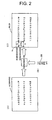
- FIG. 2 is an explanatory drawing illustrating processing to be performed by the first and second OSDCs 120A and 120B.
- the first OSDC 120A expands the image data read out from the OSD memory 130 so as to be bitmap data, and OSD image data DOD as shown in FIG. 2 (B) is thereby generated.
- the OSD image data DOD thus generated is combined with the odd-number-pixel image data DSD included in image data DS as shown in FIG. 2(A), and combined odd-number-pixel image data DSODD is thereby output.
- the second OSDC 120B also operates with the same timing as in the case of the first OSDC 120A in synchronization with the vertically-synchronous signal VD, the horizontally-synchronous signal HD, and the clock signal DCLK.
- the image data read out from the OSD memory 130 is expanded so as to be bitmap data, and OSD image data DOD as shown in FIG. 2(B) is thereby generated.
- the OSD image data DOD thus generated is combined with the even-number-pixel image data DSU included in the image data DS shown in FIG. 2(A), and combined even-number-pixel image data DSODU is thereby output.
- the 24-bit combined image data DSODD and DSODU that have been output from the first and second OSDCs 120A and 120B, respectively, is fed as 48-bit display image data DSLCD to the panel-driving section 220 shown in FIG. 1.
- the vertically-synchronous signals VD, the horizontally-synchronous signals HD, and the clock signals DCLK that are output from the SC 110 are also fed to the panel-driving section 220.
- the liquid crystal panel 210 displays an image corresponding to the aforementioned display image data DSLCD. According to the above, as shown in FIG. 2 (C), an OSD image is displayed in a position P0.
- OSD images such as menu screens and embellishment images, generated by the first and second OSCDs 120, can be combined with an input image, and the combined images can thereby be displayed.
- FIG. 3 is an outline block diagram showing an interior configuration of the first OSDC 120A.
- the first OSDC 120A includes a combination control section 310, a combining section 320, an OSD-image-generating section 330, a memory control section 340, a CPU I/F section 350, a memory I/F section 360, and a mode control section 370.
- the CPU I/F section 350 is connected to a CPU address bus ADR, a CPU data bus DTA, and a CPU control bus CTL that constitute the CPU bus 142 (FIG. 1).
- the memory I/F section 360 is connected to a memory address bus MADR, a memory data bus MDTA, and a memory control bus MCTL that constitute the memory bus 132 of the OSD memory 130 (FIG. 1).
- a master/slave-setting terminal M/S of the mode control section 370 is set to an H level, and an operation mode of the first OSDC 120A is thereby set to a master mode.
- the mode control section 370 outputs mode control signals MSC corresponding to the master mode, and thereby controls input/output conditions for the CPU I/F section 350 and the memory I/F section 360.
- the CPU I/F section 350 is controlled so as to permit input access and/or output access to the data bus DTA.
- the memory I/F section 360 is controlled so as to permit address data and control data to be output to the memory address bus MADR and the memory control bus MCTL, respectively, and so as to permit writing access and/or reading access to the OSD memory 130.
- combination control data representing the display position P0 of the OSD image (refer to FIG. 2) is set by the CPU 140 via the CPU I/F section 350. Also, the vertically-synchronous signals VD, the horizontally-synchronous signals HD, and the clock signals DCLK are input therein.
- the combination control section 310 controls the memory control section 340, the OSD-image-generating section 330, and the combining section 320 according to the combination control data, the synchronous signals HD and VD, and the clock signals DCLK that have been set.
- the memory control section 340 controls writing to the OSD memory 130 and reading therefrom via the memory I/F section 360. Also, according to a control signal output from the combination control section 310, via the memory I/F section 360, the memory control section 340 controls reading of image-processing data from the OSD memory 130, image-processing data being used when the OSD-image-generating section 330 generates OSD image data DOD.
- the OSD-image-generating section 330 outputs 24-bit OSD image data DOD according to image-processing data read out by the memory control section 340 from the OSD memory 130.
- the combining section 320 combines the odd-number-pixel image data DSD output from the SC 110 with the OSD image data DOD, and thereby generates combined odd-number-pixel image data DSODD.
- FIG. 4 is an outline block diagram showing an interior configuration of the second OSDC 120B.
- the second OSDC 120B is the same as the first OSDC 120A except that the master/slave-setting terminal M/S of the mode control section 370 is set to an L level, and the operation mode is set to a slave mode.
- the CPU I/F section 350 is controlled so as to be inhibited from outputting data to a data bus DTA and so as to be permitted only to receive data therefrom.
- the mode control section 370 is controlled so as to be inhibited from output individual data to a memory address bus MADR, a memory data bus MDTA, and a memory control bus MCTL.
- a memory control section 340 is set with the same control data as in the case of the memory control section 340 in the first OSDC 120A, it operates with the same timing as in the master mode. Therefore, the second OSDC 120B operating in the slave mode can concurrently retrieve the image-processing data that the first OSDC 120A operating in the master mode has read out from the OSD memory 130.
- FIG. 5 is an explanatory drawing showing operation performed among the first and second OSDCs 120A and 120B and the CPU 140.
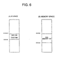
- FIG. 6 is an explanatory drawing showing an I/O address space and a memory space in the CPU 140.
- FIG. 6(A) only an address space for a single OSDC is allocated in the I/O address space in the CPU 140, and the same I/O address is allocated for the two OSDCs 120A and 120B.
- the first and second OSDCs 120A and 120B have completely the same internal functions except that the different operation modes are set. Therefore, when the CPU 140 requests the first OSDC 120A to input (write) data, as shown in FIG. 5(A), the data is input to the first OSDC 120A, and concurrently, the same data is input to the second OSDC 120B from the CPU 140 via the CPU bus 142 (the CPU address bus ADR, the CPU data bus, and the CPU control bus CTL).
- the CPU 140 requests the first OSDC 120A to write image-processing data to the OSD memory 130
- the data is input to both the first and second OSDCs 120A and 120B.
- the second OSDC 120B set to the slave mode is inhibited from outputting the data to the OSD memory 130
- writing of the data to the OSD memory 130 is executed only by the first OSDC 120A set to the master mode.
- the CPU 140 requests the first OSDC 120A to output (read) data, as described above, since the second OSDC 120B set to the slave mode is inhibited from outputting data to the CPU 140, as described in FIG. 5(B), the data is output only from the first OSDC 120A set to the master mode.
- the CPU 140 issues a request thereto for reading of image-processing data written in the OSD memory 130
- image-processing data read from the OSD memory 130 can be input to both the first and second OSDCs 120A and 120B.
- output of the data to the CPU 140 is executed only by the first OSDC 120A.
- the memory control section 340 in the second OSDC 120B set to the slave mode may be controlled so as to stop its operation.
- FIG. 7 is an explanatory drawing showing operation that is performed to display the OSD images generated by the first and second OSDCs 120A and 120B.
- the OSD image data DOD generated in the OSD-image-generating section 330 according to the image-processing data read out from the OSD memory 130 is combined with the image data DSD in the combining section 320 (FIG. 3). Therefore, combined odd-number-pixel image data DSODD is output from the first OSDC 120A.
- the second OSDC 120B image data read by the first OSDC 120A is concurrently retrieved, and even-number-pixel image data DSODU is output in the same way as that in the first OSDC 120A.
- the image data DS output from the SC 110 is combined with OSD image data DOD in the first and second OSDCs 120A and 120B with the same timing on the basis of the odd-numbered pixel and the even-numbered pixel. Accordingly, the image data for the two continuous pixels is processed in parallel and is thereby output as the display image data DSLCD.
- each of the first and second OSDCs 120A and 120B can be operated in one of the master mode and the slave mode.
- the CPU 140 issues a request for input and/or output of data to the first OSDC 120A set to the master mode
- the same data can be output to the second OSDC 120B set to the slave mode. That is, while the two first and second OSDCs 120A and 120B operate with the same timing, the CPU 140 controls the first OSDC 120A operating in the master mode, thereby allowing the second OSDC 120B operating in the slave mode to be concurrently controlled.
- the OSD image data to be generated in the OSD-image-generating section 330 is preferably generated as follows.
- the odd-number-pixel image data DSD is combined with the OSD image data DOD as shown in FIG. 2(B) in the first OSDC 120A, and concurrently, the even-number-pixel image data DSU is combined with the OSD image data DOD in the second OSDC 120B, thereby generating the display image data DSLCD that represents pixels as shown in FIG. 2(C).
- pieces of the OSD image data DOD generated with the same timing in the individual first and second OSDCs 120A and 120B are the same data.
- the OSD image data to be combined with both, the odd-number-pixel image data and the even-number-pixel image data is preferably data that has m/2 of pixels in the horizontal direction, as shown in FIG. 2(B).
- the OSD memory 130 is shared such that reading and/or writing access to the OSD memory 130 is controlled by the first OSDC 120A set to the master mode, and only the data read out by the first OSDC 120A is permitted to be used in the second OSDC 120B set to the slave mode.
- the OSD memory 130 may be provided in each of the first and second OSDCs 120A and 120B. In this case, an arrangement may be such that control in the slave mode for the memory I/F section 360 in the second OSDC 120B is cancelled, and control is then executed by the memory control section 340 for writing access and/or reading access to the OSD memory 130 connected to the second OSDC 120B. As a result, writing and/or reading of data is executed by the individual first and second OSDCs 120A and 120B with the same timing for the individual OSD memories 130.
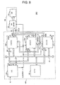
- FIG. 8 is a block diagram showing an outline configuration of an image-displaying apparatus to which an image-processing apparatus as a second embodiment of the present invention is applied.
- An image-displaying apparatus 2000 includes an image-processing apparatus 100A with three OSDCs 120A, 120B, and 120C.
- An SC 110A outputs 72-bit image data DS including image data for three consecutive pixels, and individual items of the output image data are input to the three 120A, 120B, and 120C in the unit of one pixel.
- the first OSDC 120A is set to the master mode
- the second and third OSDCs 120B and 120C are set to the slave mode.
- a CPU 140 requests the first OSDC 120A, which is set to the master mode, to input and/or output data
- the same data can be output to the second and third OSDCs 120B and 120C, which are set to the slave mode. That is, among the OSDCs 120A, 120B, and 120C that operate with the same timing, the CPU 140 controls the first OSDC 120A that operates in the master mode, thereby allowing the second and third OSDCs 120B and 120C, which operate in the slave mode, to be concurrently controlled.
- OSD image data that is combined in each of the three 120A, 120B, and 120C when image data to be displayed represents m pixels in the horizontal direction, the image data preferably represents m/3 of the pixels in the horizontal direction.
- an arrangement may be such that n on-screen display controllers are provided in parallel, one of the on-screen display controllers is set to the master mode, and n-1 of the on-screen display controllers are set to the slave mode.
- the present invention can be used for image-processing apparatuses and image-displaying apparatuses using the image-processing apparatus.
Landscapes
- Engineering & Computer Science (AREA)
- Physics & Mathematics (AREA)
- General Physics & Mathematics (AREA)
- Theoretical Computer Science (AREA)
- Computer Hardware Design (AREA)
- Chemical & Material Sciences (AREA)
- Crystallography & Structural Chemistry (AREA)
- Controls And Circuits For Display Device (AREA)
- Image Processing (AREA)
- Editing Of Facsimile Originals (AREA)
Applications Claiming Priority (3)
| Application Number | Priority Date | Filing Date | Title |
|---|---|---|---|
| JP13532099 | 1999-05-17 | ||
| JP13532099 | 1999-05-17 | ||
| PCT/JP2000/003156 WO2000070596A1 (fr) | 1999-05-17 | 2000-05-17 | Processeur d'images et affichage d'images |
Publications (2)
| Publication Number | Publication Date |
|---|---|
| EP1115104A1 true EP1115104A1 (fr) | 2001-07-11 |
| EP1115104A4 EP1115104A4 (fr) | 2002-09-25 |
Family
ID=15149005
Family Applications (1)
| Application Number | Title | Priority Date | Filing Date |
|---|---|---|---|
| EP00927788A Withdrawn EP1115104A4 (fr) | 1999-05-17 | 2000-05-17 | Processeur d'images et affichage d'images |
Country Status (7)
| Country | Link |
|---|---|
| US (1) | US7006713B1 (fr) |
| EP (1) | EP1115104A4 (fr) |
| JP (1) | JP3985451B2 (fr) |
| KR (1) | KR100382956B1 (fr) |
| CN (1) | CN1151471C (fr) |
| TW (1) | TW545067B (fr) |
| WO (1) | WO2000070596A1 (fr) |
Families Citing this family (2)
| Publication number | Priority date | Publication date | Assignee | Title |
|---|---|---|---|---|
| JP2004289631A (ja) | 2003-03-24 | 2004-10-14 | Fuji Photo Film Co Ltd | デジタルカメラ |
| TWI393068B (zh) * | 2009-07-16 | 2013-04-11 | 承景科技股份有限公司 | 圖框率可擴充之影像處理系統及方法 |
Family Cites Families (5)
| Publication number | Priority date | Publication date | Assignee | Title |
|---|---|---|---|---|
| US5371839A (en) * | 1987-02-27 | 1994-12-06 | Hitachi, Ltd. | Rendering processor |
| JPH0348979A (ja) * | 1989-07-17 | 1991-03-01 | Nec Corp | 並列画像処理装置 |
| US5361385A (en) * | 1992-08-26 | 1994-11-01 | Reuven Bakalash | Parallel computing system for volumetric modeling, data processing and visualization |
| JPH10240202A (ja) * | 1996-12-24 | 1998-09-11 | Sanyo Electric Co Ltd | Lcd表示装置 |
| WO2000004482A2 (fr) * | 1998-07-17 | 2000-01-27 | Intergraph Corporation | Accelerateur graphique a multiprocesseur |
-
2000
- 2000-05-17 EP EP00927788A patent/EP1115104A4/fr not_active Withdrawn
- 2000-05-17 TW TW089109477A patent/TW545067B/zh not_active IP Right Cessation
- 2000-05-17 US US09/743,863 patent/US7006713B1/en not_active Expired - Fee Related
- 2000-05-17 KR KR10-2001-7000656A patent/KR100382956B1/ko not_active Expired - Fee Related
- 2000-05-17 CN CNB00801437XA patent/CN1151471C/zh not_active Expired - Fee Related
- 2000-05-17 WO PCT/JP2000/003156 patent/WO2000070596A1/fr not_active Ceased
- 2000-05-17 JP JP2000618965A patent/JP3985451B2/ja not_active Expired - Lifetime
Also Published As
| Publication number | Publication date |
|---|---|
| TW545067B (en) | 2003-08-01 |
| CN1151471C (zh) | 2004-05-26 |
| KR20010100764A (ko) | 2001-11-14 |
| CN1318185A (zh) | 2001-10-17 |
| EP1115104A4 (fr) | 2002-09-25 |
| WO2000070596A1 (fr) | 2000-11-23 |
| JP3985451B2 (ja) | 2007-10-03 |
| US7006713B1 (en) | 2006-02-28 |
| KR100382956B1 (ko) | 2003-05-09 |
Similar Documents
| Publication | Publication Date | Title |
|---|---|---|
| US5345552A (en) | Control for computer windowing display | |
| US7242370B2 (en) | Display apparatus, method of controlling the same, and multidisplay system | |
| US8847848B2 (en) | Display apparatus and control method thereof | |
| US6664968B2 (en) | Display device and image displaying method of display device | |
| JPH07322165A (ja) | 多数ビデオウィンドー同時表示方式 | |
| JP3419046B2 (ja) | 映像表示装置 | |
| US7456804B2 (en) | Display control apparatus and display control method | |
| US5880741A (en) | Method and apparatus for transferring video data using mask data | |
| US5313227A (en) | Graphic display system capable of cutting out partial images | |
| JPH0659648A (ja) | フレームバッファに画像データを格納するマルチメディア表示制御システム | |
| US7006713B1 (en) | Image-processing apparatus and image-displaying apparatus | |
| US6943783B1 (en) | LCD controller which supports a no-scaling image without a frame buffer | |
| US7932872B2 (en) | Picture displaying method, system and unit | |
| JPWO2000070596A1 (ja) | 画像処理装置および画像表示装置 | |
| JP3474104B2 (ja) | スキャンコンバータ | |
| US6339452B1 (en) | Image display device and image displaying method | |
| JP2002182639A (ja) | 画像処理装置 | |
| JP2922519B2 (ja) | ビデオ合成装置 | |
| JPH08179740A (ja) | 画像データ伝送方法および画像表示装置 | |
| JPH08181956A (ja) | 映像情報伝送方法および装置ならびに映像表示装置 | |
| JP2000122594A (ja) | 画像表示方法と画像表示装置 | |
| US20070263977A1 (en) | Image processing apparatus | |
| JP2005049441A (ja) | 表示装置 | |
| JP3019543B2 (ja) | 画像表示システム | |
| JP2006277521A (ja) | メモリコントローラ、画像処理コントローラ及び電子機器 |
Legal Events
| Date | Code | Title | Description |
|---|---|---|---|
| PUAI | Public reference made under article 153(3) epc to a published international application that has entered the european phase |
Free format text: ORIGINAL CODE: 0009012 |
|
| 17P | Request for examination filed |
Effective date: 20010208 |
|
| AK | Designated contracting states |
Kind code of ref document: A1 Designated state(s): AT BE CH CY DE DK ES FI FR GB GR IE IT LI LU MC NL PT SE |
|
| AX | Request for extension of the european patent |
Free format text: AL;LT;LV;MK;RO;SI |
|
| A4 | Supplementary search report drawn up and despatched |
Effective date: 20020814 |
|
| AK | Designated contracting states |
Kind code of ref document: A4 Designated state(s): DE FR GB |
|
| RBV | Designated contracting states (corrected) |
Designated state(s): DE FR GB |
|
| 17Q | First examination report despatched |
Effective date: 20061205 |
|
| STAA | Information on the status of an ep patent application or granted ep patent |
Free format text: STATUS: THE APPLICATION IS DEEMED TO BE WITHDRAWN |
|
| 18D | Application deemed to be withdrawn |
Effective date: 20131203 |