EP1116966A2 - Polarisationsunabhängiger optischer Wellenleiter aus Silica - Google Patents
Polarisationsunabhängiger optischer Wellenleiter aus Silica Download PDFInfo
- Publication number
- EP1116966A2 EP1116966A2 EP00128413A EP00128413A EP1116966A2 EP 1116966 A2 EP1116966 A2 EP 1116966A2 EP 00128413 A EP00128413 A EP 00128413A EP 00128413 A EP00128413 A EP 00128413A EP 1116966 A2 EP1116966 A2 EP 1116966A2
- Authority
- EP
- European Patent Office
- Prior art keywords
- refractive index
- substrate
- silica based
- dopant
- waveguide
- Prior art date
- Legal status (The legal status is an assumption and is not a legal conclusion. Google has not performed a legal analysis and makes no representation as to the accuracy of the status listed.)
- Withdrawn
Links
- VYPSYNLAJGMNEJ-UHFFFAOYSA-N Silicium dioxide Chemical compound O=[Si]=O VYPSYNLAJGMNEJ-UHFFFAOYSA-N 0.000 title claims abstract description 188
- 239000000377 silicon dioxide Substances 0.000 title claims abstract description 89
- 230000003287 optical effect Effects 0.000 title claims abstract description 51
- 230000010287 polarization Effects 0.000 title abstract description 24
- 238000005204 segregation Methods 0.000 claims abstract description 88
- 239000000758 substrate Substances 0.000 claims abstract description 88
- 238000005253 cladding Methods 0.000 claims abstract description 81
- 239000011521 glass Substances 0.000 claims abstract description 64
- 239000002019 doping agent Substances 0.000 claims abstract description 63
- 230000001965 increasing effect Effects 0.000 claims abstract description 24
- 238000005245 sintering Methods 0.000 claims abstract description 10
- 239000010419 fine particle Substances 0.000 claims abstract description 7
- 229910052731 fluorine Inorganic materials 0.000 claims description 34
- 239000011737 fluorine Substances 0.000 claims description 34
- YCKRFDGAMUMZLT-UHFFFAOYSA-N Fluorine atom Chemical compound [F] YCKRFDGAMUMZLT-UHFFFAOYSA-N 0.000 claims description 32
- 230000007423 decrease Effects 0.000 claims description 13
- 229910052710 silicon Inorganic materials 0.000 claims description 13
- 239000010703 silicon Substances 0.000 claims description 13
- 238000010438 heat treatment Methods 0.000 claims description 10
- 238000004519 manufacturing process Methods 0.000 claims description 7
- 238000004017 vitrification Methods 0.000 claims description 6
- 239000000463 material Substances 0.000 claims description 5
- 238000000151 deposition Methods 0.000 claims description 3
- 230000007062 hydrolysis Effects 0.000 claims description 3
- 238000006460 hydrolysis reaction Methods 0.000 claims description 3
- 125000001153 fluoro group Chemical group F* 0.000 claims description 2
- 238000000034 method Methods 0.000 abstract description 17
- 239000013078 crystal Substances 0.000 description 18
- 239000007789 gas Substances 0.000 description 13
- 239000010408 film Substances 0.000 description 12
- XUIMIQQOPSSXEZ-UHFFFAOYSA-N Silicon Chemical compound [Si] XUIMIQQOPSSXEZ-UHFFFAOYSA-N 0.000 description 11
- YBMRDBCBODYGJE-UHFFFAOYSA-N germanium dioxide Chemical compound O=[Ge]=O YBMRDBCBODYGJE-UHFFFAOYSA-N 0.000 description 8
- 239000001307 helium Substances 0.000 description 8
- 229910052734 helium Inorganic materials 0.000 description 8
- SWQJXJOGLNCZEY-UHFFFAOYSA-N helium atom Chemical compound [He] SWQJXJOGLNCZEY-UHFFFAOYSA-N 0.000 description 8
- 229910052681 coesite Inorganic materials 0.000 description 7
- 229910052906 cristobalite Inorganic materials 0.000 description 7
- 229910052682 stishovite Inorganic materials 0.000 description 7
- 229910052905 tridymite Inorganic materials 0.000 description 7
- 229910004014 SiF4 Inorganic materials 0.000 description 6
- ABTOQLMXBSRXSM-UHFFFAOYSA-N silicon tetrafluoride Chemical compound F[Si](F)(F)F ABTOQLMXBSRXSM-UHFFFAOYSA-N 0.000 description 6
- 230000015572 biosynthetic process Effects 0.000 description 5
- 230000000052 comparative effect Effects 0.000 description 5
- 239000010409 thin film Substances 0.000 description 5
- 238000009826 distribution Methods 0.000 description 4
- 238000003780 insertion Methods 0.000 description 4
- 230000037431 insertion Effects 0.000 description 4
- 238000000206 photolithography Methods 0.000 description 4
- 238000005268 plasma chemical vapour deposition Methods 0.000 description 4
- 238000001020 plasma etching Methods 0.000 description 4
- 238000005229 chemical vapour deposition Methods 0.000 description 3
- 230000000694 effects Effects 0.000 description 3
- 239000000203 mixture Substances 0.000 description 2
- 230000002411 adverse Effects 0.000 description 1
- 238000004891 communication Methods 0.000 description 1
- 230000008021 deposition Effects 0.000 description 1
- 238000012986 modification Methods 0.000 description 1
- 230000004048 modification Effects 0.000 description 1
- 230000001902 propagating effect Effects 0.000 description 1
- 230000000452 restraining effect Effects 0.000 description 1
Images


Classifications
-
- G—PHYSICS
- G02—OPTICS
- G02B—OPTICAL ELEMENTS, SYSTEMS OR APPARATUS
- G02B6/00—Light guides; Structural details of arrangements comprising light guides and other optical elements, e.g. couplings
- G02B6/10—Light guides; Structural details of arrangements comprising light guides and other optical elements, e.g. couplings of the optical waveguide type
- G02B6/12—Light guides; Structural details of arrangements comprising light guides and other optical elements, e.g. couplings of the optical waveguide type of the integrated circuit kind
-
- G—PHYSICS
- G02—OPTICS
- G02B—OPTICAL ELEMENTS, SYSTEMS OR APPARATUS
- G02B6/00—Light guides; Structural details of arrangements comprising light guides and other optical elements, e.g. couplings
- G02B6/10—Light guides; Structural details of arrangements comprising light guides and other optical elements, e.g. couplings of the optical waveguide type
- G02B6/12—Light guides; Structural details of arrangements comprising light guides and other optical elements, e.g. couplings of the optical waveguide type of the integrated circuit kind
- G02B6/12007—Light guides; Structural details of arrangements comprising light guides and other optical elements, e.g. couplings of the optical waveguide type of the integrated circuit kind forming wavelength selective elements, e.g. multiplexer, demultiplexer
- G02B6/12009—Light guides; Structural details of arrangements comprising light guides and other optical elements, e.g. couplings of the optical waveguide type of the integrated circuit kind forming wavelength selective elements, e.g. multiplexer, demultiplexer comprising arrayed waveguide grating [AWG] devices, i.e. with a phased array of waveguides
- G02B6/12023—Light guides; Structural details of arrangements comprising light guides and other optical elements, e.g. couplings of the optical waveguide type of the integrated circuit kind forming wavelength selective elements, e.g. multiplexer, demultiplexer comprising arrayed waveguide grating [AWG] devices, i.e. with a phased array of waveguides characterised by means for reducing the polarisation dependence, e.g. reduced birefringence
-
- G—PHYSICS
- G02—OPTICS
- G02B—OPTICAL ELEMENTS, SYSTEMS OR APPARATUS
- G02B6/00—Light guides; Structural details of arrangements comprising light guides and other optical elements, e.g. couplings
- G02B6/10—Light guides; Structural details of arrangements comprising light guides and other optical elements, e.g. couplings of the optical waveguide type
- G02B6/105—Light guides; Structural details of arrangements comprising light guides and other optical elements, e.g. couplings of the optical waveguide type having optical polarisation effects
-
- G—PHYSICS
- G02—OPTICS
- G02B—OPTICAL ELEMENTS, SYSTEMS OR APPARATUS
- G02B6/00—Light guides; Structural details of arrangements comprising light guides and other optical elements, e.g. couplings
- G02B6/10—Light guides; Structural details of arrangements comprising light guides and other optical elements, e.g. couplings of the optical waveguide type
- G02B6/12—Light guides; Structural details of arrangements comprising light guides and other optical elements, e.g. couplings of the optical waveguide type of the integrated circuit kind
- G02B6/122—Basic optical elements, e.g. light-guiding paths
-
- G—PHYSICS
- G02—OPTICS
- G02B—OPTICAL ELEMENTS, SYSTEMS OR APPARATUS
- G02B6/00—Light guides; Structural details of arrangements comprising light guides and other optical elements, e.g. couplings
- G02B6/10—Light guides; Structural details of arrangements comprising light guides and other optical elements, e.g. couplings of the optical waveguide type
- G02B6/12—Light guides; Structural details of arrangements comprising light guides and other optical elements, e.g. couplings of the optical waveguide type of the integrated circuit kind
- G02B6/13—Integrated optical circuits characterised by the manufacturing method
- G02B6/132—Integrated optical circuits characterised by the manufacturing method by deposition of thin films
Definitions
- the present invention relates to a silica based optical waveguide provided with a core waveguide and an over cladding part on a substrate, to be used for the optical communication field, and a production method therefor.
- a silica based optical waveguide comprising a core waveguide made of a silica based glass with a rectangular or square lateral cross-section with a refractive index increasing dopant such as GeO 2 added, having a relatively high refractive index formed on a substrate made of a silica, silicon, or the like, and an over cladding part made of a silica based glass, having a refractive index lower than that of the core waveguide formed on the substrate so as to cover the core waveguide, is well known.
- a refractive index increasing dopant such as GeO 2 added
- the over cladding part of the silica based optical waveguide is produced by, in general, accumulating silica based glass fine particles on the substrate provided with the core waveguide by Flame Hydrolysis Deposition (FHD) method so as to form a porous silica based glass layer, and sintering the same so as to be transparent.
- FHD Flame Hydrolysis Deposition
- a dopant such as P 2 O 5 , and B 2 O 3 is added to SiO 2 in the over cladding part for lowering the softening temperature such that the softening temperature of the over cladding part is made lower than the softening temperature of the core waveguide.
- the refractive index of the over cladding part should be lower than the refractive index of the core waveguide so as to be substantially same as the refractive index of the substrate so that the refractive index increasing effect of P 2 O 5 and the refractive index lowering effect of B 2 O 3 offset with each other.
- JP-A-6-27342 and JP-A-7-318734 disclose a method for reducing the polarization dependency of a silica based optical waveguide.
- JP-A as used herein means an "unexamined published Japanese patent application”.
- the method disclosed in JP-A-6-27342 is for reducing the polarization dependency by having the total doping amount of P 2 O 5 and B 2 O 3 in the over cladding part by 1 to 3%.
- the method disclosed in JP-A-7-318734 is for reducing the polarization dependency by forming a thin film glass layer having a refractive index smaller than that of a core waveguide and same as or more than that of a substrate, on the border surface between the over cladding part and the substrate or the core waveguide.
- the total doping amount of P 2 O 5 and B 2 O 3 in the over cladding part is reduced as disclosed in JP-A-6-27342, crystals may be generated on the interface between the core waveguide and the over cladding part. Since the crystal generation brings about a great adverse effect to the propagating loss as the optical waveguide, it should be avoided.
- the refractive index of the thin film glass layer is larger than that of the over cladding part. Therefore, if the thickness of the thin film glass layer is large, a plurality of the core waveguides cannot be disposed parallel with a narrow interval in the optical waveguide, and thus it is difficult to reduce the total size of the optical waveguide.
- the P 2 O 5 concentration is lowered so as to lower the refractive index of the thin film glass layer, crystals may be generated on the interface with respect to the core waveguide.
- the invention is to provide an optical waveguide with little polarization dependency, capable of achieving a high density arrangement of a core waveguide by eliminating crystals generated on the interface between the core waveguide and the over cladding part and preventing formation of a thin film layer having a refractive index larger than that of the other part in the over cladding part, on the interface between the core waveguide and the over cladding part, and a production method therefor.
- a silica based optical waveguide according to the invention comprises a substrate, a core waveguide formed thereon, and an over cladding part comprising a silica based glass with a refractive index lowering dopant and a refractive index increasing dopant added, formed on the substrate so as to cover the core waveguide, wherein a segregation layer with a higher concentration of the refractive index increasing dopant is formed in a part of the over cladding part in contact with the substrate and the core waveguide such that at least a part of the refractive index increase in the segregation layer provided by the refractive index increasing dopant with respect to the part of the over cladding part other than the segregation layer is offset by decline of the refractive index by increasing the amount of the refractive index lowering dopant added in the segregation layer and/or adding another refractive index lowering dopant.
- the segregation layer with a higher concentration of the refractive index increasing dopant is formed in the part of the over cladding part in contact with the substrate and the core waveguide, crystal generation can be restrained.
- the refractive index of the part of the over cladding part in contact with the core waveguide can be substantially same as the other part of the over cladding part, and thus transmitting light beams can hardly interfere with each other even in the case of a high density arrangement of a plurality of core waveguides parallel with a narrow interval.
- the refractive index increasing dopant is preferably P 2 O 5
- the refractive index lowering dopant is preferably B 2 O 3
- the other refractive index lowering dopant is preferably fluorine.
- an optical waveguide according to the invention can be produced as follows. First, after forming a core glass film on a substrate, a core waveguide with a rectangular or square lateral cross-section is formed from the core glass film by a photolithography, a reactive ion etching, or the like. By accumulating glass fine particles comprising a silica glass with a refractive index lowering dopant and P 2 O 5 added by FHD method on the substrate so as to cover the core waveguide while keeping the substrate with the core waveguide formed at a 500°C to 700°C temperature, a porous silica based glass layer having a segregation layer with P 2 O 5 segregated with a higher concentration in the part in contact with the substrate and the core waveguide is formed.
- the porous silica based glass layer is heated in a fluorine gas atmosphere so as to offset the refractive index increase in the segregation layer derived from the segregation of P 2 O 5 by the refractive index decline by segregation of fluorine, and subsequently the porous silica based glass layer is sintered so as to provide a transparent vitrified over cladding part.
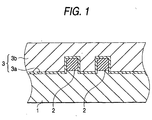
- FIG. 1 is a lateral cross-sectional view of an embodiment of a silica based optical waveguide according to the present invention.
- FIGS. 2A and 2B are graphs for explaining the dopant concentration distribution and the refractive index change by the dopant in the over cladding part in the case the refractive index increase in the P 2 O 5 segregation layer is offset by the fluorine addition.
- FIGS. 3A and 3B are graphs for explaining the dopant concentration distribution and the refractive index change by the dopant in the over cladding part in the case the refractive index increase in the P 2 O 5 segregation layer is offset by the B 2 O 3 amount increase.
- FIG. 4 is a graph showing the relationship between the P 2 O 5 concentration in the segregation layer and the number of generated crystals.
- FIG. 5 is a graph showing the relationship between the P 2 O 5 segregation layer thickness and the deviation of the transmitted central wavelength in the TE polarization and TM polarization (PD ⁇ ).
- FIG. 1 is a lateral cross-sectional view of an embodiment of a silica based optical waveguide according to the present invention.
- the numeral 1 denotes a substrate, 2 a core waveguide, 3 an over cladding part, 3a a segregation layer, and 3b a part of the over cladding part other than the segregation layer.
- the substrate 1 is a flat plate comprising a silica glass or silicon, or a such flat plate with an SiO 2 glass film formed on the surface thereof.
- the core waveguide 2 is provided by comprising the steps of forming a core glass film comprising a silica glass containing a dopant for increasing the refractive index, such as GeO 2 on the substrate 1 by a plasma Chemical Vapor Deposition (CVD) method, FHD method, or the like, and forming a circuit with a rectangular or square lateral cross-section, elongating in the longitudinal direction from the core glass film by a photolithography, a reactive ion etching, or the like.
- CVD Chemical Vapor Deposition
- the over cladding part 3 is a glass layer comprising a silica glass as the main composition, formed on the substrate 1 so as to cover the core waveguide 2, with a refractive index lower than that of the core waveguide 2 and substantially same as that of the substrate 1.
- the over cladding part 3 is a glass layer that is provided by comprising the steps of forming a porous silica based glass layer by accumulating glass fine particles comprising a silica glass containing a refractive index lowering dopant such as B 2 O 3 and a refractive index increasing dopant such as P 2 O 5 on the substrate 1 by FHD method so as to cover the core waveguide 2, and sintering the porous silica based glass layer for transmitting the light in the core.
- the porous silica based glass layer can also be formed by a CVD method, or a plasma CVD method.
- porous silica based glass layer formation by accumulating the glass fine particles with the substrate 1 provided with the core waveguide 2 heated at 500°C to 700°C, a porous silica based glass layer having a segregation layer with a concentration of the refractive index increasing dopant P 2 O 5 higher than the other part in the part in contact with the substrate and the core waveguide can be formed.
- the refractive index lowering dopant B 2 O 3 is provided with a uniform concentration without segregation.
- the P 2 O 5 concentration in the P 2 O 5 segregation layer and the thickness of the segregation layer can be adjusted according to the material gas supply amount and the substrate heating temperature. Furthermore, since the substrate can be heated homogeneously by forming the entirety or the principal part of the turn table to be used for the porous silica based glass layer formation on the substrate 1 with silicon, supporting the substrate 1 by a holder comprising silicon, and placing the same on a part of the rotating turn table comprising silicon for heating by a heater disposed below the turn table because of good heat conduction of silicon, the concentration and the thickness of the P 2 O 5 segregation layer can be uniform.
- the substrate with the porous silica based glass layer formed is heated in a fluorine gas atmosphere containing an SiF 4 , and a helium gas. Thereby, fluorine is taken into the porous silica based glass layer. In this state, with the SiF 4 supply stopped, the heating operation is continued only with the helium gas for transparent vitrification of the porous silica based glass layer so as to provide the over cladding part 3.
- the fluorine concentration in the P 2 O 5 segregation layer part away from the over cladding part surface can be made higher and the fluorine concentration in the other part lower so as to segregate fluorine.
- the segregation layer 3a of about a 1.5 ⁇ m to about 5 ⁇ m thickness with a higher P 2 O 5 concentration is formed in the part of the over cladding part 3 in contact with the substrate 1 and the core waveguide 2.
- the fluorine concentration and the thickness of the fluorine-segregated part can be adjusted by the SiF 4 concentration in the fluorine gas atmosphere, and the heating temperature and heating time under or without the existence of the SiF 4 , the thickness thereof is matched with the P 2 O 5 segregation layer thickness.
- the P 2 O 5 concentration in the P 2 O 5 segregation layer is adjusted to be 1% by weight to 15% by weight with the fluorine concentration to a degree sufficient for offsetting the refractive index increase by the P 2 O 5 by the refractive index decline by B 2 O 3 and fluorine.
- FIGS. 2A, 2B are graphs for explaining the dopant concentration distribution and the refractive index change by the dopant in the over cladding part.
- the vertical axis represents the distance from the substrate or the core waveguide in the over cladding part
- the lateral axis represents the dopant concentration in FIG. 2A, and the refractive index change in FIG. 2B.
- the segregation layer is formed in the part of the over cladding part close to the substrate or the core waveguide, with a relatively high P 2 O 5 and fluorine concentration in the segregation layer with respect to the other part.
- the B 2 O 3 concentration is same as the other part.
- the refractive index is changed drastically to the + side in the segregation layer, and it is changed slightly to the + side in the other part by P 2 O 5 .
- the refractive index is changed drastically to the - side in the segregation layer, and it is changed slightly to the - side in the other part by fluorine.
- the refractive index is changed uniformly to the - side by B 2 O 3 .
- the concentration of each dopant is adjusted such that the total refractive index change brought about by P 2 O 5 , fluorine, and B 2 O 3 can be substantially zero in the segregation layer part and the other part.
- the B 2 O 3 amount is changed by supplying the material gas for producing B 2 O 3 initially by a large amount and halfway by a reduced amount so that the B 2 O 3 amount added in the P 2 O 5 segregation layer is increased with respect to the B 2 O 3 amount in the other part. Accordingly, the refractive index increase derived from a high P 2 O 5 concentration in the P 2 O 5 segregation layer can be offset by the refractive index decline by the refractive index decline derived from the increase of the B 2 O 3 amount.
- FIGS. 3A, 3B are graphs for explaining the dopant concentration distribution and the refractive index change by the dopant in the over cladding part in that case.
- the vertical axis represents the distance from the substrate or the core waveguide in the over cladding part, and the lateral axis represents the dopant concentration in FIG. 3A, and the refractive index change in FIG. 3B.
- the P 2 O 5 segregation layer is formed in the part of the over cladding part close to the substrate or the core waveguide, with a relatively high P 2 O 5 and B 2 O 3 concentration in the segregation layer with respect to the other part.
- the refractive index is changed drastically to the + side in the segregation layer, and it is changed slightly to the + side in the other part by P 2 O 5 .
- the refractive index is changed drastically to the - side in the segregation layer, and it is changed slightly to the - side in the other part by B 2 O 3 .
- the concentration of each dopant is adjusted such that the total refractive index change brought about by P 2 O 5 , and B 2 O 3 can be substantially zero in the segregation layer part and the other part.
- FIG. 4 is a graph showing the relationship between the P 2 O 5 concentration in the segregation layer and the number of generated crystals. According to the graph, the number of the generated crystal can be zero with a 1% by weight or more P 2 O 5 concentration in the P 2 O 5 segregation layer.
- the thickness of the P 2 O 5 segregation layer for restraining the crystal generation can be any size, however, 1.5 ⁇ m or more is preferable for the production convenience. Furthermore, FIG.
- FIG 5 is a graph showing the relationship between the P 2 O 5 segregation layer thickness and the deviation of the transmitted central wavelength in the TE polarization and TM polarization (PD ⁇ ). According to the graph, the smaller the segregation layer thickness is, the smaller the PD ⁇ becomes so that the polarization dependency is improved. Moreover, with a 5 ⁇ m or less segregation layer thickness, the PD ⁇ is 0.03 nm or less, and thus a trouble is not caused in the practical use.
- the part of the substrate 1 in contact with the core waveguide 2 be projected at least by the segregation layer 3a thickness with respect to the other part of the substrate 1. According to the configuration, since the part in the vicinity of the core waveguide, having a larger P 2 O 5 concentration can further be reduced, the polarization dependency by the anisotropic thermal distortion can further be restrained in the core waveguide based on the thermal expansion coefficient difference in the substrate and the over cladding part surrounding the core waveguide.
- Example 1 the following silica based optical waveguide was produced.
- a core glass film made of SiO 2 with GeO 2 doped was formed on a substrate made of a silica glass with a 0.5 mm thickness and a 10 cm diameter by a plasma CVD method.
- the core glass film thickness was 6 ⁇ m, and the specific relative index difference with respect to the silica glass substrate was 0.75%.
- AWG arrayed Waveguide Grating
- the substrate with the core waveguide formed was gripped by a holder made of silicon so as to be placed on a part of a turn table, made of silicon. While rotating and heating the turn table at 600°C by a heater disposed below the turn table, a porous silica based glass layer made of SiO 2 with P 2 O 5 and B 2 O 3 doped was formed on the substrate by FHD method.
- the substrate with the porous silica based glass layer formed was placed in a sintering furnace so as to be heated at 1,000°C for one hour under an atmosphere of an SiF 4 /helium gas mixture being introduced. Thereafter, the SiF 4 supply was stopped so that it was heated at 1,300°C for one hour under a helium gas atmosphere being introduced for transparent vitrification of the porous silica based glass layer.
- a silica based optical waveguide having AWG circuit with a 30 ⁇ m thickness over cladding part formed on the substrate, covering the core waveguide was obtained. Crystal growth at the interface between the over cladding part and the core waveguide in the silica based optical waveguide was examined. Crystal growth was not found. Moreover, a part of the silica based optical waveguide was cut to measure the concentration of each dopant in the over cladding part. As a result, a segregation layer with a higher P 2 O 5 concentration was produced in the part of the over cladding part in contact with the substrate and the core waveguide, with a 4 ⁇ m thickness, and a 1.8% by weight P 2 O 5 concentration.
- a fluorine segregation layer was produced in the same part, with a 4 ⁇ m thickness, and a 0.5% by weight fluorine concentration.
- the P 2 O 5 concentration was 1.2% by weight, and the fluorine concentration was 0.1% by weight or less.
- the B 2 O 3 concentration was 1.5% by weight in the entire over cladding part, and it was not segregated.
- the optical characteristics of the silica based optical waveguide having the AWG circuit were evaluated. Extremely good values, that is, the insertion loss of 3 dB to 4 dB, the cross talk of -28 dB to -35 dB, and the deviation of the transmitted central wavelength in the TE polarization and TM polarization (also referred to as the PD ⁇ ) of 0.015 nm for each channel were provided.
- Example 2 the following silica based optical waveguide was produced.
- a silicon flat plate having a 1.0 mm thickness and a 10 cm diameter with an SiO 2 glass film whose thickness is 15 ⁇ m formed by a plasma CVD method used as a substrate
- a core glass film made of SiO 2 with GeO 2 doped was formed on the substrate by a plasma CVD method.
- the core glass film thickness was 6 ⁇ m
- the specific relative index difference with respect to the silica glass substrate was 0.75%.
- a core waveguide comprising AWG circuit was produced from the core glass film by a photolithography and a reactive ion etching.
- the substrate with the core waveguide formed was gripped by a holder made of silicon so as to be placed on a part of a turn table, made of silicon. While rotating and heating the turn table at 500°C by a heater disposed below the turn table, a porous silica based glass layer made of SiO 2 with P 2 O 5 and B 2 O 3 doped was formed on the substrate by FHD method.
- the B material introduced amount for the initial four times of the burner traverses was set to be eight times as much as the subsequent forty times of the burner traverses.
- the substrate with the porous silica based glass layer formed was placed in a sintering furnace so as to be heated at 1,100°C for two hours under a helium gas atmosphere for transparent vitrification of the porous silica based glass layer so as to provide the over cladding part.
- a silica based optical waveguide having AWG circuit with a 30 ⁇ m thickness over cladding part formed on the substrate, covering the core waveguide was obtained. Crystal growth at the interface between the over cladding part and the core waveguide in the silica based optical waveguide was examined. Crystal growth was not found. Moreover, a part of the silica based optical waveguide was cut to measure the concentration of each dopant in the over cladding part. As a result, a segregation layer with a higher P 2 O 5 concentration was produced in the part of the over cladding part in contact with the substrate and the core waveguide, with about a 5 ⁇ m thickness, and a 10% by weight P 2 O 5 concentration.
- a B 2 O 3 concentration was also high at the side close to the core waveguide and the substrate.
- the B 2 O 3 concentration in the part was 15% by weight, and the thickness of the part was about 5 ⁇ m.
- the P 2 O 5 concentration was 8% by weight, and the B 2 O 3 concentration was 12% by weight.
- the optical characteristics of the silica based optical waveguide having the AWG circuit were evaluated. Practically good values, that is, the insertion loss of 3 dB to 4 dB, the cross talk of -25 dB to -32 dB, and the deviation of the transmitted central wavelength in the TE polarization and TM polarization (also referred to as the PD ⁇ ) of 0.03 nm were provided for each channel.
- the following silica based optical waveguide was produced.
- the process to the formation of the porous silica based glass layer on the substrate was same as the Example 1.
- the substrate with the porous silica based glass layer formed was placed in a sintering furnace so as to be heated at 1,300°C for one hour under a helium gas atmosphere for transparent vitrification of the porous silica based glass layer.
- a silica based optical waveguide having AWG circuit with a 30 ⁇ m thickness over cladding part formed on the substrate, covering the core waveguide was obtained. Crystal growth at the interface between the over cladding part and the core waveguide in the silica based optical waveguide was examined. Crystal growth was not found.
- a part of the silica based optical waveguide was cut to measure the concentration of each dopant in the over cladding part.
- a segregation layer with a higher P 2 O 5 concentration was produced in the part of the over cladding part in contact with the substrate and the core waveguide, with a 4 ⁇ m thickness, and a 1.8% by weight P 2 O 5 concentration.
- the P 2 O 5 concentration was 1.2% by weight.
- the B 2 O 3 concentration was 1.5% by weight in the entire over cladding part, and it was not segregated.
- the optical characteristics of the silica based optical waveguide having the AWG circuit were evaluated.
- the insertion loss was 3 dB to 4 dB
- the cross talk was -20 dB to -27 dB
- the deviation of the transmitted central wavelength in the TE polarization and TM polarization was 0.04 nm, and thus the cross talk and the deviation of the transmitted central wavelength were large compared with the Examples 1 and 2 for each channel.
- the following silica based optical waveguide was produced.
- the process to the formation of the core waveguide on the substrate was same as the Example 1.
- the porous silica based glass layer was formed on the substrate in the same process as the Example 1 except that the turn table heating temperature was changed to 300°C.
- the substrate with the porous silica based glass layer formed was placed in a sintering furnace so as to be heated at 1,300°C for one hour under a helium gas atmosphere for transparent vitrification of the porous silica based glass layer.
- a silica based optical waveguide having AWG circuit with a 30 ⁇ m thickness over cladding part formed on the substrate, covering the core waveguide was obtained.
- the interface between the over cladding part and the core waveguide in the silica based optical waveguide was examined. Crystals were found like dots. Moreover, a part of the silica based optical waveguide was cut to measure the concentration of each dopant in the over cladding part. As a result, the P 2 O 5 concentration was 1.3% by weight in the entire over cladding part without segregation. The B 2 O 3 concentration was 1.5% by weight in the entire over cladding part without segregation. Furthermore, the optical characteristics of the silica based optical waveguide having the AWG circuit were evaluated.
- the insertion loss was 5 dB to 8 dB, and the cross talk was -15 dB to -20 dB, and thus the optical characteristics were much poorer than the Examples 1 and 2 for each channel. Moreover, it is poorer than the Comparative Example 1.
- a silica based optical waveguide according to the present invention comprises a substrate, a core waveguide formed on the substrate, and an over cladding part formed on the substrate so as to cover the core waveguide, wherein a segregation layer with a higher concentration of a refractive index increasing dopant is formed in a part of the over cladding part in contact with the substrate and the core waveguide such that at least a part of the refractive index increase in the segregation layer with respect to the part of the over cladding part other than the segregation layer is offset by decline of the refractive index by increasing the amount of a refractive index lowering dopant added in the segregation layer and/or adding another refractive index lowering dopant, the refractive index of the segregation layer in the over cladding part can be lowered to a level substantially same as that of the other part. Therefore, since a high refractive index by the segregation layer can be alleviated, interference among circuits can hardly be generated even in the case
- the polarization dependency by the anisotropic thermal distortion can be restrained in the core waveguide based on the thermal expansion coefficient difference in the substrate and the over cladding part surrounding the core waveguide. Furthermore, the crystal growth at the interface between the over cladding part and the core waveguide can be restrained so as to provide an optical waveguide with a small propagation loss. Moreover, by offsetting the refractive index increase in the P 2 O 5 segregation layer by addition of fluorine, since the fluorine addition causes decline of the thermal expansion coefficient so that the difference in the thermal expansion coefficient between the over cladding part and the substrate can be reduced, the polarization dependency derived from generation of the thermal distortion can further be reduced.
Landscapes
- Physics & Mathematics (AREA)
- General Physics & Mathematics (AREA)
- Optics & Photonics (AREA)
- Engineering & Computer Science (AREA)
- Microelectronics & Electronic Packaging (AREA)
- Optical Integrated Circuits (AREA)
Applications Claiming Priority (4)
| Application Number | Priority Date | Filing Date | Title |
|---|---|---|---|
| JP2000003515 | 2000-01-12 | ||
| JP2000003515 | 2000-01-12 | ||
| JP2000156269 | 2000-05-26 | ||
| JP2000156269A JP3551895B2 (ja) | 2000-01-12 | 2000-05-26 | 石英系光導波路及びその製造方法 |
Publications (3)
| Publication Number | Publication Date |
|---|---|
| EP1116966A2 true EP1116966A2 (de) | 2001-07-18 |
| EP1116966A3 EP1116966A3 (de) | 2004-02-11 |
| EP1116966A9 EP1116966A9 (de) | 2004-05-26 |
Family
ID=26583374
Family Applications (1)
| Application Number | Title | Priority Date | Filing Date |
|---|---|---|---|
| EP00128413A Withdrawn EP1116966A3 (de) | 2000-01-12 | 2000-12-27 | Polarisationsunabhängiger optischer Wellenleiter aus Silica |
Country Status (8)
| Country | Link |
|---|---|
| US (1) | US6690872B2 (de) |
| EP (1) | EP1116966A3 (de) |
| JP (1) | JP3551895B2 (de) |
| KR (1) | KR20010070514A (de) |
| CN (1) | CN1214261C (de) |
| AU (1) | AU1367701A (de) |
| CA (1) | CA2332385A1 (de) |
| TW (1) | TW508462B (de) |
Families Citing this family (16)
| Publication number | Priority date | Publication date | Assignee | Title |
|---|---|---|---|---|
| US6836608B2 (en) * | 2000-12-28 | 2004-12-28 | Matsushita Electric Industrial Co., Ltd. | Planar optical waveguide, method for manufacturing the same and polymer optical waveguide |
| JP2003014959A (ja) * | 2001-07-03 | 2003-01-15 | Furukawa Electric Co Ltd:The | 光導波路 |
| US6947653B2 (en) * | 2001-10-12 | 2005-09-20 | Jds Uniphase Corporation | Waveguide stress engineering and compatible passivation in planar lightwave circuits |
| JP2003149479A (ja) * | 2001-11-14 | 2003-05-21 | Hitachi Cable Ltd | 石英系ガラス光導波路及びそれを用いた光モジュール |
| US6950591B2 (en) * | 2002-05-16 | 2005-09-27 | Corning Incorporated | Laser-written cladding for waveguide formations in glass |
| JP4224259B2 (ja) * | 2002-05-28 | 2009-02-12 | パナソニック電工株式会社 | 光電気混載基板の製造方法 |
| JP4439191B2 (ja) | 2002-06-07 | 2010-03-24 | 三洋電機株式会社 | 光導波路およびこれを用いた光送受信モジュール |
| US20040037531A1 (en) * | 2002-08-20 | 2004-02-26 | Andrews Mark P. | Waveguide device with a tailored thermal response |
| JP3936665B2 (ja) * | 2003-02-17 | 2007-06-27 | Tdk株式会社 | 光導波路 |
| JP2006119379A (ja) * | 2004-10-21 | 2006-05-11 | Sumitomo Electric Ind Ltd | 光導波路デバイスの製造方法、および光導波路デバイス |
| CN104678493A (zh) * | 2013-12-01 | 2015-06-03 | 无锡宏纳科技有限公司 | 一种平面光波导分路器波导分叉的填充方法 |
| KR20190028514A (ko) * | 2016-07-15 | 2019-03-18 | 코닝 인코포레이티드 | 적층 구조의 광 도파관 물품 및 이를 형성하는 방법 |
| CN108646345B (zh) * | 2018-05-16 | 2020-04-14 | 德州尧鼎光电科技有限公司 | 一种深紫外平面光波导制作方法 |
| CN108427159B (zh) * | 2018-05-16 | 2020-04-14 | 德州尧鼎光电科技有限公司 | 一种深紫外平面光波导 |
| CN115912026B (zh) * | 2022-11-29 | 2025-06-27 | 吉林大学 | 一种基于铒镱共掺聚合物复合结构芯层的光波导放大器及其制备方法 |
| CN116165741A (zh) * | 2023-03-06 | 2023-05-26 | 珠海庞纳微半导体科技有限公司 | 光波导及其制备方法、光器件和光电集成芯片 |
Family Cites Families (7)
| Publication number | Priority date | Publication date | Assignee | Title |
|---|---|---|---|---|
| US4896942A (en) * | 1989-02-03 | 1990-01-30 | Minnesota Mining And Manufacturing Company | Polarization-maintaining optical fiber |
| GB9202463D0 (en) * | 1992-02-05 | 1992-03-18 | British Telecomm | Silica waveguide structure |
| JPH0627342A (ja) * | 1992-07-13 | 1994-02-04 | Hitachi Cable Ltd | ガラス導波路 |
| TW243500B (de) * | 1993-01-14 | 1995-03-21 | Sumitomo Electric Industries | |
| JPH07318734A (ja) | 1994-05-27 | 1995-12-08 | Hitachi Cable Ltd | 石英系ガラス導波路及びその製造方法 |
| JP3203178B2 (ja) * | 1996-02-27 | 2001-08-27 | 日立電線株式会社 | 光導波路、光モジュール及び光システム |
| CA2247970A1 (en) * | 1997-10-29 | 1999-04-29 | Corning Incorporated | Method of making segmented core optical waveguide preforms |
-
2000
- 2000-05-26 JP JP2000156269A patent/JP3551895B2/ja not_active Expired - Fee Related
- 2000-12-27 EP EP00128413A patent/EP1116966A3/de not_active Withdrawn
-
2001
- 2001-01-09 TW TW090100435A patent/TW508462B/zh active
- 2001-01-09 CA CA002332385A patent/CA2332385A1/en not_active Abandoned
- 2001-01-10 US US09/756,869 patent/US6690872B2/en not_active Expired - Fee Related
- 2001-01-11 KR KR1020010001614A patent/KR20010070514A/ko not_active Withdrawn
- 2001-01-11 AU AU13677/01A patent/AU1367701A/en not_active Abandoned
- 2001-01-12 CN CNB01101265XA patent/CN1214261C/zh not_active Expired - Fee Related
Also Published As
| Publication number | Publication date |
|---|---|
| CN1304052A (zh) | 2001-07-18 |
| US6690872B2 (en) | 2004-02-10 |
| CN1214261C (zh) | 2005-08-10 |
| US20010007606A1 (en) | 2001-07-12 |
| AU1367701A (en) | 2001-07-19 |
| JP3551895B2 (ja) | 2004-08-11 |
| TW508462B (en) | 2002-11-01 |
| KR20010070514A (ko) | 2001-07-25 |
| CA2332385A1 (en) | 2001-07-12 |
| JP2001264563A (ja) | 2001-09-26 |
| EP1116966A3 (de) | 2004-02-11 |
| EP1116966A9 (de) | 2004-05-26 |
Similar Documents
| Publication | Publication Date | Title |
|---|---|---|
| US6690872B2 (en) | Silica based optical waveguide and production method therefor | |
| US7372121B2 (en) | GeBPSG top clad for a planar lightwave circuit | |
| GB2181862A (en) | Method of making a planar lightwave guide | |
| EP0803589B1 (de) | Verfahren zur Herstellung eines blasenfreien Lichtwellenleiters | |
| US6795631B2 (en) | Optical waveguide apparatus and method of producing the same | |
| KR100322126B1 (ko) | 광도파로 제작용 기판 및 그 제작방법 | |
| EP1560046A1 (de) | Lichtwellenleiter und Herstellungsverfahren dafür | |
| JPH05100123A (ja) | 光導波路の製造方法 | |
| EP1209493A1 (de) | Optischer Wellenleiter und Methode zur Herstellung desselben | |
| JP2682919B2 (ja) | 光導波路及びその製造方法 | |
| US20220179151A1 (en) | Optical waveguide and manufacturing method thereof | |
| JP2000147293A (ja) | 基板型光導波路およびその製造方法 | |
| JP2953173B2 (ja) | 光導波路 | |
| EP1074864A2 (de) | Verfahren zur Herstellung planarer optischer Wellenleitervorrichtungen | |
| JP2001074959A (ja) | 埋め込み型光導波路及びその製造方法 | |
| KR100219751B1 (ko) | 다량의 붕소첨가로 실리카 평판도파박막 및 평판도파로의 복굴절을 줄이는 방법 | |
| JP2927597B2 (ja) | ガラス導波路の製造法 | |
| JP2000241636A (ja) | 石英系ガラス導波路及びその製造方法 | |
| JP3840835B2 (ja) | 石英系ガラス導波路素子の製造方法 | |
| JPH11271542A (ja) | ガラス導波路及びその製造方法 | |
| JPH07318739A (ja) | 石英系光導波路とその製造方法 | |
| JPH08106022A (ja) | 光導波路の製造方法 | |
| JPH0627342A (ja) | ガラス導波路 | |
| JP2002040275A (ja) | 光導波路の製造方法 | |
| JPH07306325A (ja) | 石英系光導波路とその製造方法 |
Legal Events
| Date | Code | Title | Description |
|---|---|---|---|
| PUAI | Public reference made under article 153(3) epc to a published international application that has entered the european phase |
Free format text: ORIGINAL CODE: 0009012 |
|
| AK | Designated contracting states |
Kind code of ref document: A2 Designated state(s): AT BE CH CY DE DK ES FI FR GB GR IE IT LI LU MC NL PT SE TR |
|
| AX | Request for extension of the european patent |
Free format text: AL;LT;LV;MK;RO;SI |
|
| PUAL | Search report despatched |
Free format text: ORIGINAL CODE: 0009013 |
|
| AK | Designated contracting states |
Kind code of ref document: A3 Designated state(s): AT BE CH CY DE DK ES FI FR GB GR IE IT LI LU MC NL PT SE TR |
|
| AX | Request for extension of the european patent |
Extension state: AL LT LV MK RO SI |
|
| RIN1 | Information on inventor provided before grant (corrected) |
Inventor name: HIROSE, CHISAI,SUMIOMO ELECTRIC IND. LTD. Inventor name: TANAKA, SHIGERU,SUMIOMO ELECTRIC IND. LTD. Inventor name: AKASAKA, NOBUHIRO,SUMIOMO ELECTRIC IND. LTD. Inventor name: HIRAI, SHIGERU,SUMIOMO ELECTRIC IND. LTD. Inventor name: SASAKI, TAKASHI,SUMITOMO ELECTRIC IND. LTD. |
|
| RIN1 | Information on inventor provided before grant (corrected) |
Inventor name: HIROSE, CHISAI,SUMITOMO ELECTRIC IND. LTD. Inventor name: TANAKA, SHIGERU,SUMITOMO ELECTRIC IND. LTD. Inventor name: AKASAKA, NOBUHIRO,SUMITOMO ELECTRIC IND. LTD. Inventor name: HIRAI, SHIGERU,SUMITOMO ELECTRIC IND. LTD. Inventor name: SASAKI, TAKASHI,SUMITOMO ELECTRIC IND. LTD. |
|
| STAA | Information on the status of an ep patent application or granted ep patent |
Free format text: STATUS: THE APPLICATION HAS BEEN WITHDRAWN |
|
| 18W | Application withdrawn |
Effective date: 20040705 |