EP1119225A2 - Plaquette à circuits, boítier de connexion électrique comprenant cette plaquette, et procédé de fabrication de cette plaquette - Google Patents
Plaquette à circuits, boítier de connexion électrique comprenant cette plaquette, et procédé de fabrication de cette plaquette Download PDFInfo
- Publication number
- EP1119225A2 EP1119225A2 EP01300312A EP01300312A EP1119225A2 EP 1119225 A2 EP1119225 A2 EP 1119225A2 EP 01300312 A EP01300312 A EP 01300312A EP 01300312 A EP01300312 A EP 01300312A EP 1119225 A2 EP1119225 A2 EP 1119225A2
- Authority
- EP
- European Patent Office
- Prior art keywords
- bus bars
- circuit board
- holes
- insulation board
- board
- Prior art date
- Legal status (The legal status is an assumption and is not a legal conclusion. Google has not performed a legal analysis and makes no representation as to the accuracy of the status listed.)
- Granted
Links
- 238000004519 manufacturing process Methods 0.000 title claims description 7
- 238000009413 insulation Methods 0.000 claims abstract description 39
- 238000003466 welding Methods 0.000 claims description 21
- 238000005304 joining Methods 0.000 claims description 8
- 238000000034 method Methods 0.000 claims description 8
- 239000000969 carrier Substances 0.000 description 14
- 239000011295 pitch Substances 0.000 description 11
- 239000002184 metal Substances 0.000 description 7
- 230000015572 biosynthetic process Effects 0.000 description 6
- 230000035515 penetration Effects 0.000 description 6
- 239000000463 material Substances 0.000 description 4
- 238000003475 lamination Methods 0.000 description 3
- 238000005520 cutting process Methods 0.000 description 2
- 238000000465 moulding Methods 0.000 description 2
- 238000003491 array Methods 0.000 description 1
- 238000010276 construction Methods 0.000 description 1
- 238000005336 cracking Methods 0.000 description 1
- 230000020169 heat generation Effects 0.000 description 1
- 238000009434 installation Methods 0.000 description 1
- 239000012774 insulation material Substances 0.000 description 1
- 239000010410 layer Substances 0.000 description 1
- 238000012986 modification Methods 0.000 description 1
- 230000004048 modification Effects 0.000 description 1
- 239000002991 molded plastic Substances 0.000 description 1
- 238000002360 preparation method Methods 0.000 description 1
- 238000003825 pressing Methods 0.000 description 1
- 239000002356 single layer Substances 0.000 description 1
Images



Classifications
-
- H—ELECTRICITY
- H05—ELECTRIC TECHNIQUES NOT OTHERWISE PROVIDED FOR
- H05K—PRINTED CIRCUITS; CASINGS OR CONSTRUCTIONAL DETAILS OF ELECTRIC APPARATUS; MANUFACTURE OF ASSEMBLAGES OF ELECTRICAL COMPONENTS
- H05K3/00—Apparatus or processes for manufacturing printed circuits
- H05K3/40—Forming printed elements for providing electric connections to or between printed circuits
- H05K3/4038—Through-connections; Vertical interconnect access [VIA] connections
- H05K3/4084—Through-connections; Vertical interconnect access [VIA] connections by deforming at least one of the conductive layers
-
- H—ELECTRICITY
- H01—ELECTRIC ELEMENTS
- H01R—ELECTRICALLY-CONDUCTIVE CONNECTIONS; STRUCTURAL ASSOCIATIONS OF A PLURALITY OF MUTUALLY-INSULATED ELECTRICAL CONNECTING ELEMENTS; COUPLING DEVICES; CURRENT COLLECTORS
- H01R12/00—Structural associations of a plurality of mutually-insulated electrical connecting elements, specially adapted for printed circuits, e.g. printed circuit boards [PCB], flat or ribbon cables, or like generally planar structures, e.g. terminal strips, terminal blocks; Coupling devices specially adapted for printed circuits, flat or ribbon cables, or like generally planar structures; Terminals specially adapted for contact with, or insertion into, printed circuits, flat or ribbon cables, or like generally planar structures
- H01R12/50—Fixed connections
- H01R12/51—Fixed connections for rigid printed circuits or like structures
- H01R12/52—Fixed connections for rigid printed circuits or like structures connecting to other rigid printed circuits or like structures
- H01R12/526—Fixed connections for rigid printed circuits or like structures connecting to other rigid printed circuits or like structures the printed circuits being on the same board
-
- H—ELECTRICITY
- H05—ELECTRIC TECHNIQUES NOT OTHERWISE PROVIDED FOR
- H05K—PRINTED CIRCUITS; CASINGS OR CONSTRUCTIONAL DETAILS OF ELECTRIC APPARATUS; MANUFACTURE OF ASSEMBLAGES OF ELECTRICAL COMPONENTS
- H05K1/00—Printed circuits
- H05K1/02—Details
- H05K1/0286—Programmable, customizable or modifiable circuits
- H05K1/0287—Programmable, customizable or modifiable circuits having an universal lay-out, e.g. pad or land grid patterns or mesh patterns
- H05K1/0289—Programmable, customizable or modifiable circuits having an universal lay-out, e.g. pad or land grid patterns or mesh patterns having a matrix lay-out, i.e. having selectively interconnectable sets of X-conductors and Y-conductors in different planes
-
- H—ELECTRICITY
- H01—ELECTRIC ELEMENTS
- H01R—ELECTRICALLY-CONDUCTIVE CONNECTIONS; STRUCTURAL ASSOCIATIONS OF A PLURALITY OF MUTUALLY-INSULATED ELECTRICAL CONNECTING ELEMENTS; COUPLING DEVICES; CURRENT COLLECTORS
- H01R29/00—Coupling parts for selective co-operation with a counterpart in different ways to establish different circuits, e.g. for voltage selection, for series-parallel selection, programmable connectors
-
- H—ELECTRICITY
- H01—ELECTRIC ELEMENTS
- H01R—ELECTRICALLY-CONDUCTIVE CONNECTIONS; STRUCTURAL ASSOCIATIONS OF A PLURALITY OF MUTUALLY-INSULATED ELECTRICAL CONNECTING ELEMENTS; COUPLING DEVICES; CURRENT COLLECTORS
- H01R43/00—Apparatus or processes specially adapted for manufacturing, assembling, maintaining, or repairing of line connectors or current collectors or for joining electric conductors
- H01R43/02—Apparatus or processes specially adapted for manufacturing, assembling, maintaining, or repairing of line connectors or current collectors or for joining electric conductors for soldered or welded connections
- H01R43/0214—Resistance welding
-
- H—ELECTRICITY
- H05—ELECTRIC TECHNIQUES NOT OTHERWISE PROVIDED FOR
- H05K—PRINTED CIRCUITS; CASINGS OR CONSTRUCTIONAL DETAILS OF ELECTRIC APPARATUS; MANUFACTURE OF ASSEMBLAGES OF ELECTRICAL COMPONENTS
- H05K2201/00—Indexing scheme relating to printed circuits covered by H05K1/00
- H05K2201/10—Details of components or other objects attached to or integrated in a printed circuit board
- H05K2201/10227—Other objects, e.g. metallic pieces
- H05K2201/10272—Busbars, i.e. thick metal bars mounted on the printed circuit board [PCB] as high-current conductors
-
- H—ELECTRICITY
- H05—ELECTRIC TECHNIQUES NOT OTHERWISE PROVIDED FOR
- H05K—PRINTED CIRCUITS; CASINGS OR CONSTRUCTIONAL DETAILS OF ELECTRIC APPARATUS; MANUFACTURE OF ASSEMBLAGES OF ELECTRICAL COMPONENTS
- H05K2203/00—Indexing scheme relating to apparatus or processes for manufacturing printed circuits covered by H05K3/00
- H05K2203/06—Lamination
- H05K2203/063—Lamination of preperforated insulating layer
-
- H—ELECTRICITY
- H05—ELECTRIC TECHNIQUES NOT OTHERWISE PROVIDED FOR
- H05K—PRINTED CIRCUITS; CASINGS OR CONSTRUCTIONAL DETAILS OF ELECTRIC APPARATUS; MANUFACTURE OF ASSEMBLAGES OF ELECTRICAL COMPONENTS
- H05K2203/00—Indexing scheme relating to apparatus or processes for manufacturing printed circuits covered by H05K3/00
- H05K2203/15—Position of the PCB during processing
- H05K2203/1572—Processing both sides of a PCB by the same process; Providing a similar arrangement of components on both sides; Making interlayer connections from two sides
-
- H—ELECTRICITY
- H05—ELECTRIC TECHNIQUES NOT OTHERWISE PROVIDED FOR
- H05K—PRINTED CIRCUITS; CASINGS OR CONSTRUCTIONAL DETAILS OF ELECTRIC APPARATUS; MANUFACTURE OF ASSEMBLAGES OF ELECTRICAL COMPONENTS
- H05K3/00—Apparatus or processes for manufacturing printed circuits
- H05K3/10—Apparatus or processes for manufacturing printed circuits in which conductive material is applied to the insulating support in such a manner as to form the desired conductive pattern
- H05K3/20—Apparatus or processes for manufacturing printed circuits in which conductive material is applied to the insulating support in such a manner as to form the desired conductive pattern by affixing prefabricated conductor pattern
- H05K3/202—Apparatus or processes for manufacturing printed circuits in which conductive material is applied to the insulating support in such a manner as to form the desired conductive pattern by affixing prefabricated conductor pattern using self-supporting metal foil pattern
Definitions
- This invention relates to a circuit board and to an electrical connection box containing such a circuit board, e.g. an electrical connection box for use in an automobile or other vehicle.
- the invention also relates to a method of making such a circuit board.
- a pressure welding system of wiring a wire such as a single core wire or the like along a circuit on an insulation board and connecting a pressure welding terminal on said wire by pressure welding It is also known to use bus bars formed by stamping an electro-conductive metal plate into a circuit board shape.
- bus bars when bus bars are used as an interior circuit, a mould for stamping must be made in accordance with the circuit, so that there are problems that the alternation of a circuit cannot be easily carried out and the costs of preparation of a mould costs high. Further, there are a lot of residual parts which are not used after stamping, so that the yield of the electro-conductive metal plate is poor, also raising cost. For example, if 7 or 8 sheets of bus bars must be arranged in multi-layer lamination with insulation boards between them because of a sharp increase of number of circuits accommodated in the inside of an electrical connection box, the cost is high.
- Insulation sheets 1a, 1b are laminated on both sides of an electro-conductive member 3 which is made in a lattice shape by stamping out the removed parts 3a of an electro-conductive metal plate.
- the circuit is formed by cutting the unwanted connection points 3b. Wiring is connected to the electro-conductive member 3 to make connection with exterior circuits. Since the circuit is formed by cutting the points 3b, variation of the circuit is easily achieved.
- the lattice-shape is formed by stamping and there are a lot of the removed parts 3a, there remains a problem that the yield of the electro-conductive metal plate is not improved.
- the present invention has as a first object to reduce the cost related to forming the interior circuit. Another object is to permit easy variation of a circuit.
- the subject is thirdly to design a cost reduction by being able to easily form insulation materials which lie between the third bus bars.
- the present invention provides a circuit board having an insulation board having first and second opposite main faces.
- a plurality of first strip bus bars are arranged on the first main face and extend in parallel in a first direction
- a plurality of second strip bus bars are arranged on the second main face and extend in parallel in a second direction crossing the first direction, whereby as seen in plan view on one of the main faces there is an array of crossing points of the bus bars.
- the insulation board has a plurality of holes through it at a plurality of the crossing points, at which both the mutually crossing bus bars are bent each towards each other and mutually joined through the board to establish electrical connection between them, whereby a predetermined wiring pattern is obtained.
- the bus bars are joined by welding, but other joining methods are possible. Resistance welding is most preferred.
- first bus bars are located in grooves in the first main face of the insulation board and the second bus bars are located in grooves in the second main face.
- the thickness of each of the mutually crossing bus bars in the direction of insulation board thickness is reduced, compared with the thickness of adjacent portions, by 15 to 25%.
- this thickness reduction is accompanied by elongating the bus bar by stretching, in order to provide the bent portion. This can avoid disturbance of the ends of the bus bars.
- the invention provides a method of making a circuit board, comprising the steps of:-
- one of the bent portion may have a protrusion directed towards the other of said mutually crossing pair of bus bars.
- the use of material of the bus bars can be efficient, so that the yield of the material can be improved. Further, stamping by a mold which has been specifically designed for the individual circuit required is unnecessary. Therefore the cost for formation of the circuit board can be greatly reduced.
- the bus bars respectively arranged in parallel in the two directions, which are typically orthogonal, may have a nominal thickness, in the thickness direction of the insulation board, in the range of 0.5mm to 1.0mm. Both ends thereof may be linked with carriers, and the carriers are cut to be removed after the bent parts are joined, e.g. resistance-welded.
- bus bars of the two directions are assembled on the insulation board, portions of them which are unnecessary in the circuit may be cut, after joining of the upper and lower bent parts, to form the requisite circuit. It is possible to use standard sets of the bus bars for both the two directions, to simplify and reduce cost.
- the pitches (spacing) of the strip bus bars can be selected to correspond with the spacings of terminals of exterior components, such as a connector, a fuse and a relay.
- some of the bus bars arranged in parallel in one direction may correspond with the terminal pitch of a fuse, while others correspond with the terminal pitch of a relay.
- Some of the bus bars arranged in the other direction may correspond with the small pitch of a connector terminal hole, others correspond with a middle-size pitch, and the remainder correspond with a large pitch.
- tabs connected with these bus bars can be directly connected with the connector, the fuse and the relay, etc.
- the present invention provides an electric connection box including the above circuit board.
- the circuit board of the above-described construction may be arranged as a single layer in the electric connection box, or a plural number of the circuit boards may be further arranged by lamination through insulation boards.
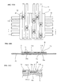
- Strip bus bars 14 are provided as parallel discrete spaced metal strips extending in an X direction on the upper face of an insulation board 11.
- Strip bus bars 15 are similarly provided as parallel discrete spaced metal strips extending in a Y direction, orthogonal to the X direction, on the lower face of the insulation board 11 at regular spacings.
- the strip bus bars 14, 15 of the X and Y directions are thus arranged crosswise through the insulation board 11 so as to form a lattice with mutual crossing points of the bus bars.
- the bus bars 14, 15 are located in recesses or grooves 11a, 11b in the upper and lower faces of the insulation board 11.
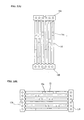
- the ends of the bus bars 14 of the X direction are initially linked with the carriers 16A, 16B, and may be arranged on the upper face of the insulation board 11 in this condition, but as indicated by Fig. 1(A) in this embodiment the carrier 16B is cut off after the formation of the bent parts 14a described below and before the bus bars 14 are placed on the board 11.
- the width of the bus bars 14 is 2mm, and their nominal thickness is 0.64mm.
- the spacings (pitches) of the parallel bus bars 14 of the X direction may, as desired, be varied. For example, some may have a pitch of 4mm, others a pitch of 10mm and yet others a pitch of 6.8mm, corresponding with the spacing of terminals of a connector, a fuse and a relay.
- the bus bars 15 of the Y direction are similar. Both ends in their longitudinal direction when formed are linked with the carriers 17A, 17B, and the bus bars 15 are arranged on the lower face of the insulation board 10 in this condition.
- the bus bars 15 have a width of 2mm, a nominal thickness of 0.64mm and a uniform pitch of 4mm.
- the board thickness of the parts 11c between the respective bottom faces of the grooves 11a and 11b are as thin as 0.8mm at the cross positions. At the crossing points where the upper and lower bus bars are to be connected penetration holes 11d are provided.
- the penetration holes 11d provide a clearance since their upper parts 11d-1 are larger than the width of bus bars, and their lower parts 11d-2 are enlarged in a taper manner.
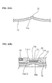
- the amount of protrusion of the bent parts 14a, 15a of the upper and lower bus bars 14, 15, which are resistance-welded through the penetration holes 11d, is thus fixed at half (0.4mm) of the board thickness of 0.8mm.
- the protruding faces are mutually brought in contact.
- the parts 14a, 15a are bent in an approximately arc shape so as to protrude by 0.4mm by press working.
- the bus bars 14, 15 are extended in length by this press working so as to be reduced in thickness by 15 to 25% (20% in the present embodiment) of their nominal thickness.
- the bent parts 14a, 15a are made so that the dimension between the two ends of each bus bar before formation and after formation of the bent part may be the same.
- the bent parts 14b are formed by press working when both ends of the bus bars 14 of the X direction are linked to the carriers 16A, 16B. Even if the number of the bent parts 14b are different in each bus bar 14, the deviation in the end positions of the respective bus bars 14 does not occur, and distortion and cracking do not occur in the carriers 16A, 16B. The same applies for the bus bars 15 of the Y direction and the carriers 17A, 17B.
- the bus bars 14 can be arranged on the upper face of the insulation board 11 when linked with the carriers 16A, 16B, and the bus bars 15 can be arranged on the lower face of the insulation board 11 when linked with the carriers 17A, 17B. Then the bent parts 14a of the bus bars 14 protrude downwards in the penetration holes 11d, and the bent parts 15a of the bus bars 15 protrude upwards, to bring the faces of the upper and lower bent parts 14a, 15a in contact.
- the resistance welding is carried out by pressing the electrodes 50, 51 of a resistance welder on the bent parts 14a, 15a from above and below so that resistance welds 30 (see Fig. 1) are formed between the bus bars 14, 15.
- the carriers 16A and 16B of the bus bars 14 and the carriers 17A, 17B of the bus bars 15 are separated collectively.
- fine protrusions 20 of 0.3mm height are provided on the upper faces of the bent parts 15a of the bus bars 15 in the press working. Further, when the fine protrusions 20 are provided, the bent part 15a including the fine protrusion 20 is also formed by length extension so that that the thickness of the bus bar is reduced by 15 to 25%, and the dimension between the two ends of each bus bar 15 is the same as that before the formation of the bent part.
- the welding zone can be concentrated at a small area in resistance welding, so that heat generation occurs easily, and the welding quality can be raised.
- the circuit board 10 formed as described above is for example accommodated in the lower casing part of an electrical connection box and assembled by placing an upper casing part thereon.
- the casing is typically of moulded plastics material and has lateral openings to receive components which have terminals to engage the ends of the bus bars 14, 15 e.g. connectors, fuses and relays.
- a plurality of the circuit boards 10 may be arranged in a stack in a box by lamination through a further insulation board or boards.
- the arrays of strip bus bars are arranged to give a lattice shape on the upper and lower faces of an insulation board, penetration holes are provided on the insulation board at intersection points where conduction is required, and bent parts provided on the upper and lower bus bars are mutually joined through the penetration holes.
- the bus bars 14, 15 are in the form of parallel spaced discrete metal strips. They are preferably joined without use of bonding material, e.g. by resistance-welding. Thereby, the connection of the upper and lower bus bars can be securely and easily obtained, and variation of the circuits is simple to achieve.
- the bent parts are formed by reducing the bus bar thickness by 15 to 25%, the dimension between the ends of the bus bars is the same before and after the formation of bent parts. Therefore, the parallel bus bars can be processed when they are joined with the carriers. Accordingly, their installation on the insulation board is easy and the resistance welding can be carried out in a condition in which the positioning of the bus bars was accurately carried out, so that the quality of the resistance welding can be high.
Landscapes
- Engineering & Computer Science (AREA)
- Microelectronics & Electronic Packaging (AREA)
- Manufacturing & Machinery (AREA)
- Connection Or Junction Boxes (AREA)
- Multi-Conductor Connections (AREA)
- Connections Effected By Soldering, Adhesion, Or Permanent Deformation (AREA)
- Coupling Device And Connection With Printed Circuit (AREA)
Applications Claiming Priority (2)
| Application Number | Priority Date | Filing Date | Title |
|---|---|---|---|
| JP2000010732 | 2000-01-19 | ||
| JP2000010732A JP3799468B2 (ja) | 2000-01-19 | 2000-01-19 | 回路板の製造方法、該方法により製造された回路板および該回路板を備えた電気接続箱 |
Publications (3)
| Publication Number | Publication Date |
|---|---|
| EP1119225A2 true EP1119225A2 (fr) | 2001-07-25 |
| EP1119225A3 EP1119225A3 (fr) | 2003-05-07 |
| EP1119225B1 EP1119225B1 (fr) | 2004-08-04 |
Family
ID=18538719
Family Applications (1)
| Application Number | Title | Priority Date | Filing Date |
|---|---|---|---|
| EP01300312A Expired - Lifetime EP1119225B1 (fr) | 2000-01-19 | 2001-01-15 | Plaquette à circuits, boítier de connexion électrique comprenant cette plaquette, et procédé de fabrication de cette plaquette |
Country Status (4)
| Country | Link |
|---|---|
| US (1) | US6443737B2 (fr) |
| EP (1) | EP1119225B1 (fr) |
| JP (1) | JP3799468B2 (fr) |
| DE (1) | DE60104573T2 (fr) |
Cited By (2)
| Publication number | Priority date | Publication date | Assignee | Title |
|---|---|---|---|---|
| EP1530411A1 (fr) * | 2003-11-05 | 2005-05-11 | Sumitomo Wiring Systems, Ltd. | Ensemble de circuits ainsi que son procédé de fabrication, unité de distribution et substrat de barres omnibus |
| EP1926185A1 (fr) * | 2006-10-30 | 2008-05-28 | Omron Corporation | Procédé de soudure de terminal conducteur et structure de terminal conducteur |
Families Citing this family (6)
| Publication number | Priority date | Publication date | Assignee | Title |
|---|---|---|---|---|
| JP3446672B2 (ja) * | 1999-07-30 | 2003-09-16 | 住友電装株式会社 | 電気接続箱 |
| JP4097388B2 (ja) * | 2000-07-21 | 2008-06-11 | 住友電装株式会社 | ジャンクションボックスの組立方法および該方法で組み立てられたジャンクションボックス |
| DE10117798A1 (de) * | 2001-04-10 | 2002-12-05 | Bosch Gmbh Robert | Stecker |
| JP2016025229A (ja) * | 2014-07-22 | 2016-02-08 | 株式会社オートネットワーク技術研究所 | 回路構成体 |
| JP6287815B2 (ja) * | 2014-12-24 | 2018-03-07 | 株式会社オートネットワーク技術研究所 | 回路構成体の製造方法 |
| JP6440778B2 (ja) * | 2017-07-04 | 2018-12-19 | 古河電気工業株式会社 | 電線構造体、電気接続構造、並びに、電線構造体の製造方法 |
Family Cites Families (8)
| Publication number | Priority date | Publication date | Assignee | Title |
|---|---|---|---|---|
| US2019625A (en) * | 1934-03-30 | 1935-11-05 | Rca Corp | Electrical apparatus |
| US3290557A (en) * | 1962-02-23 | 1966-12-06 | Sippican Corp | Wiring device with selectively severable conductor for forming predetermined circuit pattern |
| GB1108903A (en) * | 1965-07-31 | 1968-04-10 | Amp Inc | Electrical plugboard assembly |
| JPS5832795B2 (ja) | 1980-03-18 | 1983-07-15 | 品川自動車電線株式会社 | マトリツクス配線用連続基板 |
| US4801765A (en) * | 1986-01-06 | 1989-01-31 | American Telephone And Telegraph Company, At&T Bell Laboratories | Electronic component package using multi-level lead frames |
| US4859806A (en) * | 1988-05-17 | 1989-08-22 | Microelectronics And Computer Technology Corporation | Discretionary interconnect |
| EP0600052B1 (fr) * | 1992-06-15 | 1996-04-17 | Dyconex Patente Ag | Procede pour la production de points de contact ulterieurement conditionnables sur des supports de circuit, ainsi que supports de circuit pourvus de tels points de contact. |
| JP3361738B2 (ja) * | 1998-01-29 | 2003-01-07 | 矢崎総業株式会社 | 屋内配線用接続箱 |
-
2000
- 2000-01-19 JP JP2000010732A patent/JP3799468B2/ja not_active Expired - Fee Related
-
2001
- 2001-01-12 US US09/758,389 patent/US6443737B2/en not_active Expired - Fee Related
- 2001-01-15 EP EP01300312A patent/EP1119225B1/fr not_active Expired - Lifetime
- 2001-01-15 DE DE60104573T patent/DE60104573T2/de not_active Expired - Lifetime
Cited By (2)
| Publication number | Priority date | Publication date | Assignee | Title |
|---|---|---|---|---|
| EP1530411A1 (fr) * | 2003-11-05 | 2005-05-11 | Sumitomo Wiring Systems, Ltd. | Ensemble de circuits ainsi que son procédé de fabrication, unité de distribution et substrat de barres omnibus |
| EP1926185A1 (fr) * | 2006-10-30 | 2008-05-28 | Omron Corporation | Procédé de soudure de terminal conducteur et structure de terminal conducteur |
Also Published As
| Publication number | Publication date |
|---|---|
| EP1119225A3 (fr) | 2003-05-07 |
| DE60104573D1 (de) | 2004-09-09 |
| DE60104573T2 (de) | 2005-08-04 |
| EP1119225B1 (fr) | 2004-08-04 |
| US20010009201A1 (en) | 2001-07-26 |
| US6443737B2 (en) | 2002-09-03 |
| JP3799468B2 (ja) | 2006-07-19 |
| JP2001203012A (ja) | 2001-07-27 |
Similar Documents
| Publication | Publication Date | Title |
|---|---|---|
| US6270361B1 (en) | Connection structure for bus bars | |
| EP0994639B1 (fr) | Plaquette de circuit en treillis | |
| US6670548B2 (en) | Electrical junction box for a vehicle | |
| EP1017133A2 (fr) | Boítier de connecteur électrique | |
| US6514091B2 (en) | Electrical junction box for a vehicle | |
| JP3694200B2 (ja) | バスバーの接続構造 | |
| EP1119225B1 (fr) | Plaquette à circuits, boítier de connexion électrique comprenant cette plaquette, et procédé de fabrication de cette plaquette | |
| US3185761A (en) | Fabricated circuit structure | |
| US6524113B1 (en) | Automobile junction box with replaceable busbar circuit blocks | |
| JPH08287810A (ja) | 連鎖状ヒューズリンクおよびその形成方法 | |
| JP2000307202A (ja) | 回路板および該回路板を収容した電気接続箱 | |
| JP3427780B2 (ja) | 回路板を収容した電気接続箱 | |
| KR20230009592A (ko) | 부스바 및 그 제조 방법 | |
| JP4070913B2 (ja) | 電気的接合構造体並びにその成形方法 | |
| JPS5855774Y2 (ja) | 電気回路パネル | |
| EP0959528B1 (fr) | Appareil de production de connexions de sertissage | |
| JPH10334958A (ja) | レーザ溶接構造 | |
| JP3364881B2 (ja) | ブスバー配線板の製造方法 | |
| JPH10334955A (ja) | バスバーのレーザ溶接構造 | |
| JP3757792B2 (ja) | ジャンクションボックス | |
| JP2006325301A (ja) | 回路構成体 | |
| EP0895310A2 (fr) | Boíte de connexion électrique et procédé de fabrication des bornes | |
| JP2001314020A (ja) | 電気接続箱及びそれに用いるブスバーの形成方法 | |
| JPH0973852A (ja) | 板状ヒューズの製造方法 | |
| JPH0766897B2 (ja) | ノイズフィルター用フレームおよびその製造方法 |
Legal Events
| Date | Code | Title | Description |
|---|---|---|---|
| PUAI | Public reference made under article 153(3) epc to a published international application that has entered the european phase |
Free format text: ORIGINAL CODE: 0009012 |
|
| 17P | Request for examination filed |
Effective date: 20010205 |
|
| AK | Designated contracting states |
Kind code of ref document: A2 Designated state(s): AT BE CH CY DE DK ES FI FR GB GR IE IT LI LU MC NL PT SE TR |
|
| AX | Request for extension of the european patent |
Free format text: AL;LT;LV;MK;RO;SI |
|
| PUAL | Search report despatched |
Free format text: ORIGINAL CODE: 0009013 |
|
| AK | Designated contracting states |
Designated state(s): AT BE CH CY DE DK ES FI FR GB GR IE IT LI LU MC NL PT SE TR |
|
| AX | Request for extension of the european patent |
Extension state: AL LT LV MK RO SI |
|
| 17Q | First examination report despatched |
Effective date: 20030724 |
|
| AKX | Designation fees paid |
Designated state(s): DE FR GB IT |
|
| GRAP | Despatch of communication of intention to grant a patent |
Free format text: ORIGINAL CODE: EPIDOSNIGR1 |
|
| GRAS | Grant fee paid |
Free format text: ORIGINAL CODE: EPIDOSNIGR3 |
|
| GRAA | (expected) grant |
Free format text: ORIGINAL CODE: 0009210 |
|
| AK | Designated contracting states |
Kind code of ref document: B1 Designated state(s): DE FR GB IT |
|
| REG | Reference to a national code |
Ref country code: GB Ref legal event code: FG4D |
|
| REG | Reference to a national code |
Ref country code: IE Ref legal event code: FG4D |
|
| REF | Corresponds to: |
Ref document number: 60104573 Country of ref document: DE Date of ref document: 20040909 Kind code of ref document: P |
|
| ET | Fr: translation filed | ||
| PLBE | No opposition filed within time limit |
Free format text: ORIGINAL CODE: 0009261 |
|
| STAA | Information on the status of an ep patent application or granted ep patent |
Free format text: STATUS: NO OPPOSITION FILED WITHIN TIME LIMIT |
|
| 26N | No opposition filed |
Effective date: 20050506 |
|
| PGFP | Annual fee paid to national office [announced via postgrant information from national office to epo] |
Ref country code: IT Payment date: 20060131 Year of fee payment: 6 |
|
| PGFP | Annual fee paid to national office [announced via postgrant information from national office to epo] |
Ref country code: GB Payment date: 20080109 Year of fee payment: 8 |
|
| PGFP | Annual fee paid to national office [announced via postgrant information from national office to epo] |
Ref country code: FR Payment date: 20080108 Year of fee payment: 8 |
|
| GBPC | Gb: european patent ceased through non-payment of renewal fee |
Effective date: 20090115 |
|
| PG25 | Lapsed in a contracting state [announced via postgrant information from national office to epo] |
Ref country code: IT Free format text: LAPSE BECAUSE OF NON-PAYMENT OF DUE FEES Effective date: 20070115 |
|
| REG | Reference to a national code |
Ref country code: FR Ref legal event code: ST Effective date: 20091030 |
|
| PG25 | Lapsed in a contracting state [announced via postgrant information from national office to epo] |
Ref country code: GB Free format text: LAPSE BECAUSE OF NON-PAYMENT OF DUE FEES Effective date: 20090115 |
|
| PG25 | Lapsed in a contracting state [announced via postgrant information from national office to epo] |
Ref country code: FR Free format text: LAPSE BECAUSE OF NON-PAYMENT OF DUE FEES Effective date: 20090202 |
|
| PGFP | Annual fee paid to national office [announced via postgrant information from national office to epo] |
Ref country code: DE Payment date: 20130109 Year of fee payment: 13 |
|
| REG | Reference to a national code |
Ref country code: DE Ref legal event code: R119 Ref document number: 60104573 Country of ref document: DE |
|
| REG | Reference to a national code |
Ref country code: DE Ref legal event code: R119 Ref document number: 60104573 Country of ref document: DE Effective date: 20140801 |
|
| PG25 | Lapsed in a contracting state [announced via postgrant information from national office to epo] |
Ref country code: DE Free format text: LAPSE BECAUSE OF NON-PAYMENT OF DUE FEES Effective date: 20140801 |