EP1120829A1 - Keramische platte für halbleiterproduktionsanordnung - Google Patents
Keramische platte für halbleiterproduktionsanordnung Download PDFInfo
- Publication number
- EP1120829A1 EP1120829A1 EP99961446A EP99961446A EP1120829A1 EP 1120829 A1 EP1120829 A1 EP 1120829A1 EP 99961446 A EP99961446 A EP 99961446A EP 99961446 A EP99961446 A EP 99961446A EP 1120829 A1 EP1120829 A1 EP 1120829A1
- Authority
- EP
- European Patent Office
- Prior art keywords
- wafer
- ceramic
- ceramic substrate
- board
- conductor layer
- Prior art date
- Legal status (The legal status is an assumption and is not a legal conclusion. Google has not performed a legal analysis and makes no representation as to the accuracy of the status listed.)
- Withdrawn
Links
Images



Classifications
-
- H—ELECTRICITY
- H10—SEMICONDUCTOR DEVICES; ELECTRIC SOLID-STATE DEVICES NOT OTHERWISE PROVIDED FOR
- H10P—GENERIC PROCESSES OR APPARATUS FOR THE MANUFACTURE OR TREATMENT OF DEVICES COVERED BY CLASS H10
- H10P72/00—Handling or holding of wafers, substrates or devices during manufacture or treatment thereof
- H10P72/70—Handling or holding of wafers, substrates or devices during manufacture or treatment thereof for supporting or gripping
- H10P72/72—Handling or holding of wafers, substrates or devices during manufacture or treatment thereof for supporting or gripping using electrostatic chucks
-
- H—ELECTRICITY
- H10—SEMICONDUCTOR DEVICES; ELECTRIC SOLID-STATE DEVICES NOT OTHERWISE PROVIDED FOR
- H10P—GENERIC PROCESSES OR APPARATUS FOR THE MANUFACTURE OR TREATMENT OF DEVICES COVERED BY CLASS H10
- H10P72/00—Handling or holding of wafers, substrates or devices during manufacture or treatment thereof
- H10P72/70—Handling or holding of wafers, substrates or devices during manufacture or treatment thereof for supporting or gripping
- H10P72/72—Handling or holding of wafers, substrates or devices during manufacture or treatment thereof for supporting or gripping using electrostatic chucks
- H10P72/722—Details of electrostatic chucks
Definitions
- the present invention relates essentially to a ceramic board for the electrostatic chuck, wafer prover and other implements to be used in the manufacture of semiconductor apparatuses and more particularly to a ceramic board for semiconductor manufacture apparatuses which is capable of supporting large-sized semiconductor wafers and dose not adversely affect silicon wafers.
- Semiconductors are extremely important articles of commerce required in various industries, and typically semiconductor chips are manufactured by the technology which comprises slicing a silicon single crystal to prepare a silicon wafer having a predetermined thickness and constructing various circuits and other components on said wafer.
- the ceramic boards disclosed in the above patent literature and other publications are invariably available only within the size range of not over about 6 inches (150 mm) in diameter and not less than 8 mm in thickness.
- heating procedures require the use of a heater having a heating element embedded in a ceramic substrate and for achieving an improved temperature response or follow-up efficiency through a reduction in heat capacity, the thickness of the ceramic board must be reduced to less than 8 mm.
- the inventors of the present invention did much research in the above state of the art and found that troubles such as destruction of the silicon wafer, non-uniformity of wafer temperature due to an insufficient chucking force, and the unevenness of silicon wafer temperature which occurs in a heating mode where the wafer is heated in suspension at a certain distance from the surface of the ceramic board are all caused by the presence of an undulation in the surface of the ceramic substrate. Further investigations revealed that the above troubles can be overcome by reducing the surface undulation of a ceramic substrate so that the surface will fall within a certain range of flatness. The present invention has been developed on the basis of the above finding.
- the ceramic board for semiconductor manufacture apparatuses therefore, comprises a ceramic substrate and semiconductor wafer directly mounted or indirectly supported at a fixed distance from its surface, wherein the surface of a ceramic substrate, where said semiconductor wafer is to be mounted or supported, is controlled to a flatness of 1 ⁇ m to 50 ⁇ m over a measurement range of [(the diametric end-to-end length of the substrate) - 10 mm].
- the ceramic board for semiconductor manufacture apparatuses comprises a ceramic substrate and a conductor layer disposed internally or on a surface thereof, wherein said surface is controlled to a flatness of 1 to 50 ⁇ m over a measurement range of [(said diametric end-to-end length) - 10 mm].
- said flatness is preferably 1 to 20 ⁇ m.
- Flatness is a concept quite different from roughness.
- roughness is a marker of microscopic irregularities of a surface.
- Diametric end-to-end length as so referred to in this specification means the length of any imaginary straight line passing through the center of a ceramic substrate from one end to the diametrically opposite end on its periphery.
- the diametric end-to-end length is the diameter of the disk
- the diametric end-to-end length means both the dimension of the major axis and that of the minor axis.
- the measurement range of [(diametric end-to-end length) - 10 mm] is established in two directions, i.e. along X- and Y-axes, and whichever larger of the two measured values is taken as the flatness of the ceramic board.
- the flatness is measured over the surface area exclusive of the area to be occupied by a silicon wafer, i.e. the marginal area within 5 mm from the periphery of the ceramic substrate.
- the [(diametric end-to-end length) - 10 mm] is the measurement area.
- said ceramic substrate is in the form of a disk with a diameter in excess of 150 mm.
- the reason is as follows.
- the diameter of the disk is not more than 150 mm, the ceramic board and the wafer to be mounted thereon are intrinsically small enough to insure a comparatively uniform temperature distribution. Therefore, the problems to be solved by the invention, namely the risks for breakage of the silicon wafer and non-uniformity of the wafer temperature, do not exist from the beginning.
- the ceramic substrate in the present invention is preferably not less than 200 mm in diameter and most preferably not less than 300 mm in diameter, for said risks for breakage of silicon wafers and non-uniformity of the wafer temperature are high when the ceramic substrate is more than 200 mm in diameter.
- the ceramic substrate mentioned above preferably comprises nitride ceramics and more preferably comprises aluminum nitride, silicon nitride and/or boron nitride.
- said ceramic substrate contains more than 50 weight % of aluminum nitride.
- the conductor layer disposed internally of the ceramic substrate is preferably formed as at least one layer in the center in thickness direction thereof or in an offset position displaced from said center toward the surface thereof, said surface being opposite to the surface where a semiconductor wafer is to be mounted or supported.
- the conductor layer is preferably formed on the surface of the ceramic substrate, said surface being opposite to the surface where a semiconductor wafer is to be mounted or supported.
- the ceramic boards for semiconductor manufacture apparatuses preferably comprises
- the conductor layer disposed internally of said ceramic substrate preferably comprises at least one layer formed in an offset position displaced from the center in thickness direction thereof toward the surface where a semiconductor wafer is to be mounted or supported.
- Fig. 1 is a schematic bottom view showing a ceramic heater as an embodiment of the ceramic board for semiconductor manufacture apparatuses according to the present invention.
- Fig. 2 is a partial section view, on exaggerated scale, of the ceramic board of Fig. 1.
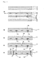
- Fig. 3 (a) to (e) are schematic cross-section views illustrating the flow of manufacture of the ceramic board for semiconductor manufacture apparatuses in Example 1.
- Fig. 4 is a diagrammatic representation of the surface flatness of the ceramic board for semiconductor manufacture apparatuses as fabricated in Example 1.
- Fig. 5 is a diagrammatic representation of the surface flatness of the ceramic board for semiconductor manufacture apparatuses as fabricated in Example 2.
- Fig. 6 (a) to (d) are schematic cross-section views illustrating the flow of manufacture of the ceramic board for semiconductor manufacture apparatuses in Example 3.
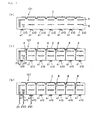
- Fig. 7 (e) to (g) are schematic cross-section views illustrating the flow of manufacture of the ceramic board for semiconductor manufacture apparatuses in Example 3.
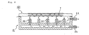
- Fig. 8 is a schematic section view showing the ceramic board obtained in Example 3 as mounted on a support base.
- the ceramic board for semiconductor manufacture apparatuses comprises a ceramic substrate having a surface on which a semiconductor wafer is to be directly mounted or indirectly supported at a fixed distance from said surface, in which the degree of flatness of said surface of the ceramic substrate on which a semiconductor wafer is to be directly mounted or indirectly supported (hereinafter referred to sometimes as wafer-mounting surface) is 1 to 50 ⁇ m over a measurement range of [(diametric end-to-end length) - 10 mm].
- the ceramic board according to the second aspect of the present invention comprises a ceramic substrate and a conductor layer disposed internally or on a surface of said ceramic substrate, in which the degree of flatness of said surface of the ceramic substrate on which a semiconductor wafer is to be directly mounted or indirectly supported is 1 to 50 ⁇ m over a measurement range of [(diametric end-to-end length) - 10 mm].
- the wafer-mounting surface of the ceramic substrate is controlled to a flatness value within a specified range as mentioned above. Therefore, with a hot plate, electrostatic chuck or the like manufactured using either ceramic board as the constituent material, the silicon wafer can be heated uniformly throughout to prevent the breakage of the wafer by thermal shock and, at the same time, can be attracted with a sufficient force of attraction and set securely in position.
- the span of said clearance can be made substantially uniform so that the uneven distribution of wafer temperature can be prevented.
- the ceramic board according to the first aspect of the invention is different from the ceramic board according to the second aspect of the invention only in the restriction on conductor layer and otherwise is identical in construction to the latter ceramic board. Therefore, in the following description of the ceramic boards according to the first and second aspect of the invention, both boards will be collectively referred to as the ceramic board except in cases in which a distinction must be made between the two boards.
- the mode of application of the ceramic board of the invention is not restricted to the application in which a silicon wafer is mounted directly or indirectly thereon for various kinds of processing (for example, formation of circuits).
- the ceramic board for semiconductor manufacture apparatuses according to the present invention is not restricted to any particular kind insofar as it is used for the manufacture of implements for semiconductor manufacture apparatuses, but includes the electrostatic chuck, wafer prover, susceptor, and hot plate (ceramic heater).
- the implements as so referred to in this specification include instruments to be used in the inspection stage.
- the ceramic board for semiconductor manufacture apparatuses according to the invention as a ceramic heater, if the flatness of said wafer-mounting surface exceeds 50 to m over a measurement range of [(diametric end-to-end length) - 10 mm], the wafer temperature will not increase sufficiently regardless of whether the wafer is directly mounted or supported at a fixed distance from the wafer-mounting surface.
- the wafer even if it is attempted to heat the wafer mounted on such a ceramic board, the wafer will not be heated to a temperature of, say, 200 °C because its contact with the ceramic board is either point contact or line contact.
- the wafer supported with pins at a fixed distance from the surface of such a ceramic board even if it is attempted to heat the wafer supported with pins at a fixed distance from the surface of such a ceramic board, the excessive variation in the clearance between the wafer and the heating surface of the ceramic board will bring the wafer into local contact with the ceramic board, with the result that the wafer cannot be properly heated.
- the flatness value of the wafer-mounting surface of the ceramic board is greater than 20 ⁇ m over a measurement range of [(diametric end-to-end length) - 10 mm]
- a gap will be formed between the silicon wafer and the wafer-mounting surface so that a large temperature gradient is at times produced in the wafer.
- the excessively large variation in distance between the silicon wafer and the wafer-mounting surface of the ceramic substrate similarly produces a temperature gradient in the wafer at times.
- said flatness value is greater than 50 ⁇ m in the mode of use of the ceramic board for semiconductor manufacture apparatuses (hereinafter referred to briefly as ceramic board) as a wafer prover, gaps will be created between the silicon wafer mounted and the surface of the ceramic substrate, and when the tester pin is depressed in the area corresponding to such a gap, the silicon wafer deforms in conformity with the surface undulation of the ceramic board and becomes damaged.
- the preferred value of said flatness is 1 to 20 ⁇ m.
- the wafer prover is an instrument for use in a conduction test which comprises pressing tester pins against a silicon wafer placed thereon.
- the shape of said nitride ceramic substrate is not particularly restricted but may for example be elliptic in plan view but a circular board or disk is preferred.
- the nitride ceramic board is a disk, its diameter is preferably over 150 mm, more preferably over 200 mm, and still more preferably over 300 mm. This is because the diameters of semiconductor wafers in popular use today are not less than 8 inches (200 mm) and the next-generation semiconductor wafers will mostly be available in the diameter range of not less than 12 inches (300 mm).
- the compatible wafer will also be so small in diameter that it will be readily heated uniformly and even if the flatness value of the ceramic substrate is large, the wafer will be ready to follow the surface topology of the ceramic substrate so that no reduction in chucking force will take place.
- a ceramic substrate does not have the problems to be solved by the present invention.
- the effect of the present invention is particularly remarkable when the ceramic board diameter is not less than 200 mm.
- the thickness of said ceramic board is preferably not over 50 mm, for such aboard does not easily undergo warp at high temperature.
- the more preferred thickness is less than 8 mm. This is because, when the board thickness is 8 mm or greater, the heat capacity of the ceramic board is increased so that when the heating and cooling cycle is controlled with a temperature control means, the temperature follow-up efficiency is adversely affected.
- the thickness of the ceramic substrate is more preferably not greater than 5 mm. If the thickness exceeds 5 mm, the heat capacity of the substrate will be increased to adversely affect temperature controllability and temperature uniformity of the wafer-mounting surface at times.
- ceramics having a Young's modulus of not less than 280 GPa over the temperature range of room temperature to 800 °C are not particularly restricted but include nitride ceramics, among others. If Young's modulus is less than 280 GPa, the amount of warp at high temperature will be too large to be controlled even if a reinforcing conductive layer is provided.
- nitride ceramics mentioned above may be any of aluminum nitride, silicon nitride, boron nitride and other ceramics but the use of aluminum nitride is preferred.
- the most preferred is a ceramic board comprising aluminum nitride of more than 50 weight %.
- the other ceramic components which can be used include alumina sialon, and the like.
- the Young's modulus of said ceramic substrate can be controlled by using a blend or a laminate of two or more different ceramics or incorporating oxides of metals, such as alkali metals, alkaline earth metals, and rare earth metals, carbon, etc.
- the preferred alkali metals or alkaline earth metals are Li, Na, Ca and Rb, and the preferred rare earth metal is Y.
- the carbon may be whichever of amorphous carbon and crystalline carbon.
- the carbon content is preferably 200 to 5000 ppm. By using carbon within this range, the ceramic board can be blackened.
- the ceramic board of the present invention preferably has no porosity, i.e. 0%, or a porosity of not over 5%.
- porosity i.e. 0%
- the maximum pore diameter of the ceramic substrate is preferably 0 or not more than 50 ⁇ m.
- the pore size is 0 or not more than 50 ⁇ m, the board does not warp even at 200 °C or up and the flatness at room temperature can be maintained at high temperature.
- the porosity mentioned above is measured by the method of Archimedes. To measure the maximum pore diameter, 5 samples are prepared and respectively photographed in 10 positions under an electron microscope and the diameters of the largest pores (50 pores) in each shot are averaged.
- the conductor layer When a conductor layer is to be formed internally or on a surface of said ceramic substrate, the conductor layer preferably comprises a metal or conductive ceramic paste, and at least a single layer is preferably disposed in the center in thickness direction of the ceramic substrate or in an offset position displaced from the center toward the surface opposite to the wafer-mounting surface. As an alternative, the conductor layer may be formed on the surface opposite to the wafer-mounting surface.
- the particular conductor layer is formed on the surface of the ceramic substrate on the side on which a semiconductor wafer is mounted.
- the semiconductor wafer is mounted on this conductor layer.
- the ceramic substrate may be internally formed with a conductor layer functioning as a guard electrode and a ground electrode.
- the conductor layer is to constitute electrodes (static electrodes) of an electrostatic chuck, it is formed internally of the ceramic substrate but closer to the wafer-mounting surface.
- the configuration of said conductor layer may for example be a plane, several divisions of a plane, a vortex, concentric circles, or a grid.
- the thickness of said conductor layer is preferably about 1 to 50 ⁇ m. If the layer is less than 1 ⁇ m thick, no reinforcing effect will be obtained. If the thickness is greater than 50 ⁇ m, warp of the whole ceramic board and a reduction in flatness of the wafer-mounting surface will be induced.
- the conductor layer may for example be comprised of a sintered metal, non-sintered metal, or a sintered conductive ceramic material.
- the raw material of said sintered metal or non-sintered metal may for example be a high-melting metal.
- the high-melting metal mentioned just above includes tungsten, molybdenum, nickel and indium. These metals may be used singly or in a combination of two or more species.
- the conductive ceramic material mentioned above includes the carbide of tungsten or molybdenum.
- the conductor layer when it is formed internally of the ceramic substrate, may be utilized as, for example, a heating element, a guard electrode, a ground electrode and/or static electrodes and, when it is formed on the surface of the ceramic substrate, can be utilized as, for example, a heating element or chuck top electrodes.
- the ceramic substrate may be internally formed with a plurality of conductor layers adapted to function as, for example, a heating element, a guard electrode, a ground electrode, etc., respectively.
- the ceramic board provided with a heating element and others in this manner can be used as, for example, a hot plate (ceramic heater), an electrostatic chuck, or a wafer prover.
- Fig. 1 is a schematic bottom view of a ceramic heater as an application of the ceramic board for semiconductor manufacture apparatuses according to the present invention and Fig. 2 is a schematic partial section view, on exaggerated scale, of the same ceramic heater.
- a ceramic substrate 11 is provided in the form of a disk and a conductor layer (heating element) 12 is formed in a pattern of concentric circles on the bottom surface of said ceramic substrate 11 for heating the whole wafer-mounting surface to a uniform temperature.
- the conductor layer 12 pattern comprises a plurality of concentric circles with each set of two neighboring circles constituting a single conductor line which is connected, at ends, to an input and an output terminal pin 13.
- through holes 15 are formed for accepting support pins 16.
- blind holes 14a to 14i are formed for accepting temperature probes.
- said support pins 16 are adapted to support a silicon wafer 19 and to raise and lower it with respect to the ceramic board surface so that the wafer 19 maybe delivered to a transfer machine (not shown) or received from the like transfer machine.
- the conductor layer 12 as the heating element may be disposed internally in the center in thickness direction of the ceramic substrate 11 or in an offset position displaced from the center toward the wafer-mounting surface.
- the conductor layer 12 functions not only as a mechanical reinforcement but also as a heating element.
- a conductive paste containing a metal or conductive ceramic powder is preferably employed.
- the procedure for constructing a conductor layer internally of the ceramic substrate comprises forming a conductor paste layer on a green sheet, laminating one or more green sheets thereon and baking the laminate.
- the procedure for constructing a conductor layer on the surface generally comprises fabricating a ceramic substrate, forming a conductor paste layer on the surface of the substrate and sintering it.
- the conductor paste mentioned above is not particularly restricted but is preferably a paste containing a resin, a solvent, a thickener, etc. in addition to the metal or conductive ceramic powder necessary for electrical conductivity.
- the preferred metal powder for this purpose includes powders of noble metals (gold, silver, platinum, palladium), lead, tungsten, molybdenum and nickel. These may be used alone or in a combination of two or more species. These metals are more or less hardly oxidizable and have sufficient resistance to generate heat.
- the conductive ceramic powder includes a powder of tungsten carbide or molybdenum carbide. These powders can be used singly or in a combination of two or more species.
- the preferred particle diameter of said metal or conductive ceramic powder is 0.1 to 100 ⁇ m. If the powder is finer than 0.1 ⁇ m, it will be ready to be oxidized. On the other hand, if the limit of 100 ⁇ m is exceeded, the powder will not be easily sintered and the resistance value will be increased.
- the metal powder mentioned above may be spherical or flaky.
- a mixture of spherical and flaky powders may also be employed.
- the metal powder comprises flaky particles or a mixture of spherical and flaky particles
- the metal oxide added is held more effectively between the metal particles, with the consequent advantage that a firmer adhesion can be realized between the conductor layer 12 and the nitride ceramics and that the resistance value can be increased.
- the resin for use in the conductor paste includes epoxy resin and phenolic resin.
- the solvent may for example be isopropyl alcohol.
- the thickener may for example be cellulose.
- the conductor paste is preferably a paste prepared by adding metal oxides to the starting metal powder so that the conductor layer 12 will be a sintered body composed of the metal and metal oxide.
- the conductor layer 12 will be a sintered body composed of the metal and metal oxide.
- the metal oxide mentioned above is preferably at least one member selected from the group consisting of lead oxide, zinc oxide, silica, boron oxide (B 2 O 3 ), alumina, yttria and titania.
- These oxides are capable of improving the adhesion between the metal powder and nitride ceramics without increasing the resistance value of the conductor layer 12.
- the proportions of said lead oxide, zinc oxide, silica, boron oxide (B 2 O 3 ), alumina, yttria and titania in each 100 weight parts of the total metal oxide are 1 to 10 (weight parts; the same applies below) for lead oxide, 1 to 30 for silica, 5 to 50 for boron oxide, 20 to 70 for zinc oxide, 1 to 10 for alumina, 1 to 50 for yttria, and 1 to 50 for titania.
- the total of these oxides is preferably not more than 100 weight parts.
- the adhesion to nitride ceramics in particular, can be improved.
- the addition amount of said metal oxide relative to the metal powder is preferably not less than 0.1 weight % and less than 10 weight %.
- the area resistivity of a conductor layer 12 formed from a conductor paste of such composition is preferably 1 to 45 m ⁇ / ⁇ .
- the area resistivity exceeds 45 m ⁇ / ⁇ , the generation of heat will be too great in relation to the level of voltage applied so that the amount of heat can hardly be controlled in the case of a ceramic substrate 11 carrying the conductor layer 12 on the surface. If the addition amount of said metal oxide exceeds 10 weight %, the area resistivity will exceed 50 m ⁇ / ⁇ , so that the excessively increased heat generation makes temperature control difficult and the uniformity of temperature distribution will be sacrificed.
- the surface of the conductor layer 12 is preferably provided with a metal cover layer 17 as illustrated in Fig. 2 for preventing oxidation of the sintered metal and consequent change in resistance value.
- the thickness of the metal cover layer thus formed is preferably 0.1 to 10 ⁇ m.
- the metal for use in the formation of said metal cover layer is not particularly restricted only provided that it is a non-oxidizable metal but may for example be gold, silver, palladium, platinum or nickel. These metals can be used alone or in a combination of two or more species. Among the metals mentioned above, nickel is particularly preferred.
- thermocouples may be embedded in the ceramic board. This is because by measuring the temperature of the heating element with the thermocouples and varying the voltage and current values based on the temperature data, the heater temperature can be controlled.
- the size of junctions of the conductors of the thermocouple is preferably equal to the diameter of each conductor or larger but not larger than 0.5 mm.
- thermocouple As examples of said thermocouple, the K, R, B, S, E, J and T thermocouples as defined in JIS C-1602 (1980) can be mentioned.
- nitride ceramic powder described above e.g. an aluminum nitride ceramic powder
- sintering aids such as yttria, etc.
- binder such as a binder
- This slurry is granulated by the spray-drying method and the resulting granules are placed in a metal mold or the like and compressed into a green board.
- the green board is optionally formed with through holes 15 for accepting the support pins 16 for supporting a silicon wafer and with blind holes 14a to 14i in which temperature probes such as thermocouples are to be embedded.
- this green board is sintered by heating to provide a blank ceramic board.
- a ceramic substrate 11 is then prepared by machining this ceramic board to predetermined shape.
- the board may be formed to the specified size so that it may directly serve as a ceramic substrate 11.
- the heating temperature may be any temperature not below the sintering point but, in the case of nitride ceramics, the range of 1000 to 2500 °C is used.
- the flatness is adjusted after sintering.
- the desired flatness can be attained by grinding both sides simultaneously using a #100 to #800 (grit size) diamond wheel (two-sided wheel) while a pressure of 0.1 to 50 kg/cm 2 is applied.
- the rotational speed of the diamond wheel is 50 to 300 rpm.
- the diamond wheel is prepared by electrodeposition of diamond.
- the conductor paste is generally a highly viscous fluid comprising a metal powder, a resin and a solvent.
- the conductor paste layer is formed by printing the substrate in the areas corresponding to the conductor layer with said conductor paste by the screen printing technique, for instance. Since the conductor layer is required to heat the ceramic substrate uniformly over its whole surface, it is preferably printed in a concentric circular pattern as illustrated in Fig. 1.
- the conductor paste layer be formed in such a manner that the conductor layer 12 after baking will present a rectangular section and a flat surface.
- the conductor paste layer formed on the bottom surface of the ceramic substrate 11 is then heated and sitered to remove the resin and solvent and bake the metal powder onto the bottom surface of the ceramic substrate 11 to complete a conductor layer 12.
- the heating temperature is preferably 500 to 1000 °C.
- the metal powder, ceramic substrate and metal oxide are integrally sintered to provide an improved bond between the conductor layer and ceramic substrate.
- the surface of the conductor layer 12 is preferably provided with the metal cover layer.
- the metal cover layer can be formed by, for example, electrolytic plating, electroless plating or sputtering but, for mass production, electroless plating is the most suitable method.
- thermocouples are set in the blind holes 14a to 14i and sealed with a ceramic and a heat-resistant resin such as a polyimide resin to complete the manufacture of a ceramic board having a conductor layer on the bottom side.
- the nitride ceramic powder is mixed with the binder, solvent, etc. to prepare a paste, and using the paste, a green sheet is formed.
- the ceramic powder which can be used includes an aluminum nitride powder, and where necessary, sintering aids such as yttria may be added.
- the binder is preferably at least one member selected from the group consisting of acrylic binder, ethylcellulose, butylcellosolve and polyvinyl alcohol.
- the solvent is preferably at least one member selected from the group consisting of ⁇ -terpineol and glycol.
- the paste obtained by compounding those components is molded by the doctor blade method to provide said green sheet.
- the preferred thickness of the green sheet is 0.1 to 5 mm.
- the green sheet is formed with means to serve as through holes for accepting support pins for supporting a silicon wafer, means to serve as blind holes in which temperature probes such as thermocouples are to be embedded, and means for serving as plated-through holes for connecting the conductor layer to external terminal pins.
- This processing may be carried out after formation of a green sheet laminate to be described below.
- the conductive paste containing a metal or conductive ceramic powder is printed.
- the conductive paste contains a metal or conductive ceramic powder.
- the mean particle diameter of tungsten or molybdenum powder is preferably 0.1 to 5 ⁇ m. If the mean particle diameter is less than 0.1 ⁇ m or over 5 ⁇ m, the conductive paste will hardly be printed.
- the conductive paste may for example be a composition (paste) composed of 85 to 87 weight parts of a metal or conductive ceramic powder, 1.5 to 10 weight parts of at least one kind of binder selected from the group consisting of acrylic binder, ethylcellulose, butylcellosolve and polyvinyl alcohol, and at least one kind of solvent selected from the group consisting of ⁇ -terpineol and glycol.
- a composition composed of 85 to 87 weight parts of a metal or conductive ceramic powder, 1.5 to 10 weight parts of at least one kind of binder selected from the group consisting of acrylic binder, ethylcellulose, butylcellosolve and polyvinyl alcohol, and at least one kind of solvent selected from the group consisting of ⁇ -terpineol and glycol.
- the green sheets not printed with the conductive paste are laminated on both sides of the green sheet printed with the conductive paste.
- this step it is arranged so that the number of green sheets to be laminated on the top side is larger than the number of green sheets to be laminated on the bottom side so that the conductor layer will be situated offset in the direction of the bottom side.
- the preferred number of green sheets laminated is 20 to 50 on the top side and 5 to 20 on the bottom side.
- the green sheet laminate is hot-pressed to sinter the green sheets and the conductive paste within the laminate.
- the heating temperature is preferably 1000 to 2000 °C and the pressure to be applied is preferably 100 to 200 kg/cm 2 .
- the heating is performed in an inert gas atmosphere.
- the inert gas may for example be argon gas or nitrogen gas.
- the blind holes for accepting temperature probes may be formed after this sintering operation.
- the blind holes can be formed by blasting, e.g. sandblasting, after surface grinding.
- terminals are connected to the plated-through holes for electrical connection to the internal conductor layer, followed by heating for reflow.
- the heating temperature is preferably 200 to 500 °C.
- the flatness is adjusted after sintering.
- the desired flatness can be attained by grinding both sides simultaneously using a #100 to #800 (grit size) diamond wheel (two-sided wheel) while a pressure of 0.1 to 50 kg/cm 2 is applied.
- the rotational speed of the diamond wheel is 50 to 300 rpm.
- the diamond wheel is prepared by electrodeposition of diamond.
- thermocouples as temperature probes are sealed with a heat-resistant resin to complete a ceramic board internally provided with a conductor layer.
- Example 1 Manufacture of a ceramic board internally provided with a conductor layer
- Test Example 1 Manufacture of a ceramic board internally provided with a conductor layer
- Example 1 Except that diamond grinding was not performed, the procedure of Example 1 was otherwise repeated to provide a ceramic board.
- the flatness of the wafer-mounting surface of this ceramic board was 25.5 ⁇ m in the X-direction and 23.4 ⁇ m in the Y-direction over the measurement length of 205 mm.
- Comparative Example 1 Manufacture of a ceramic board internally provided with a conductor layer
- a ceramic substrate was fabricated in the same manner as in Example 1 and, then, subjected to the following diamond grinding.
- the flatness of the wafer-mounting surface of the resulting ceramic board was 0.55 ⁇ m in the X-direction and 0.84 ⁇ m in the Y-direction over a measurement range of 205 mm.
- Example 1 Except that the diameter of the substrate was set to 190 mm and the substrate was not ground, the procedure of Example 1 was otherwise repeated to provide a ceramic board.
- the flatness of the wafer-mounting surface of this ceramic board was 25 ⁇ m in the X-direction and 23 ⁇ m in the Y-direction over a measurement range of 180 mm.
- Example 1 Except that a ceramic disk to be rejected after hot-pressing was used, the procedure of Example 1 was otherwise repeated to provide a ceramic board.
- the flatness of the wafer-mounting surface of this ceramic board was 55 ⁇ m in the X-direction and 52 ⁇ m in the Y-direction over a measurement range of 205 mm.
- Example 2 Manufacture of a ceramic board provided with a conductor layer on the surface
- Example 2 Except that a ceramic disk rejected after hot-pressing was used and no diamond grinding was performed, the procedure of Example 2 was otherwise repeated to provide a ceramic board.
- the flatness of the wafer-mounting surface of this ceramic board was 55 ⁇ m in the X-direction and 60 ⁇ m in the Y-direction over a measurement length of 205 mm.
- Example 2 Except that only one side of the substrate was ground with a #220 diamond wheel at 100 rpm under no-load (dead load), the procedure of Example 2 was otherwise repeated to provide a ceramic board.
- the flatness of the wafer-mounting surface of this ceramic board was 0.45 ⁇ m in the X-direction and 0.65 ⁇ m in the Y-direction over a measurement length of 205 mm.
- Example 2 Except that no diamond grinding was performed, the procedure of Example 2 was otherwise repeated to provide a ceramic board.
- the flatness of the wafer-mounting surface of this ceramic board was 23 ⁇ m in the X-direction and 22 ⁇ m in the Y-direction over a measurement length of 205 mm.
- Example 2 the temperature difference was 1 °C.
- Comparative Example 3 the wafer could not be held apart by 50 ⁇ m, for the wafer would have contacted the ceramic board.
- Comparative Example 4 the silicon wafer could not be released from the ceramic board.
- the temperature difference of the wafer was 5 °C .
- Test Example 4 Manufacture of an electrostatic chuck
- Example 3 Except that diamond grinding was not performed, the procedure of Example 3 was otherwise repeated to provide an electrostatic chuck.
- the flatness of the wafer-mounting (heating) surface of this electrostatic chuck was 25.5 ⁇ m in the X-direction and 23.4 ⁇ m in the Y-direction over a measurement range of 205 mm.
- An aluminum nitride board was prepared as in Example 3 and ground with a diamond wheel as in Comparative Example 1 to provide an electrostatic chuck.
- the flatness of the wafer-mounting surface of this electrostatic chuck was 0.55 ⁇ m in the X-direction and 0.84 ⁇ m in the Y-direction over a measurement range of 205 mm.
- Example 3 Except that the diameter of the ceramic disk was set to 190 mm and the disk was not ground, the procedure of Example 3 was otherwise repeated to provide an electrostatic chuck.
- the flatness of the wafer-mounting (heating) surface of this electrostatic chuck was 26 ⁇ m in the X-direction and 25 ⁇ m in the Y-direction over a measurement range of 180 mm.
- Example 3 Except that a ceramic board rejected after hot-pressing was used, the procedure of Example 3 was otherwise repeated to provide an electrostatic chuck.
- the flatness of the wafer-mounting (heating) surface of this electrostatic chuck was 55 ⁇ m in the X-direction and 52 ⁇ m in the Y-direction over a measurement range of 205 mm.
- the releasing force required in a vacuum was 125 g/cm 2 in the case of the electrostatic chuck according to Example 3 and 80 g/cm 2 in the case of the electrostatic chuck according to Test Example 4.
- the silicon wafer became unreleasable when the atmospheric pressure was reinstated and, when forced to release it, the wafer was damaged.
- the releasing force required was 110 kg/cm 2 .
- the wafer cracked when a voltage of 1 kV was applied to the chuck to measure the force of attraction.
- Test Example 6 Manufacture of a wafer prover
- Example 4 Except that diamond grinding was not performed, the procedure of Example 4 was otherwise repeated to provide a wafer prover.
- the flatness of the wafer-mounting surface of this wafer prover was 25.5 ⁇ m in the X-direction and 23.4 ⁇ m in the Y-direction over a measurement range of 205 mm.
- Example 4 Except that a ceramic substrate rejected after hot-pressing was used, the procedure of Example 4 was otherwise repeated to provide a wafer prover.
- the flatness of the wafer-mounting surface of this wafer prover was 55 ⁇ m in the X-direction and 52 ⁇ m in the Y-direction over a measurement range of 205 mm.
- a silicon wafer was mounted on each of the wafer provers obtained in Example 4 and Test Example 6 and heated. With the wafer prover according to Example 4, the silicon wafer was not damaged. With the wafer prover according to Test Example 6, the wafer was destroyed.
- a silicon wafer was mounted on the wafer prover obtained in Comparative Example 7 and the temperature was increased to 200 °C. However, because the wafer and the prover were in line contact, the wafer temperature failed to rise and the test could not be performed.
- a silicon wafer can be successfully heated.
- a uniform wafer temperature can be obtained by controlling the flatness to not more than 20 ⁇ m.
- chucking the work causes no wafer damage.
- the ceramic board for semiconductor manufacture apparatuses according to the present invention when used as a heater, heats a silicon wafer uniformly throughout and, hence, does not damage the wafer and, when used as an electrostatic chuck, provides a sufficient chucking force, thus finding application as implements for semiconductor manufacture apparatuses, such as the hot plate, electrostatic chuck and wafer prover, with the outstanding advantage.
Landscapes
- Container, Conveyance, Adherence, Positioning, Of Wafer (AREA)
- Surface Heating Bodies (AREA)
- Resistance Heating (AREA)
Applications Claiming Priority (3)
| Application Number | Priority Date | Filing Date | Title |
|---|---|---|---|
| JP22676899 | 1999-08-10 | ||
| JP22676899 | 1999-08-10 | ||
| PCT/JP1999/007368 WO2001013423A1 (en) | 1999-08-10 | 1999-12-28 | Semiconductor production device ceramic plate |
Publications (2)
| Publication Number | Publication Date |
|---|---|
| EP1120829A1 true EP1120829A1 (de) | 2001-08-01 |
| EP1120829A4 EP1120829A4 (de) | 2009-05-27 |
Family
ID=16850318
Family Applications (1)
| Application Number | Title | Priority Date | Filing Date |
|---|---|---|---|
| EP99961446A Withdrawn EP1120829A4 (de) | 1999-08-10 | 1999-12-28 | Keramische platte für halbleiterproduktionsanordnung |
Country Status (3)
| Country | Link |
|---|---|
| US (4) | US6717116B1 (de) |
| EP (1) | EP1120829A4 (de) |
| WO (1) | WO2001013423A1 (de) |
Families Citing this family (40)
| Publication number | Priority date | Publication date | Assignee | Title |
|---|---|---|---|---|
| US6717116B1 (en) * | 1999-08-10 | 2004-04-06 | Ibiden Co., Ltd. | Semiconductor production device ceramic plate |
| US6900149B1 (en) * | 1999-09-06 | 2005-05-31 | Ibiden Co., Ltd. | Carbon-containing aluminum nitride sintered compact and ceramic substrate for use in equipment for manufacturing or inspecting semiconductor |
| JP2001237053A (ja) * | 1999-12-14 | 2001-08-31 | Ibiden Co Ltd | 半導体製造・検査装置用セラミックヒータおよび支持ピン |
| US20040222211A1 (en) * | 1999-12-28 | 2004-11-11 | Ibiden Co., Ltd. | Carbon-containing aluminum nitride sintered body, and ceramic substrate for a semiconductor producing/examining device |
| WO2001062686A1 (en) * | 2000-02-24 | 2001-08-30 | Ibiden Co., Ltd. | Aluminum nitride sintered compact, ceramic substrate, ceramic heater and electrostatic chuck |
| JP2001247382A (ja) * | 2000-03-06 | 2001-09-11 | Ibiden Co Ltd | セラミック基板 |
| WO2001066488A1 (en) | 2000-03-07 | 2001-09-13 | Ibiden Co., Ltd. | Ceramic substrate for manufacture/inspection of semiconductor |
| US20040074586A1 (en) * | 2000-03-15 | 2004-04-22 | Yasuji Hiramatsu | Method of producing electrostatic chucks and method of producing ceramic heaters |
| EP1233651A1 (de) * | 2000-04-07 | 2002-08-21 | Ibiden Co., Ltd. | Keramisches heizelement |
| JP3565496B2 (ja) * | 2000-04-13 | 2004-09-15 | イビデン株式会社 | セラミックヒータ、静電チャックおよびウエハプローバ |
| US7071551B2 (en) * | 2000-05-26 | 2006-07-04 | Ibiden Co., Ltd. | Device used to produce or examine semiconductors |
| JP3516392B2 (ja) * | 2000-06-16 | 2004-04-05 | イビデン株式会社 | 半導体製造・検査装置用ホットプレート |
| WO2002003435A1 (en) * | 2000-07-04 | 2002-01-10 | Ibiden Co., Ltd. | Hot plate for semiconductor manufacture and testing |
| WO2002009171A1 (en) * | 2000-07-25 | 2002-01-31 | Ibiden Co., Ltd. | Ceramic substrate for semiconductor manufacture/inspection apparatus, ceramic heater, electrostatic clampless holder, and substrate for wafer prober |
| JP2002160974A (ja) * | 2000-11-22 | 2002-06-04 | Ibiden Co Ltd | 窒化アルミニウム焼結体、窒化アルミニウム焼結体の製造方法、セラミック基板およびセラミック基板の製造方法 |
| US20040206747A1 (en) * | 2001-04-11 | 2004-10-21 | Yasutaka Ito | Ceramic heater for semiconductor manufacturing/inspecting apparatus |
| JP3753040B2 (ja) * | 2001-09-25 | 2006-03-08 | 住友電気工業株式会社 | 光ファイバ融着接続部の加熱方法および加熱装置 |
| US7234117B2 (en) * | 2002-08-28 | 2007-06-19 | Microsoft Corporation | System and method for shared integrated online social interaction |
| JP3975944B2 (ja) * | 2003-02-27 | 2007-09-12 | 住友電気工業株式会社 | 半導体あるいは液晶製造装置用保持体およびそれを搭載した半導体あるいは液晶製造装置 |
| US7709814B2 (en) * | 2004-06-18 | 2010-05-04 | Axcelis Technologies, Inc. | Apparatus and process for treating dielectric materials |
| TWI353631B (en) * | 2004-06-28 | 2011-12-01 | Kyocera Corp | Wafer heating device and semiconductor equipment |
| US20060088692A1 (en) * | 2004-10-22 | 2006-04-27 | Ibiden Co., Ltd. | Ceramic plate for a semiconductor producing/examining device |
| US7300707B2 (en) * | 2004-10-25 | 2007-11-27 | Creative Technology Corporation | Aluminium composite structure having a channel therein and method of manufacturing the same |
| US20070044916A1 (en) * | 2005-08-31 | 2007-03-01 | Masakazu Isozaki | Vacuum processing system |
| EP1795498A3 (de) * | 2005-12-06 | 2011-05-11 | Yamaha Corporation | Verpackung für eine Halbleitervorrichtung |
| JP4827569B2 (ja) * | 2006-03-23 | 2011-11-30 | 大日本スクリーン製造株式会社 | 基板支持構造とこれを用いた熱処理装置と基板支持構造に用いられるシート状物と基板支持構造の製造方法 |
| US8226769B2 (en) * | 2006-04-27 | 2012-07-24 | Applied Materials, Inc. | Substrate support with electrostatic chuck having dual temperature zones |
| JP2008108703A (ja) * | 2006-09-28 | 2008-05-08 | Covalent Materials Corp | 面状ヒータ及びこのヒータを備えた半導体熱処理装置 |
| JP5117146B2 (ja) * | 2006-12-15 | 2013-01-09 | 日本碍子株式会社 | 加熱装置 |
| US7763831B2 (en) * | 2006-12-15 | 2010-07-27 | Ngk Insulators, Ltd. | Heating device |
| US7777160B2 (en) * | 2007-12-17 | 2010-08-17 | Momentive Performance Materials Inc. | Electrode tuning method and apparatus for a layered heater structure |
| WO2010090948A1 (en) * | 2009-02-04 | 2010-08-12 | Mattson Technology, Inc. | Electrostatic chuck system and process for radially tuning the temperature profile across the surface of a substrate |
| US8580593B2 (en) * | 2009-09-10 | 2013-11-12 | Micron Technology, Inc. | Epitaxial formation structures and associated methods of manufacturing solid state lighting devices |
| US9538583B2 (en) * | 2013-01-16 | 2017-01-03 | Applied Materials, Inc. | Substrate support with switchable multizone heater |
| US10636690B2 (en) * | 2016-07-20 | 2020-04-28 | Applied Materials, Inc. | Laminated top plate of a workpiece carrier in micromechanical and semiconductor processing |
| KR102339550B1 (ko) * | 2017-06-30 | 2021-12-17 | 주식회사 미코세라믹스 | 질화 알루미늄 소결체 및 이를 포함하는 반도체 제조 장치용 부재 |
| JP7122174B2 (ja) * | 2018-06-25 | 2022-08-19 | 日本特殊陶業株式会社 | 静電チャック、および、静電チャックの製造方法 |
| JP7175323B2 (ja) * | 2018-09-28 | 2022-11-18 | 京セラ株式会社 | セラミック構造体及びウェハ用システム |
| US12451338B2 (en) * | 2021-06-15 | 2025-10-21 | Kyocera Corporation | Plasma treatment apparatus member |
| CN118147615A (zh) * | 2022-12-06 | 2024-06-07 | 中微半导体设备(上海)股份有限公司 | 分气转接环、托盘旋转机构及半导体处理设备 |
Family Cites Families (60)
| Publication number | Priority date | Publication date | Assignee | Title |
|---|---|---|---|---|
| US6635853B2 (en) * | 1909-08-09 | 2003-10-21 | Ibiden Co., Ltd. | Hot plate unit |
| US4804823A (en) * | 1986-07-31 | 1989-02-14 | Kyocera Corporation | Ceramic heater |
| JP2511295B2 (ja) | 1988-07-26 | 1996-06-26 | 富士写真フイルム株式会社 | マイクロフィルム撮影用ロ―タリ―カメラ |
| JPH02174116A (ja) | 1988-12-26 | 1990-07-05 | Toshiba Ceramics Co Ltd | サセプタ |
| US5151871A (en) * | 1989-06-16 | 1992-09-29 | Tokyo Electron Limited | Method for heat-processing semiconductor device and apparatus for the same |
| EP0447155B1 (de) | 1990-03-12 | 1995-07-26 | Ngk Insulators, Ltd. | Wafer-Heizgeräte für Apparate, zur Halbleiterherstellung Heizanlage mit diesen Heizgeräten und Herstellung von Heizgeräten |
| JPH0628258B2 (ja) | 1990-07-20 | 1994-04-13 | 日本碍子株式会社 | 半導体ウエハー加熱装置及びその製造方法 |
| US5280156A (en) * | 1990-12-25 | 1994-01-18 | Ngk Insulators, Ltd. | Wafer heating apparatus and with ceramic substrate and dielectric layer having electrostatic chucking means |
| JPH04287344A (ja) | 1991-03-15 | 1992-10-12 | Kyocera Corp | 静電チャックの接合構造 |
| JPH06291049A (ja) | 1993-03-31 | 1994-10-18 | Kyocera Corp | 薄膜形成装置 |
| JPH07183342A (ja) * | 1993-12-22 | 1995-07-21 | Nippon Telegr & Teleph Corp <Ntt> | 試料・探針間導通状態判知法 |
| US5463526A (en) * | 1994-01-21 | 1995-10-31 | Lam Research Corporation | Hybrid electrostatic chuck |
| JPH07297265A (ja) | 1994-04-26 | 1995-11-10 | Shin Etsu Chem Co Ltd | 静電チャック |
| JPH0866071A (ja) * | 1994-08-19 | 1996-03-08 | Sony Corp | 静電吸着装置 |
| TW444922U (en) * | 1994-09-29 | 2001-07-01 | Tokyo Electron Ltd | Heating device and the processing device using the same |
| US6133557A (en) * | 1995-01-31 | 2000-10-17 | Kyocera Corporation | Wafer holding member |
| US5886863A (en) * | 1995-05-09 | 1999-03-23 | Kyocera Corporation | Wafer support member |
| US6686191B1 (en) * | 1995-09-22 | 2004-02-03 | Bayer Healthcare Llc | Preparation of virally inactivated intravenously injectable immune serum globulin |
| KR100250636B1 (ko) * | 1996-11-13 | 2000-05-01 | 윤종용 | 반도체 장치 제조용 가열챔버의 원형 가열판 |
| DE59813206D1 (de) * | 1997-01-10 | 2005-12-29 | Ego Elektro Geraetebau Gmbh | Kochsystem mit einer Kontaktwärme übertragenden Elektro-Kochplatte |
| JPH10275524A (ja) | 1997-03-31 | 1998-10-13 | Kyocera Corp | 耐プラズマ部材 |
| JPH10289944A (ja) * | 1997-04-16 | 1998-10-27 | Sony Corp | 静電吸着装置及び静電吸着方法 |
| JP3670444B2 (ja) * | 1997-06-06 | 2005-07-13 | 日本碍子株式会社 | 窒化アルミニウム基複合体、電子機能材料、静電チャックおよび窒化アルミニウム基複合体の製造方法 |
| JP3165396B2 (ja) | 1997-07-19 | 2001-05-14 | イビデン株式会社 | ヒーターおよびその製造方法 |
| JP3145664B2 (ja) | 1997-08-29 | 2001-03-12 | 京セラ株式会社 | ウエハ加熱装置 |
| JP3847920B2 (ja) | 1997-10-06 | 2006-11-22 | 株式会社アルバック | 静電吸着ホットプレート、真空処理装置、及び真空処理方法 |
| JPH11111809A (ja) * | 1997-10-07 | 1999-04-23 | Innotech Corp | 搬送装置 |
| JPH11168134A (ja) * | 1997-12-03 | 1999-06-22 | Shin Etsu Chem Co Ltd | 静電吸着装置およびその製造方法 |
| JP3477062B2 (ja) * | 1997-12-26 | 2003-12-10 | 京セラ株式会社 | ウエハ加熱装置 |
| WO2000069219A1 (en) * | 1999-05-07 | 2000-11-16 | Ibiden Co., Ltd. | Hot plate and method of producing the same |
| JP2001118664A (ja) | 1999-08-09 | 2001-04-27 | Ibiden Co Ltd | セラミックヒータ |
| US6717116B1 (en) * | 1999-08-10 | 2004-04-06 | Ibiden Co., Ltd. | Semiconductor production device ceramic plate |
| EP1199908A4 (de) * | 1999-10-22 | 2003-01-22 | Ibiden Co Ltd | Keramisches heizelement |
| US6632512B1 (en) * | 1999-11-10 | 2003-10-14 | Ibiden Co., Ltd. | Ceramic substrate |
| ATE301916T1 (de) * | 1999-11-19 | 2005-08-15 | Ibiden Co Ltd | Keramisches heizgerät |
| JP2001297857A (ja) * | 1999-11-24 | 2001-10-26 | Ibiden Co Ltd | 半導体製造・検査装置用セラミックヒータ |
| WO2001041508A1 (en) * | 1999-11-30 | 2001-06-07 | Ibiden Co., Ltd. | Ceramic heater |
| EP1383167A1 (de) * | 1999-12-09 | 2004-01-21 | Ibiden Co., Ltd. | Keramische scheibe für ein halbleitererzeugungs/inspektionsgerät |
| US20040222211A1 (en) * | 1999-12-28 | 2004-11-11 | Ibiden Co., Ltd. | Carbon-containing aluminum nitride sintered body, and ceramic substrate for a semiconductor producing/examining device |
| JP3228923B2 (ja) * | 2000-01-18 | 2001-11-12 | イビデン株式会社 | 半導体製造・検査装置用セラミックヒータ |
| JP3228924B2 (ja) * | 2000-01-21 | 2001-11-12 | イビデン株式会社 | 半導体製造・検査装置用セラミックヒータ |
| JP2001244320A (ja) | 2000-02-25 | 2001-09-07 | Ibiden Co Ltd | セラミック基板およびその製造方法 |
| US20040074586A1 (en) * | 2000-03-15 | 2004-04-22 | Yasuji Hiramatsu | Method of producing electrostatic chucks and method of producing ceramic heaters |
| EP1233651A1 (de) * | 2000-04-07 | 2002-08-21 | Ibiden Co., Ltd. | Keramisches heizelement |
| JP2001302330A (ja) * | 2000-04-24 | 2001-10-31 | Ibiden Co Ltd | セラミック基板 |
| EP1225790A1 (de) * | 2000-05-02 | 2002-07-24 | Ibiden Co., Ltd. | Keramisches heizelement |
| WO2001086717A1 (en) * | 2000-05-10 | 2001-11-15 | Ibiden Co., Ltd. | Electrostatic chuck |
| US7071551B2 (en) * | 2000-05-26 | 2006-07-04 | Ibiden Co., Ltd. | Device used to produce or examine semiconductors |
| US6967312B2 (en) * | 2000-07-19 | 2005-11-22 | Ibiden Co., Ltd. | Semiconductor manufacturing/testing ceramic heater, production method for the ceramic heater and production system for the ceramic heater |
| EP1255284A1 (de) * | 2000-07-19 | 2002-11-06 | Ibiden Co., Ltd. | Keramischer heizkörper für die bearbeitung bzw. das testen von halbleitern |
| US6878906B2 (en) * | 2000-08-30 | 2005-04-12 | Ibiden Co., Ltd. | Ceramic heater for semiconductor manufacturing and inspecting equipment |
| JP2002076102A (ja) * | 2000-08-31 | 2002-03-15 | Ibiden Co Ltd | セラミック基板 |
| US20040035846A1 (en) * | 2000-09-13 | 2004-02-26 | Yasuji Hiramatsu | Ceramic heater for semiconductor manufacturing and inspecting equipment |
| JP2002160974A (ja) * | 2000-11-22 | 2002-06-04 | Ibiden Co Ltd | 窒化アルミニウム焼結体、窒化アルミニウム焼結体の製造方法、セラミック基板およびセラミック基板の製造方法 |
| EP1345472A1 (de) * | 2000-11-24 | 2003-09-17 | Ibiden Co., Ltd. | Keramisches heizelement und verfahren zu seiner herstellung |
| US20030000938A1 (en) * | 2000-12-01 | 2003-01-02 | Yanling Zhou | Ceramic heater, and ceramic heater resistor paste |
| WO2002047129A1 (en) * | 2000-12-05 | 2002-06-13 | Ibiden Co., Ltd. | Ceramic substrate for semiconductor manufacturing and inspecting devices, and method of manufacturing the ceramic substrate |
| US6485763B1 (en) * | 2001-05-17 | 2002-11-26 | 2002872 Ontario Limited Inc. | Shelf-stable, spreadable maple syrup composition |
| IL154264A0 (en) * | 2001-06-06 | 2003-09-17 | Ibiden Co Ltd | Wafer prober |
| WO2003015157A1 (en) * | 2001-08-10 | 2003-02-20 | Ibiden Co., Ltd. | Ceramic joint body |
-
1999
- 1999-12-28 US US09/806,477 patent/US6717116B1/en not_active Expired - Lifetime
- 1999-12-28 WO PCT/JP1999/007368 patent/WO2001013423A1/ja not_active Ceased
- 1999-12-28 EP EP99961446A patent/EP1120829A4/de not_active Withdrawn
-
2003
- 2003-01-17 US US10/346,095 patent/US7084376B2/en not_active Expired - Lifetime
- 2003-09-17 US US10/663,681 patent/US20040060919A1/en not_active Abandoned
-
2004
- 2004-05-28 US US10/855,324 patent/US20040217105A1/en not_active Abandoned
Also Published As
| Publication number | Publication date |
|---|---|
| US20040060919A1 (en) | 2004-04-01 |
| US20040217105A1 (en) | 2004-11-04 |
| US20030132217A1 (en) | 2003-07-17 |
| US7084376B2 (en) | 2006-08-01 |
| US6717116B1 (en) | 2004-04-06 |
| EP1120829A4 (de) | 2009-05-27 |
| WO2001013423A1 (en) | 2001-02-22 |
Similar Documents
| Publication | Publication Date | Title |
|---|---|---|
| US6717116B1 (en) | Semiconductor production device ceramic plate | |
| US6639188B2 (en) | Ceramic heater | |
| US7071551B2 (en) | Device used to produce or examine semiconductors | |
| EP1193233A1 (de) | Keramisches substrat zur herstellung von halbleitern/inspektions vorrichtung | |
| KR20020092967A (ko) | 세라믹 기판 및 그 제조 방법 | |
| EP1321971A1 (de) | Keramisches substrat für die halbleiterherstellung und -inspektion | |
| US6884972B2 (en) | Ceramic plate for a semiconductor producing/inspecting apparatus | |
| EP1340732A1 (de) | Aluminiumnitrid-sinterkörper, verfahren zur herstellung von aluminiumnitrid-sinterkörpern, keramisches substrat und verfahren zur herstellung des keramischen substrates. | |
| US20020150789A1 (en) | Ceramic sunstrate | |
| WO2001086717A1 (en) | Electrostatic chuck | |
| US20050153826A1 (en) | Carbon-containing aluminum nitride sintered body, and ceramic substrate for a semiconductor producing/examining device | |
| EP1204298A1 (de) | Keramisches heizelement | |
| JP3565496B2 (ja) | セラミックヒータ、静電チャックおよびウエハプローバ | |
| EP1091400A1 (de) | Testeinrichtung für einen wafer | |
| WO2001078455A1 (fr) | Plaque ceramique | |
| JP3929879B2 (ja) | ウェハ支持部材 | |
| JP2002134600A (ja) | 静電チャック | |
| JP2001319967A (ja) | セラミック基板の製造方法 | |
| JP2001223257A (ja) | 半導体製造・検査装置用セラミック基板 | |
| JP3320706B2 (ja) | ウエハプローバ、ウエハプローバに使用されるセラミック基板およびウエハプローバ装置 | |
| JP2004172637A (ja) | 半導体製造・検査装置用セラミック基板 | |
| JP3971756B2 (ja) | ウェハ加熱装置 | |
| JP2004088117A (ja) | ウエハプローバおよびウエハプローバに使用されるセラミック基板 | |
| JP2005340441A (ja) | ウェハ支持部材 | |
| JPWO2001013423A1 (ja) | 半導体製造装置用セラミック板 |
Legal Events
| Date | Code | Title | Description |
|---|---|---|---|
| PUAI | Public reference made under article 153(3) epc to a published international application that has entered the european phase |
Free format text: ORIGINAL CODE: 0009012 |
|
| 17P | Request for examination filed |
Effective date: 20010308 |
|
| AK | Designated contracting states |
Kind code of ref document: A1 Designated state(s): AT BE CH CY DE DK ES FI FR GB GR IE IT LI LU MC NL PT SE |
|
| A4 | Supplementary search report drawn up and despatched |
Effective date: 20090427 |
|
| STAA | Information on the status of an ep patent application or granted ep patent |
Free format text: STATUS: THE APPLICATION HAS BEEN WITHDRAWN |
|
| 18W | Application withdrawn |
Effective date: 20090602 |