EP1120832A1 - Festkörper -bildaufnahmevovrichtung und herstellungsverfahren - Google Patents
Festkörper -bildaufnahmevovrichtung und herstellungsverfahren Download PDFInfo
- Publication number
- EP1120832A1 EP1120832A1 EP99926920A EP99926920A EP1120832A1 EP 1120832 A1 EP1120832 A1 EP 1120832A1 EP 99926920 A EP99926920 A EP 99926920A EP 99926920 A EP99926920 A EP 99926920A EP 1120832 A1 EP1120832 A1 EP 1120832A1
- Authority
- EP
- European Patent Office
- Prior art keywords
- film
- solid
- state imaging
- imaging device
- reflection film
- Prior art date
- Legal status (The legal status is an assumption and is not a legal conclusion. Google has not performed a legal analysis and makes no representation as to the accuracy of the status listed.)
- Withdrawn
Links
Images




Classifications
-
- H—ELECTRICITY
- H10—SEMICONDUCTOR DEVICES; ELECTRIC SOLID-STATE DEVICES NOT OTHERWISE PROVIDED FOR
- H10F—INORGANIC SEMICONDUCTOR DEVICES SENSITIVE TO INFRARED RADIATION, LIGHT, ELECTROMAGNETIC RADIATION OF SHORTER WAVELENGTH OR CORPUSCULAR RADIATION
- H10F77/00—Constructional details of devices covered by this subclass
- H10F77/30—Coatings
- H10F77/306—Coatings for devices having potential barriers
-
- H—ELECTRICITY
- H10—SEMICONDUCTOR DEVICES; ELECTRIC SOLID-STATE DEVICES NOT OTHERWISE PROVIDED FOR
- H10F—INORGANIC SEMICONDUCTOR DEVICES SENSITIVE TO INFRARED RADIATION, LIGHT, ELECTROMAGNETIC RADIATION OF SHORTER WAVELENGTH OR CORPUSCULAR RADIATION
- H10F39/00—Integrated devices, or assemblies of multiple devices, comprising at least one element covered by group H10F30/00, e.g. radiation detectors comprising photodiode arrays
- H10F39/80—Constructional details of image sensors
- H10F39/805—Coatings
-
- H—ELECTRICITY
- H10—SEMICONDUCTOR DEVICES; ELECTRIC SOLID-STATE DEVICES NOT OTHERWISE PROVIDED FOR
- H10F—INORGANIC SEMICONDUCTOR DEVICES SENSITIVE TO INFRARED RADIATION, LIGHT, ELECTROMAGNETIC RADIATION OF SHORTER WAVELENGTH OR CORPUSCULAR RADIATION
- H10F39/00—Integrated devices, or assemblies of multiple devices, comprising at least one element covered by group H10F30/00, e.g. radiation detectors comprising photodiode arrays
- H10F39/10—Integrated devices
- H10F39/12—Image sensors
- H10F39/18—Complementary metal-oxide-semiconductor [CMOS] image sensors; Photodiode array image sensors
- H10F39/189—X-ray, gamma-ray or corpuscular radiation imagers
-
- H—ELECTRICITY
- H10—SEMICONDUCTOR DEVICES; ELECTRIC SOLID-STATE DEVICES NOT OTHERWISE PROVIDED FOR
- H10F—INORGANIC SEMICONDUCTOR DEVICES SENSITIVE TO INFRARED RADIATION, LIGHT, ELECTROMAGNETIC RADIATION OF SHORTER WAVELENGTH OR CORPUSCULAR RADIATION
- H10F39/00—Integrated devices, or assemblies of multiple devices, comprising at least one element covered by group H10F30/00, e.g. radiation detectors comprising photodiode arrays
- H10F39/80—Constructional details of image sensors
-
- H—ELECTRICITY
- H10—SEMICONDUCTOR DEVICES; ELECTRIC SOLID-STATE DEVICES NOT OTHERWISE PROVIDED FOR
- H10F—INORGANIC SEMICONDUCTOR DEVICES SENSITIVE TO INFRARED RADIATION, LIGHT, ELECTROMAGNETIC RADIATION OF SHORTER WAVELENGTH OR CORPUSCULAR RADIATION
- H10F77/00—Constructional details of devices covered by this subclass
- H10F77/30—Coatings
- H10F77/306—Coatings for devices having potential barriers
- H10F77/331—Coatings for devices having potential barriers for filtering or shielding light, e.g. multicolour filters for photodetectors
- H10F77/334—Coatings for devices having potential barriers for filtering or shielding light, e.g. multicolour filters for photodetectors for shielding light, e.g. light blocking layers or cold shields for infrared detectors
Definitions
- the present invention relates to a solid-state imaging device, and more particularly to a highly sensitive solid-state imaging device that outputs images with an excellent quality and a method for manufacturing the same.
- the solid-state imaging device has the following structure. Photodiodes are formed as light-receiving portions in a semiconductor substrate. Transfer electrodes are formed on this semiconductor substrate via an insulating film. Then, an interlayer insulating film, a shielding film having an opening above the light-receiving portions and a surface protection film are laminated thereon in this order. In such solid-state imaging devices, light enters through the opening of the shielding film and is converted into an electrical charge by the photodiode so as to be accumulated as a signal charge. This signal charge is read out by the CCD and transferred to an output amplifier.
- CCD charge-coupled devices
- the silicon nitride film used as the anti-reflection film in the conventional solid-state imaging devices has a fine crystal structure, causing the following problems. That is, since hydrogen cannot permeate through the silicon nitride film easily, the hydrogen supply to the substrate that is necessary for reducing the dark current is interrupted, making it difficult to improve image quality sufficiently. Also, since the silicon nitride film has a large internal stress, stress concentrates in a stepped portion or the like, causing the problem in that "a white mark," which is a defect in the image quality, is generated easily.
- the solid-state imaging device of the present invention includes a semiconductor substrate, light-receiving portions formed in this semiconductor substrate, and an anti-reflection film formed above this light-receiving portions.
- This anti-reflection film is formed of an oxide having a refractive index of at least 1.9.
- the anti-reflection film is formed of a material having a smaller internal stress than the conventionally used silicon nitride film, there is a smaller stress that is generated in the film to concentrate in the stepped portion. Thus, the defects in the image quality such as a white mark can be reduced. Also, an excellent hydrogen permeability allows a sufficient hydrogen supply to the substrate, which is necessary for reducing the dark current. Moreover, a high refractive index can produce an anti-reflection effect so as to improve the sensitivity.
- the present invention has an advantage in that various designs of the anti-reflection film shapes are possible, thereby further increasing the sensitivity and simplifying the manufacturing process.
- the anti-reflection film is formed of the oxide of at least one metal selected from the group consisting of titanium, zirconium, tantalum, indium and niobium. Also, a preferable thickness of the anti-reflection film is at least 10 nm and not larger than 70 nm. With such structures of the anti-reflection film, it is possible to achieve higher sensitivity of the solid-state imaging device while maintaining the quality of the output images. It is preferable that the anti-reflection film has a refractive index of at least 2.1, and it is particularly preferable that the anti-reflection film has a refractive index of at least 2.3.
- the above solid-state imaging device further includes electrodes for transferring a charge accumulated in the light-receiving portions, a shielding film formed above the electrodes so that an opening is provided above the light-receiving portions, and an interlayer insulating film interposed between the electrodes and the shielding film.
- This interlayer insulating film is formed on the anti-reflection film above the light-receiving portions and has a lower refractive index than the anti-reflection film.
- the interlayer insulating film has a thickness of at least 30 nm and not larger than 600 nm, and it is particularly preferable that the interlayer insulating film has a thickness of at least 30 nm and not larger than 100 nm. With these preferable examples, it is possible to achieve still higher sensitivity of the solid-state imaging device.
- the above solid-state imaging device further includes a surface protection film formed on the interlayer insulating film.
- the surface protection film has a higher refractive index than the interlayer insulating film. It is preferable that this surface protection film has a thickness of at least 100 nm and not larger than 300 nm, and it is particularly preferable that the surface protection film has a thickness of at least 100 nm and not larger than 180 nm. Also, it is preferable that the above solid-state imaging device further includes a silicon oxide film that is interposed between the semiconductor substrate and the anti-reflection film.
- the anti-reflection film is formed so as to cover entirely at least a region where the light-receiving portions are formed, and it is further preferable that the anti-reflection film is formed so as to cover at least a part of a region where electrodes are formed.
- the anti-reflection film is formed so as to cover at least a part of a region where electrodes are formed.
- a method for manufacturing the solid-state imaging device of the present invention includes forming light-receiving portions in a semiconductor substrate, and forming an anti-reflection film above the light-receiving portions.
- the anti-reflection film is formed of an oxide having a refractive index of at least 1.9.
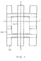
- FIG. 1 is a plan view
- FIG. 2 is a sectional view taken along the line X-X' in FIG. 1
- FIG. 3 is a sectional view taken along the line Y-Y' in FIG. 1.
- upper structures such as a shielding film 17 are omitted.
- Light-receiving portions 12, which are photodiodes, are formed in a semiconductor substrate 11. These light-receiving portions 12 are arranged in the substrate surface in a two-dimensional manner so that columnar arrays of a plurality of the light-receiving portions and CCD portions, which are not shown in the drawing, are placed alternately.
- comb-shaped transfer electrodes 14a and 14b as shown in FIG. 1 are formed via an insulating layer 13 so as not to cover the light-receiving portions 12, and an interlayer insulating film 16 further is formed.
- the metal shielding film 17 is formed thereon.
- this metal shielding film is provided with an opening in the portion above the light-receiving portions.
- a surface protection film 18 is formed thereon.
- an anti-reflection film 15 is formed between the light-receiving portions and the interlayer insulating film in the region where the light-receiving portions 12 are formed. This anti-reflection film considerably reduces the incident light reflection that has occurred on the substrate surface, thus improving the sensitivity behavior.
- the anti-reflection film 15 is formed of metal oxide that has a sufficient hydrogen permeability and a refractive index of at least 1.9, for example, at least 1.9 and not larger than 2.7.
- the metal oxide can be, for example, titanium oxide (refractive index of 2.2 to 2.7; the refractive index will be put in parentheses in the following), zirconium oxide (2.0 to 2.1), tantalum oxide (1.9 to 2.2), indium oxide (1.9 to 2.1) or niobium oxide (2.1 to 2.3). Since oxide films thereof have an excellent hydrogen permeability, the above-described dark current can be reduced effectively. In addition, since these oxide films have a smaller internal stress than a silicon nitride film, it is possible to reduce white marks that appear in an output image.
- a titanium oxide film (refractive index of 2.2 to 2.7) has a sufficiently higher refractive index than silicon nitride film (refractive index of 2.0), thus achieving anti-reflection effects more reliably.
- the titanium oxide has a higher refractive index in a short-wavelength range (for example, 400 nm) in a visible light region than in a long-wavelength range (for example, 700 nm).
- the refractive index of silicon has a similar distribution in the visible light region. Therefore, the use of the titanium oxide as the anti-reflection film can obtain an excellent anti-reflection effect in a wider wavelength range.
- This anti-reflection film 15 may have a multilayer structure of a plurality of above-mentioned oxide films laminated. Also, as described above, it is preferable that the anti-reflection film is formed after the electrode, so as to prevent the material of the anti-reflection film from serving as a pollution source for the electrode.
- a preferable form of a multilayer interference film that is formed above the light-receiving portions includes the silicon oxide film with a thickness of 50 nm or smaller, the anti-reflection film with a thickness of at least 10 nm and not larger than 70 nm, the interlayer insulating film with a thickness of at least 30 nm and not larger than 600 nm, and the surface protection film with a thickness of at least 100 nm and not larger than 300 nm in this order from the side of the light-receiving portions.
- the interlayer insulating film is not specifically limited and, for example, can be silicon oxide film.
- the interlayer insulating film is formed of a material having a lower refractive index than the anti-reflection film and the surface protection film.
- the surface protection film silicon nitride film, oxide films having a refractive index of at least 1.9 (for example, the various metal oxides preferable for the anti-reflection film as indicated above) or the like can be used.
- the anti-reflection film is formed so as to cover the region completely where the light-receiving portions are formed and at least a part of the region where the electrodes are formed.
- the anti-reflection film is formed so as to cover the region completely where the light-receiving portions are formed and at least a part of the region where the electrodes are formed.
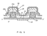
- FIGs. 4 to 6 show an example of the solid-state imaging device of the present invention that has the anti-reflection film formed to have such a preferable shape.
- FIG. 4 is a plan view
- FIG. 5 is a sectional view taken along the line X-X' in FIG. 4
- FIG. 6 is a sectional view taken along the line Y-Y' in FIG. 4.
- a shielding film 27 etc. is not shown in the drawings for simplicity.
- This preferable example is the same as the above-described embodiment (FIGs. 1 to 3) except for the shape of the anti-reflection film.
- a semiconductor substrate 21 in which light-receiving portions 22 are formed, an insulating film 23, transfer electrodes 24a and 24b, an anti-reflection film 25, an interlayer insulating film 26, a shielding film 27 and a surface protection film 28 are laminated.
- the material for forming the anti-reflection film 25 also is the same as that described above.
- the anti-reflection film that has been grown by a conventional method is used without pattern formation.
- the anti-reflection film is formed on the substrate plane including the region where the electrodes and the light-receiving portions are formed, as shown in FIG. 4.
- a solid-state imaging device described below has a structure similar to those shown in FIGs. 4 to 6 used for the description above.
- N-type impurities such as phosphorus were ion-implanted in a p-type silicon substrate 21, thereby forming photodiodes 22.
- an insulating film 23 formed of silicon oxide film with a thickness of 30 nm was grown by thermal oxidation.
- a polysilicon film with a thickness of 300 nm was grown by CVD (chemical vapor deposition), so as to form electrodes 24a and 24b by dry etching.
- An insulating film 29 formed of silicon nitride film had been formed between these polysilicon electrodes 24a, 24b and the insulating film 23 formed of silicon oxide film.
- an anti-reflection film 25 formed of titanium oxide film with a thickness of 20 nm was grown on an entire surface of the substrate by low pressure CVD.
- a silicon oxide film was grown by low pressure CVD so as to form an interlayer insulating film 26 with a thickness of 90 nm, then a shielding film 27 with a thickness of 400 nm formed of aluminum was formed by sputtering, followed by dry etching to provide an opening in the shielding film 27 above the photodiodes 22.
- the entire substrate surface was coated with a surface protection film 28 formed of silicon nitride film with a thickness of 120 nm by plasma CVD. Subsequently, heat-treatment under a hydrogen atmosphere at 450°C was performed for 30 minutes so as to obtain a solid-state imaging device.
- FIG. 7 shows the result of measuring the reflectance in a solid-state imaging device produced similarly to the present example except that silicon nitride film was used as the anti-reflection film.
- a solid-state imaging device was obtained in a similar manner to the first example except that films above photodiodes had a structure as in the following table.
- Film structure material
- Refractive index Film thickness nm
- Surface protective film silicon nitride film
- 2.0 111
- Layer insulating film silicon oxide film
- Anti-reflection film tantalum oxide film
- a solid-state imaging device was produced similarly to the above except that the anti-reflection film in the above table was changed to niobium oxide film (refractive index of 2.1) having a thickness equal to that of tantalum oxide film. The measurement of the spectral reflectance thereof achieved the same result as in FIG. 9. Moreover, a solid-state imaging device was produced similarly to the above except that the anti-reflection film in the above table was changed to titanium oxide film (refractive index of 2.3) having a thickness of 35 nm. The spectral reflectance thereof is shown in FIG. 10.
- the present invention is not limited to the above examples.
- the anti-reflection film formed of oxide with a refractive index of at least 1.9 is used, thereby supplying hydrogen to the substrate sufficiently so as to reduce the dark current. Also, since the anti-reflection film has a small internal stress, it is possible to reduce the white mark defects caused by the concentrated stress. Furthermore, because there is no limitation in a shape of the anti-reflection film, it becomes possible to form the anti-reflection film on the entire surface of the substrate, thereby achieving a simpler manufacturing process and still higher sensitivity. In addition, it also is possible to obtain the anti-reflection effect that is at least equal to or larger than the conventional one. Accordingly, the present invention can improve characteristics of a solid-state imaging device.
Landscapes
- Solid State Image Pick-Up Elements (AREA)
- Light Receiving Elements (AREA)
Applications Claiming Priority (1)
| Application Number | Priority Date | Filing Date | Title |
|---|---|---|---|
| PCT/JP1999/003601 WO2001003192A1 (en) | 1998-08-05 | 1999-07-02 | Solid state image sensing device and production method thereof |
Publications (1)
| Publication Number | Publication Date |
|---|---|
| EP1120832A1 true EP1120832A1 (de) | 2001-08-01 |
Family
ID=14236162
Family Applications (1)
| Application Number | Title | Priority Date | Filing Date |
|---|---|---|---|
| EP99926920A Withdrawn EP1120832A1 (de) | 1999-07-02 | 1999-07-02 | Festkörper -bildaufnahmevovrichtung und herstellungsverfahren |
Country Status (2)
| Country | Link |
|---|---|
| EP (1) | EP1120832A1 (de) |
| WO (1) | WO2001003192A1 (de) |
Family Cites Families (4)
| Publication number | Priority date | Publication date | Assignee | Title |
|---|---|---|---|---|
| JPH04152556A (ja) * | 1990-10-16 | 1992-05-26 | Canon Inc | 光半導体装置 |
| JPH08148665A (ja) * | 1994-11-22 | 1996-06-07 | Nec Corp | 固体撮像素子 |
| JPH11154741A (ja) * | 1997-11-20 | 1999-06-08 | Matsushita Electron Corp | 固体撮像素子およびその製造方法 |
| JPH10294446A (ja) * | 1998-03-13 | 1998-11-04 | Nec Corp | 固体撮像素子 |
-
1999
- 1999-07-02 EP EP99926920A patent/EP1120832A1/de not_active Withdrawn
- 1999-07-02 WO PCT/JP1999/003601 patent/WO2001003192A1/ja not_active Ceased
Non-Patent Citations (1)
| Title |
|---|
| See references of WO0103192A1 * |
Also Published As
| Publication number | Publication date |
|---|---|
| WO2001003192A1 (en) | 2001-01-11 |
Similar Documents
| Publication | Publication Date | Title |
|---|---|---|
| US8492804B2 (en) | Solid-state imaging device, method for producing same, and camera | |
| US8390707B2 (en) | Solid-state imaging device and manufacturing method thereof | |
| TWI442559B (zh) | 固態成像元件及其製造方法,固態成像裝置及成像裝置 | |
| KR20050045887A (ko) | 고체 촬상 장치 및 그 제조 방법 | |
| KR102721025B1 (ko) | 이미지 센서 및 이의 제조 방법 | |
| US7208811B2 (en) | Photo-detecting device | |
| CN102208425A (zh) | 固体摄像装置、固体摄像装置的制造方法和电子设备 | |
| US8507311B2 (en) | Method for forming an image sensing device | |
| JP3680512B2 (ja) | 固体撮像素子 | |
| TWI452682B (zh) | 光電轉換裝置 | |
| EP1120832A1 (de) | Festkörper -bildaufnahmevovrichtung und herstellungsverfahren | |
| JPH11214664A (ja) | 固体撮像素子およびその製造方法 | |
| JP2005033110A (ja) | 固体撮像素子及びその製造方法 | |
| JPH11154741A (ja) | 固体撮像素子およびその製造方法 | |
| JP4449298B2 (ja) | 固体撮像素子の製造方法および固体撮像素子 | |
| JPH04212459A (ja) | 固体撮像素子 | |
| JPH10326885A (ja) | 固体撮像素子 | |
| JPH0730090A (ja) | 固体撮像素子 | |
| JP4333615B2 (ja) | 固体撮像素子 | |
| JPH0338063A (ja) | カラー固体撮像素子及びその製造方法 | |
| TW437111B (en) | Structure and fabrication method of photodiode | |
| JPH03190272A (ja) | 固体撮像装置 | |
| JPS6046674A (ja) | 固体撮像装置 | |
| JP3733891B2 (ja) | 固体撮像素子及び固体撮像素子の製造方法 | |
| JPH0997890A (ja) | 固体撮像素子及びその製造方法 |
Legal Events
| Date | Code | Title | Description |
|---|---|---|---|
| PUAI | Public reference made under article 153(3) epc to a published international application that has entered the european phase |
Free format text: ORIGINAL CODE: 0009012 |
|
| 17P | Request for examination filed |
Effective date: 20010223 |
|
| AK | Designated contracting states |
Kind code of ref document: A1 Designated state(s): AT BE CH CY DE DK ES FI FR GB GR IE IT LI LU MC NL PT SE |
|
| RBV | Designated contracting states (corrected) |
Designated state(s): DE FR GB IT |
|
| STAA | Information on the status of an ep patent application or granted ep patent |
Free format text: STATUS: THE APPLICATION HAS BEEN WITHDRAWN |
|
| 18W | Application withdrawn |
Effective date: 20050415 |