EP1121759B1 - Seriell-parallel- und parallel-seriell-umwandlungsvorrichtung - Google Patents
Seriell-parallel- und parallel-seriell-umwandlungsvorrichtung Download PDFInfo
- Publication number
- EP1121759B1 EP1121759B1 EP99971163A EP99971163A EP1121759B1 EP 1121759 B1 EP1121759 B1 EP 1121759B1 EP 99971163 A EP99971163 A EP 99971163A EP 99971163 A EP99971163 A EP 99971163A EP 1121759 B1 EP1121759 B1 EP 1121759B1
- Authority
- EP
- European Patent Office
- Prior art keywords
- parallel
- memory
- data
- output
- serial
- Prior art date
- Legal status (The legal status is an assumption and is not a legal conclusion. Google has not performed a legal analysis and makes no representation as to the accuracy of the status listed.)
- Expired - Lifetime
Links
- 238000006243 chemical reaction Methods 0.000 title claims description 29
- 238000013507 mapping Methods 0.000 claims description 87
- 230000009977 dual effect Effects 0.000 claims description 32
- 238000000034 method Methods 0.000 claims description 12
- 238000005192 partition Methods 0.000 claims description 6
- 238000000638 solvent extraction Methods 0.000 claims description 3
- 238000004891 communication Methods 0.000 claims description 2
- 239000000872 buffer Substances 0.000 description 5
- 238000010586 diagram Methods 0.000 description 4
- 230000001419 dependent effect Effects 0.000 description 1
- 235000019800 disodium phosphate Nutrition 0.000 description 1
- 230000006870 function Effects 0.000 description 1
- 230000010363 phase shift Effects 0.000 description 1
- 238000012545 processing Methods 0.000 description 1
- 239000004065 semiconductor Substances 0.000 description 1
- 230000001360 synchronised effect Effects 0.000 description 1
- 238000012546 transfer Methods 0.000 description 1
Images





Classifications
-
- G—PHYSICS
- G11—INFORMATION STORAGE
- G11C—STATIC STORES
- G11C7/00—Arrangements for writing information into, or reading information out from, a digital store
- G11C7/10—Input/output [I/O] data interface arrangements, e.g. I/O data control circuits, I/O data buffers
- G11C7/1006—Data managing, e.g. manipulating data before writing or reading out, data bus switches or control circuits therefor
-
- H—ELECTRICITY
- H03—ELECTRONIC CIRCUITRY
- H03M—CODING; DECODING; CODE CONVERSION IN GENERAL
- H03M9/00—Parallel/series conversion or vice versa
-
- G—PHYSICS
- G11—INFORMATION STORAGE
- G11C—STATIC STORES
- G11C2207/00—Indexing scheme relating to arrangements for writing information into, or reading information out from, a digital store
- G11C2207/10—Aspects relating to interfaces of memory device to external buses
- G11C2207/107—Serial-parallel conversion of data or prefetch
Definitions
- the present invention relates to apparatus and method for converting serial bit streams into parallel bit streams and visa versa.
- digital data In many electronic systems, digital data must be transferred over a digital bus at a fixed rate (i.e., isochronous) between devices. These digital buses include a clock, synchronization signal and the data. The clock rate is fixed and both the synchronization signal and data are measured relative to it.
- a serial TDM bus the data is transferred one bit at a time (either MSB or LSB first) and the synchronization signal is used to mark the start of the data word.
- a parallel TDM bus all of the bits of the data are transferred at the same time. In the latter case, the synchronization signal is superfluous.
- Time Division Multiplexing is a known technique for combining N isochronous streams of digital data operating at the same frequency into one isochronous stream of data that operates at a new frequency M equal to N times the original frequency.
- the synchronization pulses still occur at the original frequency.
- the combined data transferred between synchronization pulses is called a frame.
- Each frame is broken into N equally sized pieces called time-slots.
- Each of the original streams are allotted one of the N time-slots per frame to transfer data.
- Each stream uses the same time-slot during each frame.
- the ST-Bus ⁇ defined by Mitel Semiconductor ⁇ uses a clock rate of 2.048 Mbits/second, 4.096 Mbits/second, or 8.192 Mbits/second with a frame rate of 8 kHz to combine 32, 64, or 128 64-Kbits/second serial streams into one stream.
- serial TDM buses have been used in favor of parallel TDM buses because serial TDM buses require fewer connections between devices.
- serial TDM buses require fewer connections between devices.
- multiple serial TDM streams running in parallel to achieve increased bandwidth (e.g., MVIP, SCSA, and H.110 computer telephony buses). These multiple streams are often referred to as a TDM highway.
- the data on the streams is to be processed by a computer, again the data must be converted from serial to parallel form. Often a single stream serial-to-parallel converter is incorporated into the computer. The serial port is connected to a switching device and other streams are then connected to the TDM highway.
- TDM highway data taken from the TDM highway is converted to parallel and stored in a memory device (e.g., a RAM) for use by the processor.
- the processor also places data to be transmitted on the TDM highway into the memory device, and the circuit converts this data from parallel to serial.
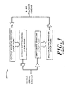
- FIG. 1 illustrates a block diagram of a prior art parallel-to-serial/serial-to-parallel conversion engine 18 for connecting to a serial stream. Each timeslot may be either driven from this circuit or received from a different circuit.
- the (tri-state) buffers illustrate that the same wires are used for input and output. The mechanism by which data is moved from the parallel stream into (and out of) the holding register as well as the control circuit for the tri-state buffers is not covered in this document.
- the shift registers are clocked at the bit rate of the serial stream (e.g., 8.192 MHz), however there is usually a phase shift of either 180° or 270° between the outgoing and incoming clocks.
- the outgoing data is moved from the output holding register to the output shift register.
- the incoming data is moved from the input shift register to the input holding register.
- the data in the shift registers is corrupted after only one bit-slot without the use of the holding registers. This is generally not enough time to move the data from multiple serial streams onto the parallel bus.
- U.S. Patent 5,463,630 also discloses the use of shift registers (SRI, SR2, u, SRn) to perform the conversions.
- apparatus for converting a serially received data word to a parallel output data word, said apparatus comprising: a serial data input interface that receives the serially received data word, and provides a received data word; a serial-to-parallel mapping circuit that receives said received data word and generates memory write control signals and memory write address signals; a memory device having a first port responsive to said memory write control signals and said memory write address signals for writing said received data word into said memory device, and a second port responsive to memory read control signals and memory read address signals for reading output data from said memory device; said serial-to-parallel mapping circuit comprises means for partitioning said received data word into a plurality of partitioned received data words and for generating said memory write control signals such that said partitioned received data words are written into said memory device at uniquely associated memory addresses; output interface circuitry that generates said memory read control signals and read address signals, and receives said output data from said memory device and reorders the bits of said output data to provide a parallel
- apparatus for converting a parallel received data word to a serially converted output data word
- said apparatus comprising: a parallel-to-serial input mapping circuit that receives the parallel received data word that includes a plurality of bits, and generates memory write control signals and memory write address signals, and also reorders said received parallel data word to provide a reordered parallel data word; a memory device having (i) a first port responsive to said memory write control signals and said write address signals for writing said reordered parallel data word into said memory device, and (ii) a second port responsive to memory read control signals and read address signals for reading data from said memory device; a parallel-to-serial output mapping circuit that generates said memory read control signals and said read address signals, and receives output data from said memory device and partitions said received output data into a plurality of serial data words; characterized in that said parallel-to-serial input mapping circuit reorders the bits of the parallel received data word written to said memory
- a method for conducting parallel data to serial data conversion comprising: receiving a parallel data word; reordering the bits of said received parallel data word to provide a reordered parallel data word; writing said reordered parallel data word to a memory device; reading output data from said memory device; partitioning said read output data into a plurality of serial data words; and providing a serially converted output data word from said plurality of partitioned serial data words.
- Reordering uses mapping interconnects as outlined above.
- a serial-to-parallel and parallel-to-serial converter comprising: a serial data input interface for receiving a serial input data word; an input memory connected to said serial data input interface and responsive to said receiving to convert said serial input data word into a parallel output data word, said input memory including a first memory device having a two memory banks; serial communication lines coupled to said input memory and operative to output said parallel output data word onto a parallel data bus; an output memory operative to receive a parallel input data word from said parallel data bus and to convert said received parallel input data word into a plurality of serial data words, said output memory including a second memory device; and a serial data output interface for receiving said plurality of serial data words and for providing a serially converted output data word.
- An output mapping circuit having connection mapping interconnects to the parallel output interface is also provided.
- the conversion engines of the present invention provide a bi-directional interface between a serial TDM highway and a parallel TDM highway.
- the present invention uses significantly fewer transistors and consumes significantly less power than earlier implementation.
- the amount of the savings increases as the number of streams in the serial TDM highway increases.
- CT computer telephony
- H.110 standard telephony bus
- the conversion engine of the present invention may be used in virtually any system that requires serial-to-parallel and/or parallel-to-serial data conversion.
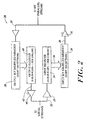
- FIG. 2 is a block diagram illustration of a serial-to-parallel/parallel-to-serial conversion engine 20 according to the present invention.
- the conversion engine may be located within a field programmable gate array (FPGA).
- the conversion engine 20 receives a plurality of serial data lines 22 (e.g., thirty-two) that are input to a serial input interface 24 via buffers 25. Each data line provides 128 time-slots operating at a bit rate of 8.192 MHz. Therefore, the thirty-two data lines (also known as "streams") provide a total of 4,096 time-slots.
- the serial input interface is preferably simply a plurality of clocked registers for capturing data from the serial data lines 22.
- the serial input interface 24 provides clocked data on lines 26 to an input bit shuffled memory device 28 that stores the data, and provides parallel output data on lines 30 to tri-state buffers 32 that output the data onto the thirty-two bit parallel bus 33.
- the details of how the input bit shuffled memory device 28 stores the data shall be discussed in detail hereinafter.
- the conversion engine 20 also receives parallel data from the thirty-two bit parallel bus 33, and stores the data in a output bit shuffled memory device 38.
- Data read from the memory device 38 is output to a serial data output interface 40 that provides a plurality of serial data output lines 42 (e.g., thirty-two) to a tri-state buffer 44 and onto the serial data lines 22.
- serial data output interface 40 that provides a plurality of serial data output lines 42 (e.g., thirty-two) to a tri-state buffer 44 and onto the serial data lines 22.
- FIG. 3 is a functional illustration of the serial-to-parallel conversion path of the conversion engine 20 illustrated in FIG. 2.
- the serial input interface 24 includes a plurality of clocked registers that provide clocked data on the lines 26 to a serial-to-parallel mapping circuit 44.
- the mapping circuit 44 partitions data received on the lines 26 into a plurality of segments. For example, in a preferred embodiment the clocked data is thirty-two bits wide and the serial-to-parallel mapping circuit 44 partitions the data into eight individual nibbles (i.e., four bits).
- the serial-to-parallel mapping circuit 44 then generates the necessary command (e.g., writes enables) and address signals to consecutively write the nibbles to a dual port memory device 46 (e.g., a RAM). Each of the nibbles is written to its own memory location within the dual port memory device 46.
- a dual port memory device 46 e.g., a RAM
- FIG. 5 is a pictorial illustration of labeled memory locations within the serial-to- parallel dual port memory 46 illustrated in FIG. 3.
- the memory device 46 includes two banks 48, 50 of memory, which allows information to be written to a first bank 48 at the same time that information is being read from a second bank 50.
- each bank 48,50 includes sixty-four separately write addressable four-bit memory locations.
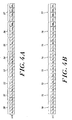
- the serial-to-parallel mapping circuit 44 partitions the thirty-two bit data word (FIG. 4A), for example into eight nibbles 50-57 (FIG. 4A).
- the eight nibbles 50-57 are then consecutively written to the memory device 46.
- the eight nibbles 50-57 are written into the first column of the first memory bank 48, which includes eight individually write addressable four-bit memory locations 60-67.
- nibble #1 50 (FIG. 4A) is written to memory location 0 60 (FIG. 5); nibble #2 51 (FIG.
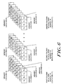
- FIG. 6 is another pictorial illustration of the layout of data within the dual port memory device 46 (FIG. 3). As shown, nibble #1 containing bits A 0 B 0 C 0 D 0 has been written to memory location 0, nibble #2 containing E 0 F 0 G 0 H 0 has been written to memory location 8, etc.
- the serial-to-parallel mapping circuit 44 (FIG. 3) clocks in the next thirty-two bits of data on the lines 26, and the thirty-two bits are partitioned into eight nibbles 70-77 (FIG. 4B).
- the eight nibbles 70-77 (FIG. 4B) are then consecutively written to the second column of the memory device 46 (FIG. 5), which includes eight individually write addressable four-bit memory locations. Specifically, nibble #170 (FIG. 4B) is written to memory location 1 80 (FIG. 5); nibble #2 71 (FIG. 4B), is written to memory location 9 81 (FIG. 5); nibble #3 72 (FIG.
- nibble #1 containing bits A 1 B 1 C 1 D 1 has been written to memory location 1 and nibble #2 containing E 1 F 1 G 1 H 1 has been written to memory location 9.
- the nibbles #3-#7 are written to their associated memory location, and nibble #8 containing CC 1 DD 1 EE 1 FF 1 is written to memory location 57.
- the next series of writes occur in the second bank 50 and reads in the first bank 48.
- the dual port memory device 46 may include eight 16x4 bit dual ports RAMs that collectively define the memory device 46, wherein each of the RAMs provides one the eight columns illustrated in FIGs. 5 and 6.
- the dual port memory device may include a single 16x32 bit dual port RAM.
- the second bank 50 (FIG. 5) is being read by a parallel output mapping circuit 92 (FIG. 3).
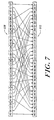
- FIG. 7 illustrates bit mapping ("shuffling") between the output mapping circuit 92 (FIG. 3) and parallel output interface 109 (FIG. 3) to provide an output formatted for use by processing devices (e.g., DSPs).
- thirty-two bit word 110 represents the contents of the output mapping circuit 92 (FIG. 3)
- thirty-two bit word 112 represents the contents of the parallel output interface 109 (FIG. 3).
- words 110 and 112 include the same bits, but some of the bit positions have been changed. This change is performed by mapping the interconnects between the output mapping circuit 92 and the parallel output interface 109.
- bit A 1 is located in the fifth bit position of the word 110 located in the output mapping circuit 92 (FIG.
- the interconnects between the output mapping circuit 92 and the parallel output interface 109 are configured such that the bit A 1 is mapped into the second bit position of the word 112 located in the parallel output interface 109 (FIG. 3).
- Bit B 0 is located in the second bit position of the output mapping circuit 92 and when it is clocked into the parallel output interface 109 it is placed in the ninth bit position due to the interconnect mapping.
- the remaining mappings are shown in FIG. 7.
- the parallel output interface preferably includes a thirty-two bit clocked register.
- the serial-to-parallel/parallel-to-serial conversion engine 20 also includes a parallel-to-serial conversion path comprising the output bit shuffled memory device 38 and the serial data output interface 40.
- FIG. 8 is a functional illustration to the parallel-to-serial conversion path.
- the output bit shuffled memory device 38 includes a parallel-to-serial input mapping circuit 130 that comprises a plurality of clocked registers.
- the clocked data is thirty-two bits wide and therefore the mapping circuit 130 includes thirty-two registers.
- the parallel-to-serial mapping circuit 130 also generates command signals (e.g., writes enables) and address signals for writing the data in the circuit 130 into a parallel-to-serial dual port memory 132.
- command signals e.g., writes enables
- address signals for writing the data in the circuit 130 into a parallel-to-serial dual port memory 132.
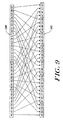
- FIG. 9 is a pictorial illustration of the bit mapping between the parallel-to-serial mapping circuit 130 (FIG. 8) and the dual port memory 132 (FIG. 8).
- thirty-two bit word 140 represents the data received by the parallel-to-seriat input mapping circuit 130 (FIG. 8)
- thirty-two bit word 142 represents the data received by the parallel-to-serial dual port memory 132.
- the words 140 and 142 include the same bits, but some of the bit positions have been changed.
- the position changes are performed by mapping of the interconnects between the parallel-to-serial input mapping circuit 130 and the parallel-to-serial dual port memory 132, as shown in FIG. 9.
- the entire word 142 is written into the parallel-to-serial dual port memory 132.
- FIG. 10 is a pictorial illustration of labeled memory locations within the parallel-to-serial dual port memory 132 illustrated in FIG. 8.
- the memory device 132 also includes two banks 147, 148.
- the data word 142 is written into write address 0 150 as shown in FIG. 10.
- the next data word is written to write location 1 152.
- Subsequent writes continue up column 154 until the eighth word is written to write address location 7 156.
- the next write occurs in the second bank 148 of the memory device and occurs at write location 8 160 , and writes continue up the column 154.
- the next write wraps around to memory location 0 150 and the writes continue up the column 154 again.
- the parallel-to-serial conversion path also includes a parallel-to-serial output mapping circuit 164 that reads data from the dual port memory device 132.
- the parallel-to-serial output mapping circuit 164 generates the address signals and control signals to read data from the memory device 132.
- the input mapping circuit 130 is writing data to the first bank 147 (FIG. 10) of the dual port memory device 132
- the output mapping circuit 164 is reading data from second bank 148 (FIG. 10).
- the read accesses start at read addresses 0 166 and continues up the column with addresses 8, 16, 24, 32, 40, 48 and 56 (FIG. 10). Each of these read addresses contains four-bits of data.
- each read provides a nibble of data that is placed in the parallel-to-serial output mapping circuit 164.
- FIG. 11 illustrates a data word 180 resident in the output mapping circuit 164.
- the conversion engine switches reads and writes back and forth between the first and second banks of the memory devices.
- the present invention may be used with systems where the bit rates of the serial streams are not equal. However, the ratio of the larger frequency to the smaller frequency should be a factor of two. In this case the parallel bus is operated at the higher of the frequencies and the rate at which each bit of the input and output registers is adjusted to the proper rate. In this embodiment the data from any "extra" memory reads is ignored.
- the present invention has been discussed in the context of eight bit words and certain clock rates and memory sizes, one of ordinary skill in the art will recognize that the present invention is not so limited. It is contemplated that the present invention shall be employed in system that use different word sizes, and the sizes of the corresponding circuitry will changed accordingly to provide an efficient serial-to-parallel and/or a parallel-to-serial conversion engine. In addition, the present invention is certainly not limited to interfacing with a 32-bit TDM highway. Furthermore, although the present invention presented a preferred embodiment that employs dual port memory devices, it is contemplated that in an alternative embodiment single port memory devices may be combined and the necessary control logic added to perform the function of the dual port memory devices set forth herein.
- bit shuffling decoder logic may be located between the memory device 46 and the output mapping circuit 92 to perform the bit "shuffling", thus eliminating the mapping (i.e., crisscrossing) of the interconnects between the output mapping circuit and the parallel output interface.
Landscapes
- Engineering & Computer Science (AREA)
- Theoretical Computer Science (AREA)
- Time-Division Multiplex Systems (AREA)
- Static Random-Access Memory (AREA)
- Dram (AREA)
Claims (12)
- Vorrichtung, die dazu ausgelegt ist, ein seriell empfangenes Datenwort in ein paralleles Ausgangsdatenwort umzuwandeln, wobei die Vorrichtung. (24, 28) umfasst:wobei die Abbildungsschaltung (44) ein Mittel umfasst, das dazu ausgelegt ist, das empfangene Datenwort in eine Vielzahl von unterteilten empfangenen Datenworten (50, 51, 52, 53, 54, 55, 56, 57) zu unterteilen und die Speicherschreib-Steuersignale derart zu erzeugen, dass die unterteilten empfangenen Datenworte (50, 51, 52, 53, 54, 55, 56, 57) in das Speicherbauelement (46) an eindeutig zugeordneten Speicheradressen (48, 50, 80, 81, 82, 84) geschrieben werden;eine serielle Dateneingangsschnittstelle (24), die dazu ausgelegt ist, das seriell empfangene Datenwort zu empfangen und ein empfangenes Datenwort zu liefern;eine Abbildungsschaltung (44), die dazu ausgelegt ist, das empfangene Datenwort zu empfangen und Speicherschreib-Steuersignale und Speicherschreib-Adressensignale zu erzeugen;ein Speicherbauelement (46) mit einem ersten Anschluss, der dazu ausgelegt ist, auf die Speicherschreib-Steuersignale und die Speicherschreib-Adressensignale zum Schreiben des empfangenen Datenworts in das Speicherbauelement (46) zu reagieren, und einem zweiten Anschluss, der dazu ausgelegt ist, auf Speicherlese-Steuersignale und Speicherlese-Adressensignale zum Lesen von Ausgangsdaten aus dem Speicherbauelement (46) zu reagieren;
eine Ausgangsschnittstellenschaltung (92, 109), die dazu ausgelegt ist, die Speicherlese-Steuersignale und -lese-Adressensignale zu erzeugen, und dazu ausgelegt ist, die Ausgangsdaten (94) vom Speicherbauelement (46) zu empfangen und die Bits der Ausgangsdaten (94) umzuordnen, um ein paralleles Ausgangsdatenwort (110) zu liefern,
dadurch gekennzeichnet, dass
die Ausgangsschnittstellenschaltung (92, 109) eine Ausgangsabbildungsschaltung (92), die auf die Ausgangsdaten (110) reagiert, und eine parallele Ausgangsschnittstelle (109) umfasst, wobei die Umordnung der Bits des Ausgangsdatenworts (110) durch Abbilden von Zwischenverbindungen zwischen einem Ausgangsanschluss der Ausgangsabbildungsschaltung (92) und einem Eingangsanschluss der parallelen Ausgangsschnittstelle (109) durchgeführt wird, wobei die parallele Ausgangsschnittstelle (109) auch einen parallelen Ausgangsschnittstellen-Ausgangsanschluss (30) umfasst, der dazu ausgelegt ist, das parallele Ausgangsdatenwort (112) zu liefern. - Vorrichtung nach Anspruch 1, wobei die Ausgangsschnittstellenschaltung (92, 109) eine Ausgangsabbildungsschaltung (92) umfasst, die dazu ausgelegt ist, ein Wort aus dem Speicherbauelement (46) zu lesen, wobei das aus dem Speicher (92) gelesene Wort eine gleiche Anzahl von Bits wie das seriell empfangene Datenwort aufweist.
- Vorrichtung nach Anspruch 1, wobei die serielle Dateneingangsschnittstelle (24) das seriell empfangene Datenwort mit einer ersten Rate eintaktet und die Abbildungsschaltung (44) Daten mit einer zweiten Rate mit einer Frequenz, die achtmal schneller ist als die erste Rate, taktet.
- Vorrichtung (38), die dazu ausgelegt ist, ein parallel empfangenes Datenwort in ein seriell umgewandeltes Ausgangsdatenwort umzuwandeln, wobei die Vorrichtung umfasst:dadurch gekennzeichnet, dasseine Eingangsabbildungsschaltung (130), die dazu ausgelegt ist, das parallele empfangene Datenwort, das eine Vielzahl von Bits umfasst, zu empfangen, und dazu ausgelegt ist, Speicherschreib-Steuersignale und Speicherschreib-Adressensignale zu erzeugen, und auch dazu ausgelegt ist, das empfangene parallele Datenwort umzuordnen, um ein umgeordnetes paralleles Datenwort zu liefern;ein Speicherbauelement (132) mit(i) einem ersten Anschluss, der dazu ausgelegt ist, auf die Speicherschreib-Steuersignale und die Schreib-Adressensignale zum Schreiben des umgeordneten parallelen Datenworts (142) in das Speicherbauelement (132) zu reagieren, und(ii) einem zweiten Anschluss, der dazu ausgelegt ist, auf Speicherlese-Steuersignale und -lese-Adressensignale zum Lesen von Daten aus dem Speicherbauelement zu reagieren;eine Ausgangsabbildungsschaltung (164), die dazu ausgelegt ist, die Speicherlese-Steuersignale und die Lese-Adressensignale zu erzeugen, und dazu ausgelegt ist, Ausgangsdaten vom Speicherbauelement (132) zu empfangen und die empfangenen Ausgangsdaten in eine Vielzahl von seriellen Datenworten zu unterteilen;
die Eingangsabbildungsschaltung (130) dazu ausgelegt ist, die Bits des parallelen empfangenen Datenworts, das in das Speicherbauelement geschrieben wird, durch Abbilden von Zwischenverbindungen zwischen der Eingangsabbildungsschaltung (130) und dem Speicherbauelement (132) umzuordnen, um das umgeordnete parallele Datenwort zu liefern, und dass die Vorrichtung auch eine serielle Datenausgangsschnittstelle 40 umfasst, die dazu ausgelegt ist, die Vielzahl von seriellen Datenworten zu empfangen und das seriell umgewandelte Ausgangsdatenwort zu liefern. - Vorrichtung nach Anspruch 4, wobei das Speicherbauelement (132) als Doppelzugriffs-Speicherbauelement ausgelegt ist, das zumindest eine erste Bank (147) von Speicherstellen und eine zweite Bank (148) von Speicherstellen umfasst, wobei, während Daten in die Speicherstellen (150, 152) der ersten Bank (147) unter der Steuerung der Eingangsabbildungsschaltung (130) geschrieben werden, Daten aus den Speicherstellen der zweiten Bank (148) unter der Steuerung der Ausgangsabbildungsschaltung (164) gelesen werden können.
- Verfahren zum Durchführen einer Umwandlung von parallelen Daten in serielle Daten, wobei das Verfahren umfasst:Empfangen eines parallelen Datenworts (140) an einer Eingangsabbildungsschaltung (130);Umordnen der Bits des empfangenen parallelen Datenworts (140), um ein umgeordnetes paralleles Datenwort (142) zu liefern;Schreiben des umgeordneten parallelen Datenworts in ein Speicherbauelement (132);Lesen von Ausgangsdaten aus dem Speicherbauelement (132);Unterteilen der gelesenen Ausgangsdaten in eine Vielzahl von seriellen Datenworten; undLiefern eines seriell umgewandelten Ausgangsdatenworts von der Vielzahl von unterteilten seriellen Datenworten; dadurch gekennzeichnet, dass der Schritt des Umordnens unter Verwendung von Abbildungszwischenverbindungen zwischen der Eingangsabbildungsschaltung (130) und dem Speicherbauelement (132) durchgeführt wird.
- Verfahren nach Anspruch 6, wobei das Schreiben umfasst:Schreiben des umgeordneten empfangenen parallelen Datenworts (142) in einen ersten Anschluss des Speicherbauelements (132).
- Verfahren nach Anspruch 6, wobei das Lesen umfasst:Lesen von Daten von einem zweiten Anschluss des Speicherbauelements (132).
- Serien-Parallel- und Parallel-Serien-Umsetzer (20) mit:gekennzeichnet durcheiner seriellen Dateneingangsschnittstelle (24), die dazu ausgelegt ist, ein serielles Eingangsdatenwort zu empfangen;einem Eingangsspeicher (28), der mit der seriellen Dateneingangsschnittstelle (24) verbunden ist und dazu ausgelegt ist, ein empfangenes serielles Eingangsdatenwort in ein paralleles Ausgangsdatenwort umzuwandeln, wobei der Eingangsspeicher (28) ein erstes Speicherbauelement (46) umfasst;einem Ausgangsspeicher (38), der wirksam ist, um ein paralleles Eingangsdatenwort von dem parallelen Datenbus (33) zu empfangen und das empfangene parallele Eingangsdatenwort in eine Vielzahl von seriellen Datenworten umzuwandeln, wobei der Ausgangsspeicher (38) ein zweites Speicherbauelement (132) umfasst; undeiner seriellen Datenausgangsschnittstelle (40), die dazu ausgelegt ist, die Vielzahl von seriellen Datenworten zu empfangen und ein seriell umgewandeltes Ausgangsdatenwort zu liefern;
eine Ausgangsabbildungsschaltung (92) in Verbindung mit dem ersten Speicherbauelement (46);
eine parallele Ausgangsschnittstelle (109); und
eine Verbindung zwischen der Ausgangsabbildungsschaltung (92) und der parallelen Ausgangsschnittstelle (109), wobei die Verbindung Zwischenverbindungen zwischen einem Ausgangsanschluss der Ausgangsabbildungsschaltung (92) und einem Eingangsanschluss der parallelen Ausgangsschnittstelle (109) abbildet. - Umsetzer (20) nach Anspruch 9, wobei der Eingangsspeicher (28) umfasst:eine Abbildungsschaltung (44), die auf das Empfangen reagiert, um Schreibsteuersignale und Schreibadressensignale zum ersten Speicherbauelement (46) zu liefern.
- Umsetzer (20) nach Anspruch 9, wobei die Verbindung, die die Zwischenverbindungen abbildet, wirksam ist, um die Bits eines Ausgangsdatenworts vom ersten Speicherbauelement (46) umzuordnen, um das parallele Ausgangsdatenwort zu liefern.
- Umsetzer nach Anspruch 9, wobei das zweite Speicherbauelement (132) zwei Speicherbänke (48, 50) für das zweite Speicherbauelement umfasst, wobei die zwei Speicherbänke das Schreiben von Daten in eine erste (48) der zwei Speicherbänke für das zweite Speicherbauelement zur gleichen Zeit wie das Lesen von Daten aus einer zweiten (50) der zwei Speicherbänke für das zweite Speicherbauelement ermöglichen.
Applications Claiming Priority (4)
| Application Number | Priority Date | Filing Date | Title |
|---|---|---|---|
| US10536998P | 1998-10-23 | 1998-10-23 | |
| US105369P | 1998-10-23 | ||
| US09/427,669 US6684275B1 (en) | 1998-10-23 | 1999-10-23 | Serial-to-parallel/parallel-to-serial conversion engine |
| PCT/US1999/024853 WO2000025431A1 (en) | 1998-10-23 | 1999-10-23 | Serial-to-parallel/parallel-to-serial conversion engine |
Publications (2)
| Publication Number | Publication Date |
|---|---|
| EP1121759A1 EP1121759A1 (de) | 2001-08-08 |
| EP1121759B1 true EP1121759B1 (de) | 2005-07-20 |
Family
ID=30117708
Family Applications (1)
| Application Number | Title | Priority Date | Filing Date |
|---|---|---|---|
| EP99971163A Expired - Lifetime EP1121759B1 (de) | 1998-10-23 | 1999-10-23 | Seriell-parallel- und parallel-seriell-umwandlungsvorrichtung |
Country Status (4)
| Country | Link |
|---|---|
| US (2) | US6684275B1 (de) |
| EP (1) | EP1121759B1 (de) |
| CA (1) | CA2347230C (de) |
| WO (1) | WO2000025431A1 (de) |
Families Citing this family (26)
| Publication number | Priority date | Publication date | Assignee | Title |
|---|---|---|---|---|
| US6820148B1 (en) | 2000-08-17 | 2004-11-16 | Sandisk Corporation | Multiple removable non-volatile memory cards serially communicating with a host |
| JP2002196846A (ja) * | 2000-12-26 | 2002-07-12 | Mitsubishi Electric Corp | Lsiのリーク電流低減方法 |
| US6854045B2 (en) * | 2001-06-29 | 2005-02-08 | Intel Corporation | Hardware emulation of parallel ATA drives with serial ATA interface |
| ITVA20010035A1 (it) * | 2001-10-16 | 2003-04-16 | St Microelectronics Srl | Dispositivo di memoria non volatile con doppia interfaccia di comunicazione seriale/parallela |
| US7996588B2 (en) * | 2002-10-04 | 2011-08-09 | Hewlett-Packard Company | Method and apparatus for real-time transport of multi-media information in a network |
| JP4257830B2 (ja) * | 2003-03-11 | 2009-04-22 | パナソニック株式会社 | データ送受信装置 |
| JP4594930B2 (ja) * | 2003-06-03 | 2010-12-08 | スターレント・ネットワークス・エルエルシー | データを再フォーマットするためのシステムおよび方法 |
| GB0405283D0 (en) * | 2004-03-09 | 2004-04-21 | Aspex Technology Ltd | Multi-port memory for flexible and space efficient corner turning networks in associative processors |
| US7084664B1 (en) * | 2004-06-14 | 2006-08-01 | Alter Corporation | Integrated circuits with reduced interconnect overhead |
| US7603514B2 (en) * | 2005-03-31 | 2009-10-13 | Intel Corporation | Method and apparatus for concurrent and independent data transfer on host controllers |
| US7298302B1 (en) * | 2006-05-17 | 2007-11-20 | Texas Instruments Incorporated | System and method for presenting serial drive signals for effecting communication of a plurality of parallel data signals |
| US20090161750A1 (en) * | 2007-12-19 | 2009-06-25 | Marc Racicot | Multiplexing video using a dsp |
| US9092582B2 (en) * | 2010-07-09 | 2015-07-28 | Cypress Semiconductor Corporation | Low power, low pin count interface for an RFID transponder |
| US9846664B2 (en) | 2010-07-09 | 2017-12-19 | Cypress Semiconductor Corporation | RFID interface and interrupt |
| TWI616756B (zh) * | 2013-07-30 | 2018-03-01 | National Taiwan University Of Science And Technology | 具非揮發性記憶體之串並列傳輸介面電路 |
| KR102251809B1 (ko) | 2014-05-28 | 2021-05-13 | 삼성전자주식회사 | 메모리 시스템, 메모리 인터페이스 장치 및 메모리 시스템에서의 인터페이싱 방법 |
| US11012087B2 (en) * | 2017-11-23 | 2021-05-18 | M31 Technology Corporation | Encoding and decoding architecture for high speed data communication system and related physical layer circuit, transmitter and receiver and communication system thereof |
| EP3959140B1 (de) * | 2019-04-25 | 2026-01-07 | AeroVironment, Inc. | Bodenunterstützungsausrüstung für ein flugzeug für hohe flughöhen und lange flugdauern. |
| WO2020226908A1 (en) | 2019-04-25 | 2020-11-12 | Aerovironment, Inc. | Method of managing a fleet of high altitude long endurance aircraft |
| SG11202111296TA (en) | 2019-04-25 | 2021-11-29 | Aerovironment Inc | Methods of climb and glide operations of a high altitude long endurance aircraft |
| AU2020262292B2 (en) * | 2019-04-25 | 2025-08-21 | Aerovironment, Inc. | Systems and methods for distributed control computing for a high altitude long endurance aircraft |
| US11518514B2 (en) | 2019-04-25 | 2022-12-06 | Aerovironment, Inc | Off-center parachute flight termination system including latch mechanism disconnectable by burn wire |
| AU2020315515B2 (en) | 2019-04-25 | 2025-12-04 | Aerovironment, Inc. | Method of operating a high altitude long endurance aircraft for maximizing solar capture |
| AU2020307360B2 (en) | 2019-04-25 | 2025-09-25 | Aerovironment, Inc. | Method of flight plan optimization of a high altitude long endurance aircraft |
| CN115461733A (zh) * | 2020-03-02 | 2022-12-09 | 微芯片技术股份有限公司 | 将多个串行通信接口与并行通信接口对接、以及相关系统、方法和装置 |
| TWI854675B (zh) * | 2023-05-30 | 2024-09-01 | 睿寬智能科技有限公司 | 重排ldpc碼而改善ldpc重組解碼器並行的方法 |
Family Cites Families (11)
| Publication number | Priority date | Publication date | Assignee | Title |
|---|---|---|---|---|
| US4924464A (en) | 1989-03-13 | 1990-05-08 | American Telephone And Telegraph Company | Technique for converting either way between a plurality of N synchronized serial bit streams and a parallel TDM format |
| DE4323521A1 (de) | 1993-07-14 | 1995-01-19 | Sel Alcatel Ag | Verfahren zum Umsetzen eines parallelisierten, zeitlich gemultiplexten Datenstroms in einzelne serielle Datenströme und umgekehrt, sowie Umsetzer dafür |
| JP3133601B2 (ja) * | 1994-02-09 | 2001-02-13 | 株式会社東芝 | パラレル・シリアル変換装置及びこれを用いた線形変換装置 |
| TW293107B (de) * | 1994-10-28 | 1996-12-11 | Matsushita Electric Industrial Co Ltd | |
| JP3233561B2 (ja) * | 1994-10-28 | 2001-11-26 | 松下電器産業株式会社 | 半導体記憶装置 |
| US5862367A (en) * | 1995-03-17 | 1999-01-19 | United Micro Electronics Corporation | Apparatus and method for serial-to-parallel data conversion and transmission |
| US5926120A (en) * | 1996-03-28 | 1999-07-20 | National Semiconductor Corporation | Multi-channel parallel to serial and serial to parallel conversion using a RAM array |
| US5812881A (en) * | 1997-04-10 | 1998-09-22 | International Business Machines Corporation | Handshake minimizing serial to parallel bus interface in a data processing system |
| JPH1153301A (ja) * | 1997-08-06 | 1999-02-26 | Kobe Nippon Denki Software Kk | バス・アービトレーション・インタフェース |
| US6128681A (en) * | 1997-08-07 | 2000-10-03 | Avid Technology, Inc. | Serial to parallel and parallel to serial, converter for a digital audio workstation |
| US6140946A (en) * | 1997-11-07 | 2000-10-31 | International Business Machines Corporation | Asynchronous serialization/deserialization system and method |
-
1999
- 1999-10-23 EP EP99971163A patent/EP1121759B1/de not_active Expired - Lifetime
- 1999-10-23 CA CA002347230A patent/CA2347230C/en not_active Expired - Fee Related
- 1999-10-23 US US09/427,669 patent/US6684275B1/en not_active Expired - Fee Related
- 1999-10-23 WO PCT/US1999/024853 patent/WO2000025431A1/en not_active Ceased
-
2003
- 2003-07-02 US US10/612,863 patent/US20040098517A1/en not_active Abandoned
Also Published As
| Publication number | Publication date |
|---|---|
| EP1121759A1 (de) | 2001-08-08 |
| WO2000025431A1 (en) | 2000-05-04 |
| US6684275B1 (en) | 2004-01-27 |
| CA2347230A1 (en) | 2000-05-04 |
| US20040098517A1 (en) | 2004-05-20 |
| CA2347230C (en) | 2005-12-20 |
Similar Documents
| Publication | Publication Date | Title |
|---|---|---|
| EP1121759B1 (de) | Seriell-parallel- und parallel-seriell-umwandlungsvorrichtung | |
| EP0666653B1 (de) | Ein-/Ausgabedatenports | |
| US5261064A (en) | Burst access memory | |
| US5440523A (en) | Multiple-port shared memory interface and associated method | |
| US6741193B2 (en) | Parallel in serial out circuit having flip-flop latching at multiple clock rates | |
| EP2629299A1 (de) | Speichersystem und Verfahren mit seriellem und parallelen Modi | |
| JPH01217575A (ja) | ビデオプロセッサシステム | |
| WO2008037064A1 (en) | Packet based id generation for serially interconnected devices | |
| US5602848A (en) | Multi-mode TDM interface circuit | |
| US4903240A (en) | Readout circuit and method for multiphase memory array | |
| US5596578A (en) | Time division multiplexing data transfer system for digital audio data distribution | |
| EP1384357B1 (de) | Architekturen für einen einstufigen schalter | |
| JPH03105789A (ja) | 半導体記憶装置 | |
| US5818834A (en) | Serial bit rate converter embedded in a switching matrix | |
| US5319596A (en) | Semiconductor memory device employing multi-port RAMs | |
| JPH09502579A6 (ja) | Tdmスイッチング・マトリックスのための直列ビット伝送速度変換器 | |
| EP0421627A2 (de) | Speichervorrichtung | |
| US7315540B2 (en) | Random access memory based space time switch architecture | |
| CN1856835A (zh) | 同步的ram存储电路 | |
| US6445394B1 (en) | Serialized mapped memory configuration for a video graphics chip | |
| JPH10214220A (ja) | 集積回路 | |
| JPH0445698A (ja) | 信号情報のチャンネル同期交換の方法 | |
| JPH01176197A (ja) | 時分割多元交換方式 | |
| JPS61193523A (ja) | 半導体論理集積装置 | |
| JPS5940797A (ja) | 時間スイツチ回路 |
Legal Events
| Date | Code | Title | Description |
|---|---|---|---|
| PUAI | Public reference made under article 153(3) epc to a published international application that has entered the european phase |
Free format text: ORIGINAL CODE: 0009012 |
|
| 17P | Request for examination filed |
Effective date: 20010420 |
|
| AK | Designated contracting states |
Kind code of ref document: A1 Designated state(s): AT BE CH CY DE DK ES FI FR GB GR IE IT LI LU MC NL PT SE |
|
| 17Q | First examination report despatched |
Effective date: 20010718 |
|
| RAP1 | Party data changed (applicant data changed or rights of an application transferred) |
Owner name: POLYCOM, INC. |
|
| GRAP | Despatch of communication of intention to grant a patent |
Free format text: ORIGINAL CODE: EPIDOSNIGR1 |
|
| GRAS | Grant fee paid |
Free format text: ORIGINAL CODE: EPIDOSNIGR3 |
|
| GRAA | (expected) grant |
Free format text: ORIGINAL CODE: 0009210 |
|
| RIN1 | Information on inventor provided before grant (corrected) |
Inventor name: GOLDSTEIN, JASON, A. |
|
| AK | Designated contracting states |
Kind code of ref document: B1 Designated state(s): AT BE CH CY DE DK ES FI FR GB GR IE IT LI LU MC NL PT SE |
|
| PG25 | Lapsed in a contracting state [announced via postgrant information from national office to epo] |
Ref country code: LI Free format text: LAPSE BECAUSE OF FAILURE TO SUBMIT A TRANSLATION OF THE DESCRIPTION OR TO PAY THE FEE WITHIN THE PRESCRIBED TIME-LIMIT Effective date: 20050720 Ref country code: IT Free format text: LAPSE BECAUSE OF FAILURE TO SUBMIT A TRANSLATION OF THE DESCRIPTION OR TO PAY THE FEE WITHIN THE PRESCRIBED TIME-LIMIT;WARNING: LAPSES OF ITALIAN PATENTS WITH EFFECTIVE DATE BEFORE 2007 MAY HAVE OCCURRED AT ANY TIME BEFORE 2007. THE CORRECT EFFECTIVE DATE MAY BE DIFFERENT FROM THE ONE RECORDED. Effective date: 20050720 Ref country code: FI Free format text: LAPSE BECAUSE OF FAILURE TO SUBMIT A TRANSLATION OF THE DESCRIPTION OR TO PAY THE FEE WITHIN THE PRESCRIBED TIME-LIMIT Effective date: 20050720 Ref country code: ES Free format text: LAPSE BECAUSE OF FAILURE TO SUBMIT A TRANSLATION OF THE DESCRIPTION OR TO PAY THE FEE WITHIN THE PRESCRIBED TIME-LIMIT Effective date: 20050720 Ref country code: CH Free format text: LAPSE BECAUSE OF FAILURE TO SUBMIT A TRANSLATION OF THE DESCRIPTION OR TO PAY THE FEE WITHIN THE PRESCRIBED TIME-LIMIT Effective date: 20050720 Ref country code: BE Free format text: LAPSE BECAUSE OF FAILURE TO SUBMIT A TRANSLATION OF THE DESCRIPTION OR TO PAY THE FEE WITHIN THE PRESCRIBED TIME-LIMIT Effective date: 20050720 Ref country code: AT Free format text: LAPSE BECAUSE OF FAILURE TO SUBMIT A TRANSLATION OF THE DESCRIPTION OR TO PAY THE FEE WITHIN THE PRESCRIBED TIME-LIMIT Effective date: 20050720 |
|
| REG | Reference to a national code |
Ref country code: GB Ref legal event code: FG4D |
|
| REG | Reference to a national code |
Ref country code: CH Ref legal event code: EP |
|
| REG | Reference to a national code |
Ref country code: IE Ref legal event code: FG4D |
|
| REF | Corresponds to: |
Ref document number: 69926252 Country of ref document: DE Date of ref document: 20050825 Kind code of ref document: P |
|
| PG25 | Lapsed in a contracting state [announced via postgrant information from national office to epo] |
Ref country code: SE Free format text: LAPSE BECAUSE OF FAILURE TO SUBMIT A TRANSLATION OF THE DESCRIPTION OR TO PAY THE FEE WITHIN THE PRESCRIBED TIME-LIMIT Effective date: 20051020 Ref country code: GR Free format text: LAPSE BECAUSE OF FAILURE TO SUBMIT A TRANSLATION OF THE DESCRIPTION OR TO PAY THE FEE WITHIN THE PRESCRIBED TIME-LIMIT Effective date: 20051020 Ref country code: DK Free format text: LAPSE BECAUSE OF FAILURE TO SUBMIT A TRANSLATION OF THE DESCRIPTION OR TO PAY THE FEE WITHIN THE PRESCRIBED TIME-LIMIT Effective date: 20051020 |
|
| PG25 | Lapsed in a contracting state [announced via postgrant information from national office to epo] |
Ref country code: CY Free format text: LAPSE BECAUSE OF FAILURE TO SUBMIT A TRANSLATION OF THE DESCRIPTION OR TO PAY THE FEE WITHIN THE PRESCRIBED TIME-LIMIT Effective date: 20051023 |
|
| PG25 | Lapsed in a contracting state [announced via postgrant information from national office to epo] |
Ref country code: IE Free format text: LAPSE BECAUSE OF NON-PAYMENT OF DUE FEES Effective date: 20051024 |
|
| PG25 | Lapsed in a contracting state [announced via postgrant information from national office to epo] |
Ref country code: MC Free format text: LAPSE BECAUSE OF NON-PAYMENT OF DUE FEES Effective date: 20051031 Ref country code: LU Free format text: LAPSE BECAUSE OF NON-PAYMENT OF DUE FEES Effective date: 20051031 |
|
| PG25 | Lapsed in a contracting state [announced via postgrant information from national office to epo] |
Ref country code: PT Free format text: LAPSE BECAUSE OF FAILURE TO SUBMIT A TRANSLATION OF THE DESCRIPTION OR TO PAY THE FEE WITHIN THE PRESCRIBED TIME-LIMIT Effective date: 20051221 |
|
| REG | Reference to a national code |
Ref country code: CH Ref legal event code: PL |
|
| PLBE | No opposition filed within time limit |
Free format text: ORIGINAL CODE: 0009261 |
|
| STAA | Information on the status of an ep patent application or granted ep patent |
Free format text: STATUS: NO OPPOSITION FILED WITHIN TIME LIMIT |
|
| 26N | No opposition filed |
Effective date: 20060421 |
|
| REG | Reference to a national code |
Ref country code: IE Ref legal event code: MM4A |
|
| EN | Fr: translation not filed | ||
| PG25 | Lapsed in a contracting state [announced via postgrant information from national office to epo] |
Ref country code: FR Free format text: LAPSE BECAUSE OF FAILURE TO SUBMIT A TRANSLATION OF THE DESCRIPTION OR TO PAY THE FEE WITHIN THE PRESCRIBED TIME-LIMIT Effective date: 20060915 |
|
| PG25 | Lapsed in a contracting state [announced via postgrant information from national office to epo] |
Ref country code: FR Free format text: LAPSE BECAUSE OF FAILURE TO SUBMIT A TRANSLATION OF THE DESCRIPTION OR TO PAY THE FEE WITHIN THE PRESCRIBED TIME-LIMIT Effective date: 20051031 |
|
| PG25 | Lapsed in a contracting state [announced via postgrant information from national office to epo] |
Ref country code: FR Free format text: LAPSE BECAUSE OF FAILURE TO SUBMIT A TRANSLATION OF THE DESCRIPTION OR TO PAY THE FEE WITHIN THE PRESCRIBED TIME-LIMIT Effective date: 20050720 |
|
| REG | Reference to a national code |
Ref country code: DE Ref legal event code: R082 Ref document number: 69926252 Country of ref document: DE Representative=s name: KAHLER, KAECK & MOLLEKOPF, DE |
|
| REG | Reference to a national code |
Ref country code: DE Ref legal event code: R082 Ref document number: 69926252 Country of ref document: DE Representative=s name: KAHLER, KAECK & MOLLEKOPF, DE Effective date: 20130820 Ref country code: DE Ref legal event code: R081 Ref document number: 69926252 Country of ref document: DE Owner name: POLYCOM, INC., SAN JOSE, US Free format text: FORMER OWNER: POLYCOM, INC., PLEASANTON, CALIF., US Effective date: 20130820 Ref country code: DE Ref legal event code: R081 Ref document number: 69926252 Country of ref document: DE Owner name: POLYCOM, INC., US Free format text: FORMER OWNER: POLYCOM, INC., PLEASANTON, US Effective date: 20130820 |
|
| PGFP | Annual fee paid to national office [announced via postgrant information from national office to epo] |
Ref country code: GB Payment date: 20130925 Year of fee payment: 15 |
|
| PGFP | Annual fee paid to national office [announced via postgrant information from national office to epo] |
Ref country code: DE Payment date: 20131031 Year of fee payment: 15 |
|
| PGFP | Annual fee paid to national office [announced via postgrant information from national office to epo] |
Ref country code: NL Payment date: 20131010 Year of fee payment: 15 |
|
| REG | Reference to a national code |
Ref country code: DE Ref legal event code: R119 Ref document number: 69926252 Country of ref document: DE |
|
| REG | Reference to a national code |
Ref country code: NL Ref legal event code: V1 Effective date: 20150501 |
|
| GBPC | Gb: european patent ceased through non-payment of renewal fee |
Effective date: 20141023 |
|
| PG25 | Lapsed in a contracting state [announced via postgrant information from national office to epo] |
Ref country code: DE Free format text: LAPSE BECAUSE OF NON-PAYMENT OF DUE FEES Effective date: 20150501 Ref country code: GB Free format text: LAPSE BECAUSE OF NON-PAYMENT OF DUE FEES Effective date: 20141023 |
|
| PG25 | Lapsed in a contracting state [announced via postgrant information from national office to epo] |
Ref country code: NL Free format text: LAPSE BECAUSE OF NON-PAYMENT OF DUE FEES Effective date: 20150501 |