EP1124216A2 - Verfahren zur Ansteuerung einer Anzeigetafel - Google Patents
Verfahren zur Ansteuerung einer Anzeigetafel Download PDFInfo
- Publication number
- EP1124216A2 EP1124216A2 EP00127839A EP00127839A EP1124216A2 EP 1124216 A2 EP1124216 A2 EP 1124216A2 EP 00127839 A EP00127839 A EP 00127839A EP 00127839 A EP00127839 A EP 00127839A EP 1124216 A2 EP1124216 A2 EP 1124216A2
- Authority
- EP
- European Patent Office
- Prior art keywords
- light emitting
- period
- light
- sub
- tone
- Prior art date
- Legal status (The legal status is an assumption and is not a legal conclusion. Google has not performed a legal analysis and makes no representation as to the accuracy of the status listed.)
- Withdrawn
Links
- 238000000034 method Methods 0.000 title claims abstract description 98
- 238000006243 chemical reaction Methods 0.000 description 55
- 230000002459 sustained effect Effects 0.000 description 35
- 230000003111 delayed effect Effects 0.000 description 19
- 238000009792 diffusion process Methods 0.000 description 19
- 238000001514 detection method Methods 0.000 description 7
- 238000000605 extraction Methods 0.000 description 3
- 230000002093 peripheral effect Effects 0.000 description 2
- 230000016776 visual perception Effects 0.000 description 2
- 238000010586 diagram Methods 0.000 description 1
- 239000000284 extract Substances 0.000 description 1
- 239000011521 glass Substances 0.000 description 1
- 239000011159 matrix material Substances 0.000 description 1
- 238000009877 rendering Methods 0.000 description 1
- 238000000926 separation method Methods 0.000 description 1
- 239000000758 substrate Substances 0.000 description 1
- 230000000007 visual effect Effects 0.000 description 1
Images









Classifications
-
- G—PHYSICS
- G09—EDUCATION; CRYPTOGRAPHY; DISPLAY; ADVERTISING; SEALS
- G09G—ARRANGEMENTS OR CIRCUITS FOR CONTROL OF INDICATING DEVICES USING STATIC MEANS TO PRESENT VARIABLE INFORMATION
- G09G3/00—Control arrangements or circuits, of interest only in connection with visual indicators other than cathode-ray tubes
- G09G3/20—Control arrangements or circuits, of interest only in connection with visual indicators other than cathode-ray tubes for presentation of an assembly of a number of characters, e.g. a page, by composing the assembly by combination of individual elements arranged in a matrix no fixed position being assigned to or needed to be assigned to the individual characters or partial characters
- G09G3/2007—Display of intermediate tones
- G09G3/2059—Display of intermediate tones using error diffusion
-
- G—PHYSICS
- G09—EDUCATION; CRYPTOGRAPHY; DISPLAY; ADVERTISING; SEALS
- G09G—ARRANGEMENTS OR CIRCUITS FOR CONTROL OF INDICATING DEVICES USING STATIC MEANS TO PRESENT VARIABLE INFORMATION
- G09G3/00—Control arrangements or circuits, of interest only in connection with visual indicators other than cathode-ray tubes
- G09G3/20—Control arrangements or circuits, of interest only in connection with visual indicators other than cathode-ray tubes for presentation of an assembly of a number of characters, e.g. a page, by composing the assembly by combination of individual elements arranged in a matrix no fixed position being assigned to or needed to be assigned to the individual characters or partial characters
- G09G3/2007—Display of intermediate tones
- G09G3/2018—Display of intermediate tones by time modulation using two or more time intervals
- G09G3/2022—Display of intermediate tones by time modulation using two or more time intervals using sub-frames
-
- G—PHYSICS
- G09—EDUCATION; CRYPTOGRAPHY; DISPLAY; ADVERTISING; SEALS
- G09G—ARRANGEMENTS OR CIRCUITS FOR CONTROL OF INDICATING DEVICES USING STATIC MEANS TO PRESENT VARIABLE INFORMATION
- G09G3/00—Control arrangements or circuits, of interest only in connection with visual indicators other than cathode-ray tubes
- G09G3/20—Control arrangements or circuits, of interest only in connection with visual indicators other than cathode-ray tubes for presentation of an assembly of a number of characters, e.g. a page, by composing the assembly by combination of individual elements arranged in a matrix no fixed position being assigned to or needed to be assigned to the individual characters or partial characters
- G09G3/2007—Display of intermediate tones
- G09G3/2018—Display of intermediate tones by time modulation using two or more time intervals
- G09G3/2022—Display of intermediate tones by time modulation using two or more time intervals using sub-frames
- G09G3/2029—Display of intermediate tones by time modulation using two or more time intervals using sub-frames the sub-frames having non-binary weights
-
- G—PHYSICS
- G09—EDUCATION; CRYPTOGRAPHY; DISPLAY; ADVERTISING; SEALS
- G09G—ARRANGEMENTS OR CIRCUITS FOR CONTROL OF INDICATING DEVICES USING STATIC MEANS TO PRESENT VARIABLE INFORMATION
- G09G3/00—Control arrangements or circuits, of interest only in connection with visual indicators other than cathode-ray tubes
- G09G3/20—Control arrangements or circuits, of interest only in connection with visual indicators other than cathode-ray tubes for presentation of an assembly of a number of characters, e.g. a page, by composing the assembly by combination of individual elements arranged in a matrix no fixed position being assigned to or needed to be assigned to the individual characters or partial characters
- G09G3/2007—Display of intermediate tones
- G09G3/2044—Display of intermediate tones using dithering
- G09G3/2051—Display of intermediate tones using dithering with use of a spatial dither pattern
- G09G3/2055—Display of intermediate tones using dithering with use of a spatial dither pattern the pattern being varied in time
-
- G—PHYSICS
- G09—EDUCATION; CRYPTOGRAPHY; DISPLAY; ADVERTISING; SEALS
- G09G—ARRANGEMENTS OR CIRCUITS FOR CONTROL OF INDICATING DEVICES USING STATIC MEANS TO PRESENT VARIABLE INFORMATION
- G09G3/00—Control arrangements or circuits, of interest only in connection with visual indicators other than cathode-ray tubes
- G09G3/20—Control arrangements or circuits, of interest only in connection with visual indicators other than cathode-ray tubes for presentation of an assembly of a number of characters, e.g. a page, by composing the assembly by combination of individual elements arranged in a matrix no fixed position being assigned to or needed to be assigned to the individual characters or partial characters
- G09G3/2007—Display of intermediate tones
- G09G3/2077—Display of intermediate tones by a combination of two or more gradation control methods
-
- G—PHYSICS
- G09—EDUCATION; CRYPTOGRAPHY; DISPLAY; ADVERTISING; SEALS
- G09G—ARRANGEMENTS OR CIRCUITS FOR CONTROL OF INDICATING DEVICES USING STATIC MEANS TO PRESENT VARIABLE INFORMATION
- G09G3/00—Control arrangements or circuits, of interest only in connection with visual indicators other than cathode-ray tubes
- G09G3/20—Control arrangements or circuits, of interest only in connection with visual indicators other than cathode-ray tubes for presentation of an assembly of a number of characters, e.g. a page, by composing the assembly by combination of individual elements arranged in a matrix no fixed position being assigned to or needed to be assigned to the individual characters or partial characters
- G09G3/22—Control arrangements or circuits, of interest only in connection with visual indicators other than cathode-ray tubes for presentation of an assembly of a number of characters, e.g. a page, by composing the assembly by combination of individual elements arranged in a matrix no fixed position being assigned to or needed to be assigned to the individual characters or partial characters using controlled light sources
- G09G3/28—Control arrangements or circuits, of interest only in connection with visual indicators other than cathode-ray tubes for presentation of an assembly of a number of characters, e.g. a page, by composing the assembly by combination of individual elements arranged in a matrix no fixed position being assigned to or needed to be assigned to the individual characters or partial characters using controlled light sources using luminous gas-discharge panels, e.g. plasma panels
- G09G3/288—Control arrangements or circuits, of interest only in connection with visual indicators other than cathode-ray tubes for presentation of an assembly of a number of characters, e.g. a page, by composing the assembly by combination of individual elements arranged in a matrix no fixed position being assigned to or needed to be assigned to the individual characters or partial characters using controlled light sources using luminous gas-discharge panels, e.g. plasma panels using AC panels
- G09G3/291—Control arrangements or circuits, of interest only in connection with visual indicators other than cathode-ray tubes for presentation of an assembly of a number of characters, e.g. a page, by composing the assembly by combination of individual elements arranged in a matrix no fixed position being assigned to or needed to be assigned to the individual characters or partial characters using controlled light sources using luminous gas-discharge panels, e.g. plasma panels using AC panels controlling the gas discharge to control a cell condition, e.g. by means of specific pulse shapes
- G09G3/292—Control arrangements or circuits, of interest only in connection with visual indicators other than cathode-ray tubes for presentation of an assembly of a number of characters, e.g. a page, by composing the assembly by combination of individual elements arranged in a matrix no fixed position being assigned to or needed to be assigned to the individual characters or partial characters using controlled light sources using luminous gas-discharge panels, e.g. plasma panels using AC panels controlling the gas discharge to control a cell condition, e.g. by means of specific pulse shapes for reset discharge, priming discharge or erase discharge occurring in a phase other than addressing
- G09G3/2927—Details of initialising
-
- G—PHYSICS
- G09—EDUCATION; CRYPTOGRAPHY; DISPLAY; ADVERTISING; SEALS
- G09G—ARRANGEMENTS OR CIRCUITS FOR CONTROL OF INDICATING DEVICES USING STATIC MEANS TO PRESENT VARIABLE INFORMATION
- G09G3/00—Control arrangements or circuits, of interest only in connection with visual indicators other than cathode-ray tubes
- G09G3/20—Control arrangements or circuits, of interest only in connection with visual indicators other than cathode-ray tubes for presentation of an assembly of a number of characters, e.g. a page, by composing the assembly by combination of individual elements arranged in a matrix no fixed position being assigned to or needed to be assigned to the individual characters or partial characters
- G09G3/22—Control arrangements or circuits, of interest only in connection with visual indicators other than cathode-ray tubes for presentation of an assembly of a number of characters, e.g. a page, by composing the assembly by combination of individual elements arranged in a matrix no fixed position being assigned to or needed to be assigned to the individual characters or partial characters using controlled light sources
- G09G3/28—Control arrangements or circuits, of interest only in connection with visual indicators other than cathode-ray tubes for presentation of an assembly of a number of characters, e.g. a page, by composing the assembly by combination of individual elements arranged in a matrix no fixed position being assigned to or needed to be assigned to the individual characters or partial characters using controlled light sources using luminous gas-discharge panels, e.g. plasma panels
- G09G3/288—Control arrangements or circuits, of interest only in connection with visual indicators other than cathode-ray tubes for presentation of an assembly of a number of characters, e.g. a page, by composing the assembly by combination of individual elements arranged in a matrix no fixed position being assigned to or needed to be assigned to the individual characters or partial characters using controlled light sources using luminous gas-discharge panels, e.g. plasma panels using AC panels
- G09G3/291—Control arrangements or circuits, of interest only in connection with visual indicators other than cathode-ray tubes for presentation of an assembly of a number of characters, e.g. a page, by composing the assembly by combination of individual elements arranged in a matrix no fixed position being assigned to or needed to be assigned to the individual characters or partial characters using controlled light sources using luminous gas-discharge panels, e.g. plasma panels using AC panels controlling the gas discharge to control a cell condition, e.g. by means of specific pulse shapes
- G09G3/293—Control arrangements or circuits, of interest only in connection with visual indicators other than cathode-ray tubes for presentation of an assembly of a number of characters, e.g. a page, by composing the assembly by combination of individual elements arranged in a matrix no fixed position being assigned to or needed to be assigned to the individual characters or partial characters using controlled light sources using luminous gas-discharge panels, e.g. plasma panels using AC panels controlling the gas discharge to control a cell condition, e.g. by means of specific pulse shapes for address discharge
- G09G3/2932—Addressed by writing selected cells that are in an OFF state
-
- G—PHYSICS
- G09—EDUCATION; CRYPTOGRAPHY; DISPLAY; ADVERTISING; SEALS
- G09G—ARRANGEMENTS OR CIRCUITS FOR CONTROL OF INDICATING DEVICES USING STATIC MEANS TO PRESENT VARIABLE INFORMATION
- G09G3/00—Control arrangements or circuits, of interest only in connection with visual indicators other than cathode-ray tubes
- G09G3/20—Control arrangements or circuits, of interest only in connection with visual indicators other than cathode-ray tubes for presentation of an assembly of a number of characters, e.g. a page, by composing the assembly by combination of individual elements arranged in a matrix no fixed position being assigned to or needed to be assigned to the individual characters or partial characters
- G09G3/22—Control arrangements or circuits, of interest only in connection with visual indicators other than cathode-ray tubes for presentation of an assembly of a number of characters, e.g. a page, by composing the assembly by combination of individual elements arranged in a matrix no fixed position being assigned to or needed to be assigned to the individual characters or partial characters using controlled light sources
- G09G3/28—Control arrangements or circuits, of interest only in connection with visual indicators other than cathode-ray tubes for presentation of an assembly of a number of characters, e.g. a page, by composing the assembly by combination of individual elements arranged in a matrix no fixed position being assigned to or needed to be assigned to the individual characters or partial characters using controlled light sources using luminous gas-discharge panels, e.g. plasma panels
- G09G3/288—Control arrangements or circuits, of interest only in connection with visual indicators other than cathode-ray tubes for presentation of an assembly of a number of characters, e.g. a page, by composing the assembly by combination of individual elements arranged in a matrix no fixed position being assigned to or needed to be assigned to the individual characters or partial characters using controlled light sources using luminous gas-discharge panels, e.g. plasma panels using AC panels
- G09G3/291—Control arrangements or circuits, of interest only in connection with visual indicators other than cathode-ray tubes for presentation of an assembly of a number of characters, e.g. a page, by composing the assembly by combination of individual elements arranged in a matrix no fixed position being assigned to or needed to be assigned to the individual characters or partial characters using controlled light sources using luminous gas-discharge panels, e.g. plasma panels using AC panels controlling the gas discharge to control a cell condition, e.g. by means of specific pulse shapes
- G09G3/293—Control arrangements or circuits, of interest only in connection with visual indicators other than cathode-ray tubes for presentation of an assembly of a number of characters, e.g. a page, by composing the assembly by combination of individual elements arranged in a matrix no fixed position being assigned to or needed to be assigned to the individual characters or partial characters using controlled light sources using luminous gas-discharge panels, e.g. plasma panels using AC panels controlling the gas discharge to control a cell condition, e.g. by means of specific pulse shapes for address discharge
- G09G3/2935—Addressed by erasing selected cells that are in an ON state
-
- G—PHYSICS
- G09—EDUCATION; CRYPTOGRAPHY; DISPLAY; ADVERTISING; SEALS
- G09G—ARRANGEMENTS OR CIRCUITS FOR CONTROL OF INDICATING DEVICES USING STATIC MEANS TO PRESENT VARIABLE INFORMATION
- G09G3/00—Control arrangements or circuits, of interest only in connection with visual indicators other than cathode-ray tubes
- G09G3/20—Control arrangements or circuits, of interest only in connection with visual indicators other than cathode-ray tubes for presentation of an assembly of a number of characters, e.g. a page, by composing the assembly by combination of individual elements arranged in a matrix no fixed position being assigned to or needed to be assigned to the individual characters or partial characters
- G09G3/22—Control arrangements or circuits, of interest only in connection with visual indicators other than cathode-ray tubes for presentation of an assembly of a number of characters, e.g. a page, by composing the assembly by combination of individual elements arranged in a matrix no fixed position being assigned to or needed to be assigned to the individual characters or partial characters using controlled light sources
- G09G3/28—Control arrangements or circuits, of interest only in connection with visual indicators other than cathode-ray tubes for presentation of an assembly of a number of characters, e.g. a page, by composing the assembly by combination of individual elements arranged in a matrix no fixed position being assigned to or needed to be assigned to the individual characters or partial characters using controlled light sources using luminous gas-discharge panels, e.g. plasma panels
- G09G3/288—Control arrangements or circuits, of interest only in connection with visual indicators other than cathode-ray tubes for presentation of an assembly of a number of characters, e.g. a page, by composing the assembly by combination of individual elements arranged in a matrix no fixed position being assigned to or needed to be assigned to the individual characters or partial characters using controlled light sources using luminous gas-discharge panels, e.g. plasma panels using AC panels
- G09G3/291—Control arrangements or circuits, of interest only in connection with visual indicators other than cathode-ray tubes for presentation of an assembly of a number of characters, e.g. a page, by composing the assembly by combination of individual elements arranged in a matrix no fixed position being assigned to or needed to be assigned to the individual characters or partial characters using controlled light sources using luminous gas-discharge panels, e.g. plasma panels using AC panels controlling the gas discharge to control a cell condition, e.g. by means of specific pulse shapes
- G09G3/293—Control arrangements or circuits, of interest only in connection with visual indicators other than cathode-ray tubes for presentation of an assembly of a number of characters, e.g. a page, by composing the assembly by combination of individual elements arranged in a matrix no fixed position being assigned to or needed to be assigned to the individual characters or partial characters using controlled light sources using luminous gas-discharge panels, e.g. plasma panels using AC panels controlling the gas discharge to control a cell condition, e.g. by means of specific pulse shapes for address discharge
- G09G3/2937—Control arrangements or circuits, of interest only in connection with visual indicators other than cathode-ray tubes for presentation of an assembly of a number of characters, e.g. a page, by composing the assembly by combination of individual elements arranged in a matrix no fixed position being assigned to or needed to be assigned to the individual characters or partial characters using controlled light sources using luminous gas-discharge panels, e.g. plasma panels using AC panels controlling the gas discharge to control a cell condition, e.g. by means of specific pulse shapes for address discharge being addressed only once per frame
-
- G—PHYSICS
- G09—EDUCATION; CRYPTOGRAPHY; DISPLAY; ADVERTISING; SEALS
- G09G—ARRANGEMENTS OR CIRCUITS FOR CONTROL OF INDICATING DEVICES USING STATIC MEANS TO PRESENT VARIABLE INFORMATION
- G09G2320/00—Control of display operating conditions
- G09G2320/02—Improving the quality of display appearance
- G09G2320/0266—Reduction of sub-frame artefacts
-
- G—PHYSICS
- G09—EDUCATION; CRYPTOGRAPHY; DISPLAY; ADVERTISING; SEALS
- G09G—ARRANGEMENTS OR CIRCUITS FOR CONTROL OF INDICATING DEVICES USING STATIC MEANS TO PRESENT VARIABLE INFORMATION
- G09G3/00—Control arrangements or circuits, of interest only in connection with visual indicators other than cathode-ray tubes
- G09G3/20—Control arrangements or circuits, of interest only in connection with visual indicators other than cathode-ray tubes for presentation of an assembly of a number of characters, e.g. a page, by composing the assembly by combination of individual elements arranged in a matrix no fixed position being assigned to or needed to be assigned to the individual characters or partial characters
- G09G3/2007—Display of intermediate tones
- G09G3/2018—Display of intermediate tones by time modulation using two or more time intervals
- G09G3/2022—Display of intermediate tones by time modulation using two or more time intervals using sub-frames
- G09G3/204—Display of intermediate tones by time modulation using two or more time intervals using sub-frames the sub-frames being organized in consecutive sub-frame groups
Definitions
- the present invention relates to a method for driving a display panel comprising light emitting elements, that have only two states, i.e. light emitting and non-light emitting states, being arranged therein.
- Plasma display panels of alternating current discharge type are regarded as a promising technology for thin display devices.
- each discharge cell that is an element of the display screen has only two states: the states of light emitting and non-light emitting, the sub-field method is employed for rendering intermediate tones of luminance that correspond to an input video signal.
- the sub-field method divides the period of displaying one field into a plurality of sub-fields, and achieves a desired level of luminance by setting the discharge cells in each sub-field to light emitting state or an non-light emitting state.
- the sub-field method in the case where a light emitting state in successive sub-fields and a non light emitting state in successive sub-fields interchange with each other between light emission patterns of similar luminance levels, a so-called problem of pseudo contour occurs.
- measures are taken to prevent the sustained light emitting state and the sustained non-light emitting state from interchanging with each other between light emission patterns of similar luminance levels.
- the frequency may happen to be identical with the frequency of switching between the sustained light emitting state and the sustained non-light emitting state.
- flicker is generated.
- the present invention has been made to solve such problems as described above, and an object of the invention is to provide a method of driving a display panel that is capable of displaying pictures while suppressing the occurrence of pseudo contours without causing flicker even when the vertical synchronization frequency of the input video signal is low.
- the display panel is driven to provide a toned display by causing each light emitting element to emit light only for a period corresponding to the luminance level of the input video signal, within the unit display period, in the display panel having a display screen constituted by a plurality of light emitting elements.
- the unit display period is made by a first drive period of a first half and a second drive period of a second half. In the first drive period, the light emitting element is driven to emit light continuously for the first part of the light emitting period and, in the second drive period, the light emitting element is driven to emit light continuously for the remaining part of the light emitting period.
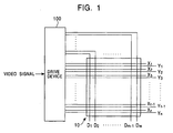
- Fig. 1 is a diagram schematically showing the structure of a plasma display apparatus.
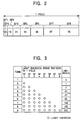
- Fig. 2 shows an example of light emission drive format based on the sub-field method.
- Fig. 3 shows an example of light emission drive pattern.
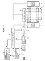
- Fig. 4 shows the structure of a plasma display apparatus which drives a plasma display panel according to the driving method of the present invention.
- Fig. 5 shows the inner structure of a data conversion circuit 30.
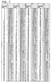
- Fig. 6 shows the data conversion characteristic of a first data conversion circuit 32.
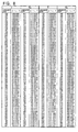
- Fig. 7 shows an example of data conversion table based on the data conversion characteristic shown in Fig. 6.
- Fig. 8 shows an example of data conversion table based on the data conversion characteristic shown in Fig. 6.
- Fig. 9 shows the inner structure of a tone multiplication processing circuit 33.
- Fig. 10 is a drawing for explaining the operation of an error diffusion processing circuit 330.
- Fig. 11 shows the inner structure of a dither processing circuit 350.
- Fig. 12 shows the operation of a dither processing circuit 350.
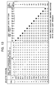
- Fig. 13 shows a first data conversion table used in a second data conversion circuit 34 when the input video signal has a vertical synchronization frequency that is not lower than a predetermined frequency, and a light emission drive pattern thereof.
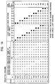
- Fig. 14 shows a second data conversion table used in the second data conversion circuit 34 when the input video signal has a vertical synchronization frequency that is lower than the predetermined frequency, and a light emission drive pattern thereof.
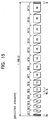
- Fig. 15 shows an example of light emission drive format (based on the selective erasure address method) employed when the input video signal has a vertical synchronization frequency that is not lower than the predetermined frequency.
- Fig. 16 shows an example of light emission drive format (based on the selective erasure address method) employed when the input video signal has a vertical synchronization frequency that is lower than the predetermined frequency.
- Fig. 17 shows the timing of applying various drive pulses to PDP 10.
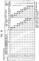
- Fig. 18 shows another example of second data conversion table used in the second data conversion circuit 34 when the input video signal has a vertical synchronization frequency that is lower than the predetermined frequency, and the light emission drive pattern thereof.
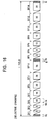
- Fig. 19 shows another example of light emission drive format (based on the selective erasure address method) employed when the input video signal has a vertical synchronization frequency that is lower than the predetermined frequency.
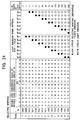
- Fig. 20 shows another example of second data conversion table used in the second data conversion circuit 34 when the input video signal has a vertical synchronization frequency that is lower than the predetermined frequency, and the light emission drive pattern thereof.
- Fig. 21 shows an example of light emission drive format (based on the selective writing address method) employed when the input video signal has a vertical synchronization frequency that is not lower than the predetermined frequency.
- Fig. 22 shows an example of light emission drive format (based on the selective writing address method) employed when the input video signal has a vertical synchronization frequency that is lower than the predetermined frequency.
- Fig. 23 shows the first data conversion table used in the second data conversion circuit 34 when driving according to the light emission drive format shown in Fig. 21, and the light emission drive pattern thereof.
- Fig. 24 shows the second data conversion table used in the second data conversion circuit 34 when driving according to the light emission drive format shown in Fig. 22, and the light emission drive pattern thereof.
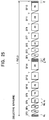
- Fig. 25 shows a variation of the light emission drive format shown in Fig. 16.
- Fig. 26 shows the second data conversion table used in the second data conversion circuit 34 when driving according to the light emission drive format shown in Fig. 25, and the light emission drive pattern thereof.
- Fig. 27 shows a variation of the light emission drive format shown in Fig. 22.
- Fig. 28 shows the second data conversion table used in the second data conversion circuit 34 when driving according to the light emission drive format shown in Fig. 27, and the light emission drive pattern thereof.
- Fig. 29 shows an example of light emission drive pattern employed when dividing one field into 13 sub-fields and driving a toned display based on the selective erasure address method.
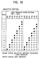
- Fig. 30 shows an example of light emission drive pattern employed when dividing one field into 13 sub-fields and driving a toned display based on the selective writing address technique.
- Fig. 1 shows the schematic structure of a plasma display apparatus which displays pictures with such a plasma display panel.
- PDP 10 which is the plasma display panel has m column electrodes D 1 through D m that serve as data electrodes and n row electrodes X 1 through X n and row electrodes Y 1 through Y n that cross the column electrodes.
- a pair of X and Y electrodes constitute the row electrode corresponding to one line of the screen.
- the column electrode D and the row electrodes X, Y are formed on two glass substrates that are disposed to oppose each other interposing a discharge space which is filled with a discharge gas formed in between. Formed at the intersect of a row electrode and a column electrode is a discharge cell that serves as a display element for one pixel.
- the discharge cell operates by making use of electric discharge, and therefore has only two states of light emitting and non-light emitting. That is, the discharge cell can provide luminance of only two tones, minimum luminance (non-light emitting) and maximum luminance (light emitting). Therefore a drive device 100 drives the PDP 10, comprising the discharge cells arranged in a matrix, by the sub-field method to drive toned display in order to render luminance of an intermediate tone that corresponds to input video signal.
- the sub-field method divides the display period of one field into, for example, eight sub-fields SF1 through SF8 as shown in Fig. 2.
- the number of times light should be turned on in the sub-field is assigned to each of the sub-fields SF1 through SF8.
- light emission is carried out a number of times that corresponding to the luminance level of the input video signal in the display period of one field, by choosing a proper combination of sub-fields where light is to be emitted and sub-fields where light is not to be emitted according to the input video signal. This causes an intermediate level of luminance to be perceived according to the total number of times light is emitted in the display period of one field.
- Fig. 3 shows an example of the combination of sub-fields where light is to be emitted and sub-fields where light is not to be emitted (hereinafter referred to as a light emission drive pattern).
- the drive device 100 selects one of nine different light emission drive patterns shown in Fig. 3, in accordance with the input video signal. Accordingly, various drive pulses are applied to the column electrodes D, and row electrodes X, Y of the PDP 10, to thereby emit light the number of times shown in Fig. 2 only in the sub-fields indicated by white circles in the light emission drive pattern that has been selected.
- pictures can be displayed with nine levels of intermediate luminance having the following proportions of luminance of light emitted. ⁇ 0, 1, 7, 23, 47, 82, 128, 185, 255 ⁇
- the frequency of switching between the sustained light emitting state and the sustained non-light emitting state becomes equal to the vertical synchronization frequency that determines the period of displaying one field.
- Fig. 4 schematically shows the structure of a plasma display apparatus which drives a plasma display panel according to the driving method of the present invention.
- a sync detection circuit 1 when the vertical synchronization frequency is detected from the input video signal, a sync detection circuit 1 generates and supplies a vertical synchronization detection signal V to a drive control circuit 2 and a vertical synchronization frequency detection circuit 3.
- the sync detection circuit 1 When the horizontal synchronization signal is detected from the input video signal, the sync detection circuit 1 generates and supplies a horizontal synchronization detection signal H to the drive control circuit 2.
- the vertical synchronization frequency detection circuit 3 determines the vertical synchronization frequency of the input video signal by measuring the frequency of the vertical synchronization detection signal V, and supplies a vertical synchronization frequency signal VF that represents the frequency to the drive control circuit 2 and a data conversion circuit 30.
- An A/D converter 4 samples the input video signal thereby converting it into, for example, 8-bit pixel data D for each pixel in accordance with a clock signal supplied from the drive control circuit 2, and supplies the pixel data to the data conversion circuit 30.
- Fig. 5 shows the inner structure of a data conversion circuit 30.
- a first data conversion circuit 32 supplies a tone multiplication processing circuit 33 with converted pixel data D 11 that is generated by multiplying the pixel data D by (14 ⁇ 16)/255 according to the conversion characteristic shown in Fig. 6.
- the first data conversion circuit 32 converts the pixel data D that is capable of representing the levels of luminance for 256 tones, from 0 to 255, with eight bits, into the converted pixel data D H that is capable of representing the levels of luminance for 255 tones, from 0 to 224, with eight bits.
- the first data conversion circuit 32 converts the pixel data D into the converted pixel data D H according to the conversion table shown in Fig. 7 and Fig. 8 based on the conversion characteristic shown in Fig. 6.
- the conversion characteristic is determined in accordance with the number of bits of the pixel data, the number of bits compressed in a tone multiplication process to be described later, and the number of displayed tones.
- the data are converted in the first data conversion circuit 32 in consideration of the number of displayed tones and the number of bits compressed in the tone multiplication, before carrying out the tone multiplication process that will be described later.
- the input pixel data D is divided into a group of most significant bits (corresponding to multi-toned pixel data) and a group of least significant bits (data to be discarded: error data), and the tone multiplication process is carried out according to this signal. This makes it possible to prevent saturation of luminance from occurring due to the tone multiplication process and flattening of the display characteristic (that is, distortion of tone) that occurs when the display tone is not on the bit boundary.
- Fig. 9 shows the inner structure of the tone multiplication processing circuit 33 that carries out the tone multiplication process.
- the tone multiplication processing circuit 33 is composed of an error diffusion processing circuit 330 and a dither processing circuit 350.
- a data separation circuit 331 of the error diffusion processing circuit 330 separates the 8-bit converted pixel data D H supplied from the first data conversion circuit 32 into error data consisting of the least significant two bits and display data consisting of the most significant six bits.
- An adder 332 adds the error data, delayed output of a delay circuit 334 and multiplied output of a coefficient multiplier 335, and supplies the sum to a delay circuit 336.
- the delay circuit 336 sends the sum supplied from the adder 332, with a delay time corresponding to the period of one clock cycle of the pixel data (hereinafter called the delay time D) being applied thereto, as delayed addition signal AD 1 to the coefficient multiplier 335 and the delay circuit 337.
- the coefficient multiplier 335 multiplies the delayed addition signal AD 1 by a predetermined coefficient K 1 (7/16, for example) and sends the product to the adder 332.
- the delay circuit 337 sends the delayed addition signal AD 1 , with an additional delay time of (one horizontal scan period - delay time D ⁇ 4) applied thereto, as delayed addition signal AD 2 to a delay circuit 338.
- the delay circuit 338 sends the delayed addition signal AD 2 , with further additional delay time of the delay time D applied thereto, as delayed addition signal AD 3 to a coefficient multiplier 339.
- the delay circuit 338 also sends the delayed addition signal AD 2 , with a delay time of the delay time D ⁇ 2 applied thereto, as delayed addition signal AD 4 to a coefficient multiplier 340.
- the delay circuit 338 further sends the delayed addition signal AD 2 , with a delay time equal to the delay time D ⁇ 3 applied thereto, as a delayed addition signal AD 5 to a coefficient multiplier 341.
- the coefficient multiplier 339 multiplies the delayed addition signal AD 3 by a predetermined coefficient K 2 (3/16, for example) and sends the product to the adder 342.
- the coefficient multiplier 340 multiplies the delayed addition signal AD 4 by a predetermined coefficient K 3 (5/16, for example) and sends the product to the adder 342.
- the coefficient multiplier 341 multiplies the delayed addition signal AD 5 by a predetermined coefficient K 4 (1/16, for example) and sends the product to the adder 342.
- the adder 342 adds up the products supplied from the coefficient multipliers 339, 340 and 341 and sends the sum to the delay circuit 334.
- the delay circuit 334 outputs the addition signal, with the delay time D applied thereto, to the adder 332.
- the adder 332 adds the error data, the delayed output from the delay circuit 334 and the multiplication output from the coefficient multiplier 335, and sends it to an adder 333 a carry-out signal C o having a logical value of 0 when there is no carry over in the addition, or a logical value of 1 when there is carry over in the addition.
- the adder 333 adds the carry-out signal C o to the display data comprising the most significant six bits of the converted pixel data D H and outputs the sum as the 6-bit error diffusion processed pixel data ED.
- the least significant two bits of the converted pixel data HD P namely the error data of the pixel G(j, k)
- the carry-out signal C o consisting of one bit thus obtained is added to the most significant six bits of the converted pixel data D H , namely the display data of the pixel G(j, k), with the result of addition being taken as the error diffusion processed pixel data ED.
- the most significant six bits and the least significant two bits of the converted pixel data D H are used as the display data and the error data, respectively, and the error data weighted by the corresponding weighting factors for the peripheral pixels [G(j, k-1), G(j-1, k+1), G(j-1, k), G(j-1, k-1)] are added, with the result being reflected on the display data.
- This operation causes the luminance corresponding to the least significant two bits at the pixel G(j, k) to be represented alternatively by the peripheral pixels, thereby making it possible to provide a toned representation of luminance equivalent to 8-bit pixel data, by using 6-bit display data which is lower than 8-bit display data.
- the dither processing circuit 350 applies dither process to the error diffusion processed pixel data ED supplied from the error diffusion processing circuit 330.
- one intermediate display level is represented by a plurality of adjacent pixels. For example, to provide a toned display equivalent to that of eight bits by using the pixel data of the most significant six bits among the 8-bit pixel data, four vertically and horizontally adjacent pixels are grouped as a set, and four dither coefficients a through d of different values are added to the pixel data of corresponding pixels of the set.
- the dither process produces four different combinations of intermediate display levels from the four pixels. As a result, even when the pixel data comprises six bits, a number of tone levels four times larger, namely intermediate tones equivalent to those of eight bits, can be represented.
- the dither coefficients a though d to be assigned to the four pixels are changed from field to field.
- Fig. 11 shows the inner structure of the dither processing circuit 350.
- a dither coefficient generation circuit 352 generates four dither coefficients a, b, c and d for the four adjacent pixels [G(j, k), G(j, k+1), G(j+1, k), G(j+1, k+1)] as shown in Fig. 12 and sends the coefficients successively to the adder 351.
- the dither coefficient generation circuit 352 also changes the assignment of the dither coefficients a through d, that are generated in correspondence to the four pixels, from field to field as shown in Fig. 12.
- the dither coefficients a through d are generated cyclically and repetitively for the following assignments and are supplied to the adder 351.
- the dither coefficient generation circuit 352 repetitively carries out the above operation for the first field through the fourth field. That is, when the operation of generating the dither coefficients for the fourth field is completed, the operation is repeated from the first field.
- the adder 351 adds the dither coefficients a through d, that are assigned for each field as described above, to the error diffusion processed pixel data ED of the pixel G(j, k), pixel G(j, k+1), pixel G(j+1, k) and pixel G(j+1, k+1), respectively, that are supplied from the error diffusion processing circuit 330, and supplies the dither-added pixel data thus obtained to an upper bit extraction circuit 353.
- the following values are supplied successively to the upper bit extraction circuit 353 as the dither-added pixel data.
- the upper bit extraction circuit 353 extracts the four most significant bits of the dither-added pixel data, and supplies the extracted data as the multi-toned pixel data D s to the second data conversion circuit 34 shown in Fig. 5.
- the second data conversion circuit 34 converts the multi-toned pixel data D s into 14-bit pixel drive data GD in accordance with a conversion table that corresponds to the vertical synchronization frequency of the input video signal indicated by the vertical synchronization frequency signal VF.
- a conversion table that corresponds to the vertical synchronization frequency of the input video signal indicated by the vertical synchronization frequency signal VF.
- the second data conversion circuit 34 converts the multi-toned pixel data D s into pixel drive data GD in accordance with the first conversion table shown in Fig. 13.
- the multi-toned pixel data Ds is converted into pixel drive data GD in accordance with the second conversion table shown in Fig. 14.
- a memory 5 shown in Fig. 4 stores the pixel drive data GD successively written therein according to the writing signal supplied from the drive control circuit 2.
- the pixel drive data GD 11-nm of one screen frame are read successively from the memory 5 at the same bit digit for one line, and are sent to an address driver 6.
- the pixel drive data bits GD1 11-nm through GD14 11-nm in the memory 5 are determined for each bit digit of the pixel drive data GD 11-nm of one screen frame as follows.
- DB1 11-nm through DB14 11-nm are read off successively line by line according to a read signal supplied from the drive control circuit 2 and supplied to the address driver 6.
- the drive control circuit 2 employs a light emission drive format that corresponds to the vertical synchronization frequency of the input video signal indicated by the vertical synchronization frequency signal VF. According to the light emission drive format that is employed, the drive control circuit 2 generates various timing signals for the control of the address driver 6, a first sustain driver 7 and a second sustain driver 8.
- the drive control circuit 2 when NTSC system television signal having a vertical synchronization frequency of 60Hz or higher is supplied as the input video signal, the drive control circuit 2 employs the light emission drive format shown in Fig. 15. When a signal having vertical synchronization frequency lower than 60Hz, such as a PAL system television signal, is supplied as the input video signal, on the other hand, the drive control circuit 2 employs the light emission drive format shown in Fig. 16.
- the display period for one field (this includes also one frame hereinafter) is divided into 14 sub-fields SF1 through SF 14. And in each sub-field, pixel data writing process Wc where the pixel data is written for each discharge cell of the PDP 10 thereby to set the light emitting cells and non-light emitting cells, and light emission sustaining process Ic where only the cells to be light emitting are turned on to emit light repetitively for the period shown in the drawing, are carried out.- Also a total reset process Rc, where the amounts of charges on the walls of all discharge cells of the PDP 10 are initialized, is carried out in the first sub-field SF1, and erasure process E where charges on the walls of all discharge cells are eliminated is carried out in the last sub-field SF14.
- the sub-fields SF1, SF3, SF5, SF7, SF9, SF11 and SF13 in the light emission drive format of Fig. 15 are executed in the first half of one field, while SF2, SF4, SF6, SF8, SF10, SF12 and SF14 are executed in the second half of the field.
- the erasure process E is carried out in the last sub-field SF13 of the first half, and the total reset process Rc is carried out in the first sub-field SF2 of the second half.
- the address driver 6, the first sustain driver 7 and the second sustain driver 8 apply various drive pulses for achieving the processes described above to the electrodes of the PDP 10 at the timing determined by a timing signal supplied from the drive control circuit 2.
- Fig. 17 shows the timing of various drive pulses applied by the drivers to the column electrodes D and the row electrodes X, Y in the total reset process Rc, the pixel data writing process Wc, the light emission sustaining process Ic and the erasure process E.
- the first sustain driver 7 and the second sustain driver 8 apply such reset pulses RP X and RP Y as shown in Fig. 17 to the row electrodes X 1 through X n and Y 1 through Y n .
- the reset pulses RP X and RP Y are applied, all discharge cells of the PDP 10 discharge to be reset, so that a predetermined amount of charges deposit uniformly on the wall of every discharge cell. Thus all the discharge cells are reset to the light emitting cells.
- the address driver 6 In the pixel data writing process Wc, the address driver 6 generates pixel data pulse group DP (for one line), that has a voltage corresponding to the logical value of the pixel drive data bit DB which has been supplied from the memory 5, and applies the pulses to the column electrode D 1-m .
- the pixel data writing process Wc of the sub-field SF1 for example, the pixel drive data bit DB1 11-1m that corresponds to the first row is read from the memory 5. Accordingly the address driver 6 generates the pixel data pulse group DP consisting of the pixel data pulses of m pieces corresponding to the logical values of the DB1 11-1m and applies the pixel data pulse group DP to the column electrodes D 1-m .
- the address driver 6 generates the pixel data pulse group DP of m pieces corresponding to the logical values of the DB1 21-2m and applies the pixel data pulse group DP to the column electrodes D 1-m .
- pixel data pulse group DP corresponding to the first through nth lines are applied successively to the column electrodes D 1-m thereafter.
- the address driver 6 generates high voltage pixel data pulses when the logical value of the pixel drive data bit DB is "1", and generates low voltage pixel data pulses (0 volts) when the logical value is "0".
- the second sustaining driver 8 generates negative polarity scan pulse SP as shown in Fig. 17 at the same timing as the timing of applying the pixel data pulse group DP described above.
- the scan pulses are applied to the row electrodes Y 1 through Y n successively.
- electrical discharge selective erasure discharge
- the discharge cell that was initialized to the state of an light emitting cell in the total reset process Rc is changed to the state of an non-light emitting cell by this selective erasure discharge.
- the first sustain driver 7 and the second sustain driver 8 repetitively apply sustaining pulses IP X and IP Y of positive polarity to the row electrodes X 1 through X n and Y 1 through Y n alternately, as shown in Fig. 17.
- Proportions of the length of periods during which the sustaining pulse IP is kept being applied in the light emission sustaining process Ic for the sub-fields SF1 through SF14 are set as follows.
- Sustained discharge is carried out in the discharge cell where charges are formed on the wall thereof, namely the light emitting cells, every time the sustaining pulses IP X and IP Y are applied only. That is, only the discharge cells that were set as light emitting cells in the pixel data writing process Wc repeat to emit light through the sustained discharge during the period determined by the weighting factor of the sub-field described above, thus sustaining the light emitting state. The longer the time in which the light emitting state is sustained, the brighter the display is perceived by the human eyes.
- the second sustain driver 8 In the erasure process E, the second sustain driver 8 generates such an erasure pulse EP of negative polarity as shown in Fig. 17 and applies the pulse to the row electrodes Y 1 through Y n .
- Application of the erasure pulse EP causes erasure discharge to occur in all discharge cells of the PDP 10, so that the charges remaining on the walls of all discharge cells disappear. That is, the erasure discharge forces all the discharge cells of the PDP 10 to turn into non-light emitting cells.
- the first through fourteenth bits of the pixel drive data GD shown in Fig. 13 correspond to the sub-fields SF1 through SF14 shown in Fig. 15, respectively.
- the number of times the state is switched from the sustained light emitting state where light is emitted in consecutive sub-fields to the sustained non-light emitting state where light is not emitted in consecutive sub-fields is one in the display period of one field.
- sum of the periods of time during which light was emitted in the light emission sustaining process Ic of the sub-fields SF1 through SF14 relates to the luminance.
- the first through fourteenth bits of the pixel drive data GD shown in Fig. 14 correspond to the sub-fields SF1 through SF14 shown in Fig. 16 as follows, respectively.
- total reset process Rc is executed not only,in the sub-field SF1 but also in the sub-field SF2.
- the discharge cells are first initialized as the light emitting cells in the sub-field SF1.
- the light emitting cell state is maintained until the selective erasure discharge occurs in the sub-fields indicated by the black circles in Fig. 14.
- the light emission sustaining process Ic of each of the sub-fields (indicated by white circles) that are present while the light emitting cell state is maintained light is emitted for a period determined by the weighting factor of the sub-field.
- the discharge cells turn to non-light emitting cells.
- the discharge cells are initialized to light emitting cells again in the sub-field SF2, and maintain the light emitting cell state until the selective erasure discharge occurs in the sub-fields indicated by the black circles.
- the light emission sustaining process Ic for the sub-fields (indicated by the white circles) subsequent to the sub-field SF2 that are present while the light emitting cell state is maintained, light is emitted for a period determined by the weighting factor of the sub-field.
- the number of times the state is switched, from the sustained light emitting state where light is emitted in consecutive sub-fields to the sustained non-light emitting state where light is not emitted in consecutive sub-fields, is two at maximum in the display period of one field.
- sum of the periods of time during which light was emitted in the light emission sustaining process Ic of the sub-fields SF1 through SF14 relates to the luminance of light emission in one field.
- the selective erasure discharge to change the state of the discharge cells is carried out only once in the period from the time of executing the total reset process Rc to the execution of the next total reset process Rc as indicated by the black circles in Fig. 13 and Fig. 14.
- the sub-fields in which light is emitted continue (sustained light emitting state), while sub-fields in which light is not emitted continue (sustained non-light emitting state).
- the present invention employs a toned display operation as the display period of one field is divided into the first drive period (SF1, SF3, SF5, SF7, SF9, SF11, SF13) of the first half and the second drive period (SF2, SF4, SF6, SF8, SF10, SF12, SF14) of the second half as shown in Fig. 14 and Fig. 16.
- the first drive period light is emitted continuously for a period of time corresponding to the luminance level (first tone to fifteenth tone) of the input video signal, beginning at the start of the first drive period.
- the second drive period In the second drive period, on the other hand, light is emitted continuously for a period of time corresponding to the luminance level (first tone to fifteenth tone) of the input video signal, beginning at the start of the second drive period.
- the number of times the state is switched from the sustained light emitting state where light is emitted in consecutive sub-fields to the sustained non-light emitting state where light is not emitted in consecutive sub-fields is two at maximum in the display period of one field.
- the time interval between the start of light emission in the first drive period to the start of light emission in the second drive period is about one half the display period of one field.
- the frequency of switching between the sustained light emitting state and the sustained non-light emitting state is about twice the vertical synchronization frequency that determines the display period of one field, flicker does not occur even when the PAL system television signal of which vertical synchronization frequency is limited to 50Hz is supplied as the input video signal.
- the selective erasure discharge is carried out only once in the period from the execution of the total reset process Rc to the next execution of the total reset process Rc.
- the selective erasure discharge may not occur normally even when the scan pulse SP and the high-voltage pixel data pulse are, for example, applied simultaneously.
- the second conversion table shown in Fig. 18 may be employed instead of that shown in Fig. 14 for use in the second data conversion table 34, to thereby reliably cause the selective erasure discharge.
- the selective erasure discharge occurs in two consecutive sub-fields as indicated by the black circles in Fig. 18. With this operation, even when the charges on the walls in the discharge cells cannot be eliminated normally by the first selective erasure discharge, the charges on the walls can be eliminated normally by the second selective erasure discharge.
- the sub-fields SF1, SF3, SF5, SF7, SF9, SF11 and SF13 are executed in the first half of one field while SF2, SF4, SF6, SF8, SF10, SF12 and SF14 are executed in the second half thereof, although the present invention is not limited to this scheme.
- Fig. 19 shows a variation of the light emission drive format shown in Fig. 16 devised in consideration of the facts described above.
- sub-fields SF1, SF4, SF5, SF8, SF9, SF12 and SF13 are executed successively in the first half of one field while SF2, SF3, SF6, SF7, SF10, SF11 and SF14 are executed successively in the second half thereof.
- Fig. 20 shows the second data conversion table used in the second data conversion circuit 34 when the light emission drive format shown in Fig. 19 is employed, and the light emission drive pattern thereof.
- the embodiment described above is a case of employing the so-called selective erasure address method wherein all discharge cells are set to the light emitting cell state by forming charges on the walls of all discharge cells, and then the charges are eliminated selectively according to the pixel data for the purpose of writing the pixel data.
- the present invention may also be applied to a case of employing the so-called selective writing address method wherein the charges are formed on the wall selectively according to the pixel data for the purpose of writing the pixel data.
- Fig. 21 and Fig. 22 show the light emission drive format used when employing the selective writing address method.
- Fig. 23 shows the first data conversion table used in the second data conversion circuit 34 when the light emission drive format shown in Fig. 21 is employed, and the light emission drive pattern thereof.
- Fig. 24 shows the second data conversion table used in the second data conversion circuit 34 when the light emission drive format shown in Fig. 22 is employed, and the light emission drive pattern thereof.
- toned display is driven in the order of sub-fields from SF14 to SF1, contrary to the case of the light emission drive format shown in Fig. 15.
- the total reset process Rc' where charges remaining on walls of all the discharge cells are eliminated at the same time thereby initializing all discharge cells to the non-light emitting cell state, is carried out only in the first sub-field SF14.
- the pixel data writing process Wc and the light emission sustaining process Ic are carried out in each sub-field.
- sub-fields SF13, SF11, SF9, SF7, SF5, SF3 and SF1 are executed successively in the first half of one field while SF14, SF12, SF10, SF8, SF6, SF4 and SF2 are executed successively in the second half thereof.
- the total reset process Rc' described above is carried out similarly in the first sub-field SF13 of the first half and in the first sub-field SF14 of the second half.
- the pixel data writing process Wc' described above and the light emission sustaining process Ic are carried out in each sub-field.
- the drive control circuit 2 controls the operation according to the light emission drive format shown in Fig. 21 by using the pixel drive data GD shown in Fig. 23.
- the drive control circuit 2 controls the operation according to the light emission drive format shown in Fig. 22 by using the pixel drive data GD shown in Fig. 24.
- the sub-fields having odd numbers are executed in the first half of one field and the sub-fields having even numbers are executed in the second half, although this order may be reverted.
- Fig. 25 shows a variation of the light emission drive format (selective erasure address) shown in Fig. 16 devised in consideration of the facts described above.
- the sub-fields SF2, SF4, SF6, SF8, SF10, SF12 and SF14 wherein light is to be emitted a number of times in proportions of [3: 8: 13: 19: 25: 32: 39] in the respective light emission sustaining process Ic are executed successively in the first half of one field.
- the sub-fields SF1, SF3, SF5, SF7, SF9, SF11 and SF13 wherein light is to be emitted a number of times in proportions of [1: 5: 10: 16: 22: 28: 35] in the respective light emission sustaining process Ic are executed successively.
- Fig. 26 shows the second data conversion table used in the second data conversion circuit 34 when the light emission drive format shown in Fig. 25 is employed, and the light emission drive pattern thereof.
- Fig. 27 shows a variation of the light emission drive format (selective writing address) shown in Fig. 22.
- the sub-fields SF14, SF12, SF10, SF8, SF6, SF4 and SF2 wherein light is to be emitted a number of times in proportions of [39: 32: 25: 16: 13: 5: 3] in the respective light emission sustaining process Ic are executed successively in the first half of one field.
- the sub-fields SF13, SF11, SF9, SF7, SF5, SF3 and SF1 wherein light is to be emitted a number of times in proportions of [35: 28: 22: 19: 10: 8: 1] in the respective light emission sustaining process Ic are executed successively.
- Fig. 28 shows the second data conversion table used in the second data conversion circuit 34 when the light emission drive format shown in Fig. 25 is employed, and the light emission drive pattern thereof.
- the number of sub-fields is not limited to 14.
- Fig. 29 and Fig. 30 show examples of light emission drive pattern employed in case one field is divided into 13 sub-fields and the PDP 10 is driven to provide toned display.
- Fig. 29 shows the light emission drive pattern when the selective erasure address method is employed for writing the pixel data.
- the sub-fields SF1, SF3, SF5, SF7, SF9, SF11 and SF13 wherein light is to be emitted a number of times in proportions of [1: 5: 10: 16: 22: 28: 35] in the respective light emission sustaining process Ic are executed successively in the first half of one field.
- the sub-fields SF2, SF4, SF6, SF8, SF10 and SF12 wherein light is to be emitted a number of times in proportions of [3: 8: 13: 19: 25: 32] in the respective light emission sustaining process Ic are executed successively.
- Fig. 30 shows the light emission drive pattern when the selective writing address method is employed for writing the pixel data.
- the sub-fields SF13, SF11, SF9, SF7, SF5, SF3 and SF1 wherein light is to be emitted a number of times in proportions of [35: 28: 22: 16: 10: 5: 1] in the respective light emission sustaining process Ic are executed successively in the first half of one field.
- the sub-fields SF12, SF10, SF8, SF6, SF4 and SF2 wherein light is to be emitted a number of times in proportions of [32: 25: 19: 13: 8: 3] in the respective light emission sustaining process Ic are executed successively.
- the frequency of switching from the sustained non-light emitting state to the sustained light emitting state (or from the sustained light emitting state to the sustained non-light emitting state) in the display period of one field can be set higher than the vertical synchronization frequency.
Landscapes
- Engineering & Computer Science (AREA)
- Physics & Mathematics (AREA)
- Computer Hardware Design (AREA)
- General Physics & Mathematics (AREA)
- Theoretical Computer Science (AREA)
- Power Engineering (AREA)
- Plasma & Fusion (AREA)
- Control Of Indicators Other Than Cathode Ray Tubes (AREA)
- Control Of Gas Discharge Display Tubes (AREA)
- Transforming Electric Information Into Light Information (AREA)
- Control Of El Displays (AREA)
Applications Claiming Priority (2)
| Application Number | Priority Date | Filing Date | Title |
|---|---|---|---|
| JP2000033496A JP3734244B2 (ja) | 2000-02-10 | 2000-02-10 | ディスプレイパネルの駆動方法 |
| JP2000033496 | 2000-02-10 |
Publications (2)
| Publication Number | Publication Date |
|---|---|
| EP1124216A2 true EP1124216A2 (de) | 2001-08-16 |
| EP1124216A3 EP1124216A3 (de) | 2005-10-05 |
Family
ID=18557972
Family Applications (1)
| Application Number | Title | Priority Date | Filing Date |
|---|---|---|---|
| EP00127839A Withdrawn EP1124216A3 (de) | 2000-02-10 | 2000-12-19 | Verfahren zur Ansteuerung einer Anzeigetafel |
Country Status (2)
| Country | Link |
|---|---|
| EP (1) | EP1124216A3 (de) |
| JP (1) | JP3734244B2 (de) |
Cited By (7)
| Publication number | Priority date | Publication date | Assignee | Title |
|---|---|---|---|---|
| WO2004051611A1 (en) * | 2002-11-29 | 2004-06-17 | Koninklijke Philips Electronics N.V. | Subfield driving pixels in a display device |
| EP1600922A1 (de) * | 2004-05-25 | 2005-11-30 | Samsung SDI Co., Ltd. | Plasmaanzeigevorrichtung und Verfahren zur Ansteuerung eines Plasma-Bildschirms |
| EP1669970A1 (de) * | 2004-12-13 | 2006-06-14 | Samsung SDI Co., Ltd. | Plasmaanzeigevorrichtung und Verfahren zu ihrer Ansteuerung |
| EP1763007A3 (de) * | 2005-09-07 | 2007-10-17 | Pioneer Corporation | Ansteuerverfahren für eine Anzeigetafel |
| CN100353397C (zh) * | 2004-06-04 | 2007-12-05 | 友达光电股份有限公司 | 等离子体显示器和驱动方法 |
| US7773161B2 (en) | 2000-11-30 | 2010-08-10 | Thomson Licensing | Method and apparatus for controlling a display device |
| EP1801770A3 (de) * | 2005-12-20 | 2016-06-22 | Thomson Licensing | Verfahren und Vorrichtung zur Verarbeitung von Videobildern |
Families Citing this family (2)
| Publication number | Priority date | Publication date | Assignee | Title |
|---|---|---|---|---|
| JP4828840B2 (ja) | 2004-07-08 | 2011-11-30 | パナソニック株式会社 | 表示パネルの駆動方法 |
| EP1679680A1 (de) * | 2005-01-06 | 2006-07-12 | Deutsche Thomson-Brandt Gmbh | Verfahren und Vorrichtung zur Verminderung des Grossflächenflimmerns von Videobildern |
Family Cites Families (6)
| Publication number | Priority date | Publication date | Assignee | Title |
|---|---|---|---|---|
| DE69524502T2 (de) * | 1994-07-25 | 2002-06-06 | Texas Instruments Inc | Verfahren zum Reduzieren zeitlicher Artefakte in digitalen Videosystemen |
| JP3322809B2 (ja) * | 1995-10-24 | 2002-09-09 | 富士通株式会社 | ディスプレイ駆動方法及び装置 |
| US5818419A (en) * | 1995-10-31 | 1998-10-06 | Fujitsu Limited | Display device and method for driving the same |
| KR100234034B1 (ko) * | 1996-10-01 | 1999-12-15 | 구자홍 | Ac 플라즈마 디스플레이 판넬 구동방법 |
| JP2962253B2 (ja) * | 1996-12-25 | 1999-10-12 | 日本電気株式会社 | プラズマディスプレイ装置 |
| US6614413B2 (en) * | 1998-04-22 | 2003-09-02 | Pioneer Electronic Corporation | Method of driving plasma display panel |
-
2000
- 2000-02-10 JP JP2000033496A patent/JP3734244B2/ja not_active Expired - Fee Related
- 2000-12-19 EP EP00127839A patent/EP1124216A3/de not_active Withdrawn
Non-Patent Citations (1)
| Title |
|---|
| None |
Cited By (7)
| Publication number | Priority date | Publication date | Assignee | Title |
|---|---|---|---|---|
| US7773161B2 (en) | 2000-11-30 | 2010-08-10 | Thomson Licensing | Method and apparatus for controlling a display device |
| WO2004051611A1 (en) * | 2002-11-29 | 2004-06-17 | Koninklijke Philips Electronics N.V. | Subfield driving pixels in a display device |
| EP1600922A1 (de) * | 2004-05-25 | 2005-11-30 | Samsung SDI Co., Ltd. | Plasmaanzeigevorrichtung und Verfahren zur Ansteuerung eines Plasma-Bildschirms |
| CN100353397C (zh) * | 2004-06-04 | 2007-12-05 | 友达光电股份有限公司 | 等离子体显示器和驱动方法 |
| EP1669970A1 (de) * | 2004-12-13 | 2006-06-14 | Samsung SDI Co., Ltd. | Plasmaanzeigevorrichtung und Verfahren zu ihrer Ansteuerung |
| EP1763007A3 (de) * | 2005-09-07 | 2007-10-17 | Pioneer Corporation | Ansteuerverfahren für eine Anzeigetafel |
| EP1801770A3 (de) * | 2005-12-20 | 2016-06-22 | Thomson Licensing | Verfahren und Vorrichtung zur Verarbeitung von Videobildern |
Also Published As
| Publication number | Publication date |
|---|---|
| JP3734244B2 (ja) | 2006-01-11 |
| JP2001222250A (ja) | 2001-08-17 |
| EP1124216A3 (de) | 2005-10-05 |
Similar Documents
| Publication | Publication Date | Title |
|---|---|---|
| JP3750889B2 (ja) | ディスプレイパネルの中間調表示方法 | |
| JP2001337646A (ja) | プラズマディスプレイパネルの駆動方法 | |
| US6593903B2 (en) | Method for driving a plasma display panel | |
| JP2003015588A (ja) | ディスプレイ装置 | |
| US6483248B2 (en) | Display device | |
| JP4410997B2 (ja) | 表示パネルの駆動装置 | |
| JP2002023693A (ja) | プラズマディスプレイパネルの駆動方法 | |
| JP3961171B2 (ja) | ディスプレイ装置の多階調処理回路 | |
| JP2001337648A (ja) | プラズマディスプレイパネルの駆動方法 | |
| JP3761132B2 (ja) | ディスプレイパネルの駆動方法 | |
| JP2005321442A (ja) | ディスプレイ装置のディザ処理回路 | |
| JP3678401B2 (ja) | プラズマディスプレイパネルの駆動方法 | |
| JPH09218662A (ja) | 自発光画像表示パネルの駆動方法 | |
| EP1124216A2 (de) | Verfahren zur Ansteuerung einer Anzeigetafel | |
| JP4703892B2 (ja) | ディスプレイパネルの駆動方法 | |
| JP2001350447A (ja) | プラズマディスプレイパネルの駆動方法 | |
| JP4071382B2 (ja) | プラズマディスプレイパネルの駆動方法 | |
| JP3644838B2 (ja) | プラズマディスプレイパネルの駆動方法 | |
| JP2003076319A (ja) | プラズマディスプレイパネルの駆動方法 | |
| KR100719084B1 (ko) | 플라즈마 디스플레이 패널, 장치, 패널의 구동 장치 및구동 방법 | |
| JP2000276102A (ja) | プラズマディスプレイパネルの駆動方法 | |
| JP4408350B2 (ja) | 表示パネルの駆動方法 | |
| US7109950B2 (en) | Display apparatus | |
| KR20070101823A (ko) | 플라즈마 디스플레이 패널의 구동 방법 | |
| JP3672292B2 (ja) | プラズマディスプレイパネルの駆動方法 |
Legal Events
| Date | Code | Title | Description |
|---|---|---|---|
| PUAI | Public reference made under article 153(3) epc to a published international application that has entered the european phase |
Free format text: ORIGINAL CODE: 0009012 |
|
| AK | Designated contracting states |
Kind code of ref document: A2 Designated state(s): AT BE CH CY DE DK ES FI FR GB GR IE IT LI LU MC NL PT SE TR |
|
| AX | Request for extension of the european patent |
Free format text: AL;LT;LV;MK;RO;SI |
|
| PUAL | Search report despatched |
Free format text: ORIGINAL CODE: 0009013 |
|
| AK | Designated contracting states |
Kind code of ref document: A3 Designated state(s): AT BE CH CY DE DK ES FI FR GB GR IE IT LI LU MC NL PT SE TR |
|
| AX | Request for extension of the european patent |
Extension state: AL LT LV MK RO SI |
|
| 17P | Request for examination filed |
Effective date: 20050912 |
|
| AKX | Designation fees paid |
Designated state(s): DE FR GB |
|
| RAP1 | Party data changed (applicant data changed or rights of an application transferred) |
Owner name: PANASONIC CORPORATION |
|
| 17Q | First examination report despatched |
Effective date: 20100419 |
|
| STAA | Information on the status of an ep patent application or granted ep patent |
Free format text: STATUS: THE APPLICATION IS DEEMED TO BE WITHDRAWN |
|
| 18D | Application deemed to be withdrawn |
Effective date: 20130702 |