EP1124262A2 - Empilement multicouche des matériaux dielectriques et méthode - Google Patents
Empilement multicouche des matériaux dielectriques et méthode Download PDFInfo
- Publication number
- EP1124262A2 EP1124262A2 EP01301136A EP01301136A EP1124262A2 EP 1124262 A2 EP1124262 A2 EP 1124262A2 EP 01301136 A EP01301136 A EP 01301136A EP 01301136 A EP01301136 A EP 01301136A EP 1124262 A2 EP1124262 A2 EP 1124262A2
- Authority
- EP
- European Patent Office
- Prior art keywords
- dielectric
- layer
- dielectric layer
- dielectric material
- integrated circuit
- Prior art date
- Legal status (The legal status is an assumption and is not a legal conclusion. Google has not performed a legal analysis and makes no representation as to the accuracy of the status listed.)
- Granted
Links
Images

Classifications
-
- H—ELECTRICITY
- H10—SEMICONDUCTOR DEVICES; ELECTRIC SOLID-STATE DEVICES NOT OTHERWISE PROVIDED FOR
- H10P—GENERIC PROCESSES OR APPARATUS FOR THE MANUFACTURE OR TREATMENT OF DEVICES COVERED BY CLASS H10
- H10P10/00—Bonding of wafers, substrates or parts of devices
-
- H—ELECTRICITY
- H10—SEMICONDUCTOR DEVICES; ELECTRIC SOLID-STATE DEVICES NOT OTHERWISE PROVIDED FOR
- H10D—INORGANIC ELECTRIC SEMICONDUCTOR DEVICES
- H10D64/00—Electrodes of devices having potential barriers
- H10D64/01—Manufacture or treatment
- H10D64/013—Manufacture or treatment of electrodes having a conductor capacitively coupled to a semiconductor by an insulator
- H10D64/01302—Manufacture or treatment of electrodes having a conductor capacitively coupled to a semiconductor by an insulator the insulator being formed after the semiconductor body, the semiconductor being silicon
- H10D64/01332—Making the insulator
- H10D64/01336—Making the insulator on single crystalline silicon, e.g. chemical oxidation using a liquid
- H10D64/0134—Making the insulator on single crystalline silicon, e.g. chemical oxidation using a liquid with a treatment, e.g. annealing, after the formation of the insulator and before the formation of the conductor
-
- H—ELECTRICITY
- H10—SEMICONDUCTOR DEVICES; ELECTRIC SOLID-STATE DEVICES NOT OTHERWISE PROVIDED FOR
- H10D—INORGANIC ELECTRIC SEMICONDUCTOR DEVICES
- H10D30/00—Field-effect transistors [FET]
- H10D30/01—Manufacture or treatment
- H10D30/021—Manufacture or treatment of FETs having insulated gates [IGFET]
- H10D30/0223—Manufacture or treatment of FETs having insulated gates [IGFET] having source and drain regions or source and drain extensions self-aligned to sides of the gate
- H10D30/0225—Manufacture or treatment of FETs having insulated gates [IGFET] having source and drain regions or source and drain extensions self-aligned to sides of the gate using an initial gate mask complementary to the prospective gate location, e.g. using dummy source and drain electrodes
-
- H—ELECTRICITY
- H10—SEMICONDUCTOR DEVICES; ELECTRIC SOLID-STATE DEVICES NOT OTHERWISE PROVIDED FOR
- H10D—INORGANIC ELECTRIC SEMICONDUCTOR DEVICES
- H10D64/00—Electrodes of devices having potential barriers
- H10D64/01—Manufacture or treatment
- H10D64/013—Manufacture or treatment of electrodes having a conductor capacitively coupled to a semiconductor by an insulator
- H10D64/01302—Manufacture or treatment of electrodes having a conductor capacitively coupled to a semiconductor by an insulator the insulator being formed after the semiconductor body, the semiconductor being silicon
- H10D64/01332—Making the insulator
- H10D64/01336—Making the insulator on single crystalline silicon, e.g. chemical oxidation using a liquid
- H10D64/01342—Making the insulator on single crystalline silicon, e.g. chemical oxidation using a liquid by deposition, e.g. evaporation, ALD or laser deposition
-
- H—ELECTRICITY
- H10—SEMICONDUCTOR DEVICES; ELECTRIC SOLID-STATE DEVICES NOT OTHERWISE PROVIDED FOR
- H10D—INORGANIC ELECTRIC SEMICONDUCTOR DEVICES
- H10D64/00—Electrodes of devices having potential barriers
- H10D64/60—Electrodes characterised by their materials
- H10D64/66—Electrodes having a conductor capacitively coupled to a semiconductor by an insulator, e.g. MIS electrodes
- H10D64/68—Electrodes having a conductor capacitively coupled to a semiconductor by an insulator, e.g. MIS electrodes characterised by the insulator, e.g. by the gate insulator
- H10D64/681—Electrodes having a conductor capacitively coupled to a semiconductor by an insulator, e.g. MIS electrodes characterised by the insulator, e.g. by the gate insulator having a compositional variation, e.g. multilayered
- H10D64/685—Electrodes having a conductor capacitively coupled to a semiconductor by an insulator, e.g. MIS electrodes characterised by the insulator, e.g. by the gate insulator having a compositional variation, e.g. multilayered being perpendicular to the channel plane
-
- H—ELECTRICITY
- H10—SEMICONDUCTOR DEVICES; ELECTRIC SOLID-STATE DEVICES NOT OTHERWISE PROVIDED FOR
- H10D—INORGANIC ELECTRIC SEMICONDUCTOR DEVICES
- H10D64/00—Electrodes of devices having potential barriers
- H10D64/01—Manufacture or treatment
- H10D64/013—Manufacture or treatment of electrodes having a conductor capacitively coupled to a semiconductor by an insulator
- H10D64/01302—Manufacture or treatment of electrodes having a conductor capacitively coupled to a semiconductor by an insulator the insulator being formed after the semiconductor body, the semiconductor being silicon
- H10D64/01332—Making the insulator
- H10D64/01336—Making the insulator on single crystalline silicon, e.g. chemical oxidation using a liquid
- H10D64/01344—Making the insulator on single crystalline silicon, e.g. chemical oxidation using a liquid in a nitrogen-containing ambient, e.g. N2O oxidation
-
- H—ELECTRICITY
- H10—SEMICONDUCTOR DEVICES; ELECTRIC SOLID-STATE DEVICES NOT OTHERWISE PROVIDED FOR
- H10D—INORGANIC ELECTRIC SEMICONDUCTOR DEVICES
- H10D64/00—Electrodes of devices having potential barriers
- H10D64/60—Electrodes characterised by their materials
- H10D64/66—Electrodes having a conductor capacitively coupled to a semiconductor by an insulator, e.g. MIS electrodes
- H10D64/68—Electrodes having a conductor capacitively coupled to a semiconductor by an insulator, e.g. MIS electrodes characterised by the insulator, e.g. by the gate insulator
- H10D64/691—Electrodes having a conductor capacitively coupled to a semiconductor by an insulator, e.g. MIS electrodes characterised by the insulator, e.g. by the gate insulator comprising metallic compounds, e.g. metal oxides or metal silicates
-
- H—ELECTRICITY
- H10—SEMICONDUCTOR DEVICES; ELECTRIC SOLID-STATE DEVICES NOT OTHERWISE PROVIDED FOR
- H10D—INORGANIC ELECTRIC SEMICONDUCTOR DEVICES
- H10D64/00—Electrodes of devices having potential barriers
- H10D64/60—Electrodes characterised by their materials
- H10D64/66—Electrodes having a conductor capacitively coupled to a semiconductor by an insulator, e.g. MIS electrodes
- H10D64/68—Electrodes having a conductor capacitively coupled to a semiconductor by an insulator, e.g. MIS electrodes characterised by the insulator, e.g. by the gate insulator
- H10D64/693—Electrodes having a conductor capacitively coupled to a semiconductor by an insulator, e.g. MIS electrodes characterised by the insulator, e.g. by the gate insulator the insulator comprising nitrogen, e.g. nitrides, oxynitrides or nitrogen-doped materials
Definitions
- the present invention relates generally to integrated circuit (IC) fabrication processes and, more particularly, to a multilayer dielectric stack, and a method for producing such a stack.
- IC integrated circuit
- SiO 2 As the gate dielectric in MOS devices, the thickness of the SiO 2 layer must also decrease to maintain the same capacitance between the gate and channel regions. Thicknesses of less than 2 nanometers (nm) are expected in the future. However, the occurrence of high tunneling current through such thin layers of SiO 2 requires that alternate materials be considered. Materials with high dielectric constants would permit gate dielectric layers to be made thicker, and so alleviate the tunneling current problem. These so-called high-k dielectric films are defined herein as having a high dielectric constant relative to silicon dioxide. Typically, silicon dioxide has a dielectric constant of approximately 4, while it would be desirable to use a gate dielectric material with a dielectric constant of greater than approximately 10.
- high-k dielectrics develop a crystalline structure under normal integrated circuit manufacturing conditions. As a result, the surface of the film is very rough. Surface roughness causes non-uniform electrical fields in the channel region adjacent the dielectric film. Such films are not suitable for the gate dielectrics of MOSFET devices.
- SiO 2 films thinner than 1.5 nm generally cannot be used as the gate dielectric in CMOS devices.
- TiO 2 and Ta 2 O 5 attracting the greatest -attention.
- high temperature post deposition annealing, and the formation of an interfacial SiO 2 layer make achieving equivalent SiO 2 thicknesses, also known as equivalent oxide thickness (EOT), of less than 1.5 nm very difficult.
- EOT equivalent oxide thickness
- a high-k dielectric film could be used as an insulating barrier between a gate electrode and the underlying channel region in a MOS transistor.
- high-k dielectric films could be formed with reduced surface roughness, crystallinity, and electrical leakage. It would be advantageous if these non-crystalline high dielectric constant materials could be used in gate dielectrics and storage capacitors of integrated circuits.
- a multilayer dielectric stack composed of alternating layers of high-k material, which have high dielectric constants relative to silicon dioxide, and interposing material.
- the high-k material is selected from titanium oxide (TiO 2 ), zirconium oxide (ZrO 2 ), hafnium oxide (HfO 2 ), tantalum oxide (Ta 2 O 5 ), and barium and strontium titanium oxide ((Ba,Sr)TiO 3 ), preferably zirconium oxide or hafnium oxide.
- the interposing material is selected from aluminum oxide (Al 2 O 3 ), aluminum nitride (AlN), silicon nitride (SiN or Si 3 N 4 ), or silicon dioxide (SiO 2 ), preferably aluminum oxide, aluminum nitride or silicon nitride.
- alternating layers of high-k material and interposing material replace prior art silicon dioxide dielectric layers in integrated circuits.
- Each layer is preferably less than 50 angstroms thick.
- the thin layers of high-k material bounded by interposing material reduces or eliminates the formation of crystalline structures.
- the multiple layers reduce the tunneling current, which allows for better device performance. For a fixed total height, additional layers will reduce tunneling current.
- the overall capacitance of a given height stack will vary depending upon the dielectric constant of both the interposing material and the high-k material.
- the number of layers for a desired total thickness will be limited by the minimum thickness obtainable for each layer, and the device characteristics desired.
- an integrated circuit (IC) structure for an IC comprising a multilayer dielectric stack having a first layer of dielectric material overlying a semiconductor substrate, a second layer of dielectric material overlying the first layer, a third layer composed of the same material as the first layer overlying the second layer, and an electrode overlying the dielectric stack.
- the content of the dielectric stack is as described above.
- the overall thickness of the dielectric stack is preferably between 20 and 200 angstroms.
- the integrated circuit structure is a MOS transistor comprising a gate electrode, a channel region having a top surface underlying the gate electrode, and a gate dielectric stack, which comprises a first dielectric layer comprising a first dielectric material, a second dielectric layer comprising a second dielectric material, and a third dielectric layer comprising the same material as the first dielectric layer, interposed between the gate electrode and the channel region top surface.
- Some aspects of the invention further comprise an oxidation barrier interposed between the silicon substrate and the dielectric stack to prevent oxygen from migrating into the silicon substrate beneath the dielectric stack.
- the interface material is selected from the group consisting of aluminum nitride, silicon nitride, and silicon oxynitride.
- a method is provided to form a multilayer dielectric stack on the semiconductor substrate.
- the method comprises the steps of:
- each dielectric layer is formed by atomic layer deposition, which is sometimes referred to as pulsed CVD, of a precursor followed by oxidation of the precursor to form the desired oxide material.
- atomic layer deposition is preferred, alternative methods of depositing each dielectric layer include sputtering and evaporation.
- the entire dielectric stack is preferably annealed at temperatures between approximately 400 and 900 degrees Celsius to condition the stack, the interfaces between the layers, and the interface with the substrate.
- Subsequent processing can be performed to complete the formation of the IC, including depositing an electrode layer and patterning the electrode layer and underlying multiple dielectric layers to form a multilayer dielectric stack structure.
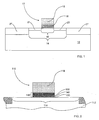
- FIG. 1 is a schematic cross-sectional view showing an integrated circuit structure with a silicon dioxide dielectric layer (prior art).
- FIG. 2 is a schematic cross-sectional view showing an integrated circuit structure with a multilayer dielectric stack.
- FIG. 3 is a schematic cross-sectional view illustrating that the number of layers in the multilayer dielectric stack can be varied.
- FIG. 4 is a schematic cross-sectional view showing an oxidation barrier interposed between a silicon substrate and the multilayer dielectric stack.
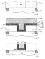
- FIG. 5 is a schematic cross-sectional view showing an intermediate stage following deposition of multiple dielectric layers and an electrode layer.
- FIG. 6 is a schematic cross-sectional view showing an intermediate stage in the formation of a device according to the present invention utilizing a replacement gate method, which illustrates the structure after removal of the preliminary gate.
- FIG. 7 is a schematic cross-sectional view showing an intermediate stage in the formation of a device according to the present invention utilizing a replacement gate method, which illustrates the structure after depositing multiple layers of dielectric material and a layer of electrode material.
- FIG. 8 is a schematic cross-sectional view showing the device of FIG. 7 following a planarization process to remove excess material.
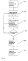
- FIG. 9 is a flow chart summarizing the steps in the method of the present invention.
- FIG. 1 shows a common prior art integrated circuit (IC) structure, specifically a MOS transistor gate structure 10.
- MOS transistor gate structure 10 is formed on a semiconductor substrate 12 above an active area 14 containing a channel region 15.
- MOS transistor gate structure 10 has a silicon dioxide dielectric layer 16 located above channel region 15 having a width.
- An electrode 18, which is typically doped polysilicon, is formed above the dielectric layer 16 to complete the gate structure 10.
- a completed MOS transistor will also include source region 21, drain region 23 and field isolation region 27, which are illustrated in FIG.1 and in some other figures. But, these features will not be further described or identified as they are well known to those skilled in the art. Throughout the remainder of this description structures analogous to the MOS transistor gate structure 10 will often be referred to as an integrated circuit structure to emphasise the applicability of the present invention to other device structures using dielectric materials.
- the thickness of the silicon dioxide dielectric layer 16 must also get smaller to maintain the same capacitance level and other characteristics of the overall device.
- the "size" of IC devices generally refers to the length of the channel region 15. That length is generally equal to the length of the gate electrode 18 as it appears in FIG. 1. As the length continues to shrink the area of the channel region decreases. In order to maintain the capacitance, the thickness of the silicon dioxide layer must decrease. As the necessary thickness of the silicon dioxide dielectric layer becomes very thin, on the order of 20 angstroms, the presence of high tunneling current generally requires use of alternative materials. The alternative materials are referred to as "high-k" materials because they have a high dielectric constant relative to silicon dioxide.
- TiO 2 titanium oxide
- ZrO 2 zirconium oxide
- HfO 2 hafnium oxide
- Ta 2 O 5 tantalum oxide
- Ba,Sr barium and strontium titanium oxide
- the present invention addresses these concerns by using alternating layers of high-k materials, and interposing materials.
- the interposing materials are preferably amorphous. Thin interposing layers separating thin high-k layers reduce or eliminate the formation of polycrystalline structures within the high-k layers. Since the interposing materials are amorphous, they tend to further reduce the amount of crystallization in the adjacent layers. Also by having thin high-k layers, any crystallization that may occur will produce relatively small crystal structures. Although amorphous interposing materials are preferred, single crystal materials, or materials having small polycrystalline structures are also within the scope of the present invention.
- a integrated circuit structure 110 is formed over an active region 114 of an semiconductor substrate 112.
- the integrated circuit structure has a multilayer dielectric stack 116 that replaces silicon dioxide dielectric layer 16, shown in FIG. 1.
- the multilayer dielectric stack has an interposing layer 130 above the active region 114, and a high-k layer 140 above interposing layer 130.
- Interposing layer 130 is composed of aluminum oxide (Al 2 O 3 ), aluminum nitride (AlN), silicon nitride (SiN or Si 3 N 4 ), or silicon dioxide (SiO 2 ), but preferably aluminum oxide.
- Interposing layer 130 is less than 50 angstroms thick.
- High-k layer 140 is composed of a high-k dielectric material.
- the high-k dielectric material is titanium oxide (TiO 2 ), zirconium oxide (ZrO 2 ), hafnium oxide (HfO 2 ), tantalum oxide (Ta 2 O 5 ), or barium and strontium titanium oxide ((Ba,Sr)TiO 3 ), but preferably ZrO 2 , or HfO 2 .
- a second interposing layer 150 overlies the high-k layer 140 and is preferably composed of the same material as interposing layer 130. In a preferred embodiment of the present invention the layers will repeat, for example Al 2 O 3 /ZrO 2 /Al 2 O 3 /ZrO 2 /Al 2 O 3 /ZrO 2.
- the number or pattern of layers could repeat many times. Each additional layer will tend to reduce the tunneling current of the multilayer dielectric stack, while at the same time reducing the overall capacitance . Since it is desirable to have a high capacitance with a low tunneling current, a balance will preferably be determined based on the desired performance of the IC device. It would also be possible to reverse the order of the materials such that high-k layer 140 would be deposited prior to interposing layer 130.
- the topmost layer can be selected to provide good interface with an electrode 118.
- Interposing layer 130 is preferably chosen from a material that will act as an oxidation barrier to protect the underlying silicon. If interposing layer 130 will not act as an oxidation barrier, or if high-k layer 140 would otherwise be in contact with the underlying silicon substrate, an oxidation barrier 170 is provided between semiconductor substrate 112 and multilayer dielectric stack 116, as shown in FIG. 4. Materials that act as oxidation barriers, at the thicknesses required by the present invention, include aluminum oxide, silicon nitride and silicon oxynitride.
- FIG. 5 illustrates an embodiment of an intermediate stage in the production of an integrated circuit structure, with a multilayer dielectric stack 216 according to the present invention.
- Multiple alternating layers of high-k material 230 and interposing material 240 are deposited over an entire wafer 212 to form multilayer dielectric stack 216.
- an electrode layer 218 is also deposited over the entire wafer. Electrode layer 218 and underlying multilayer dielectric stack 216 is patterned and then etched to produce the integrated circuit structure shown in FIG. 2. Additional processes can be performed to produce junctions or other structures as desired.
- the multilayer dielectric stack of the present invention would also be suitable for use in connection with emerging substitute gate manufacturing methods.
- Substitute gates involve the formation of a preliminary gate structure, which is subsequently removed. After the preliminary gate structure is removed, an opening is left where the preliminary gate structure was. A final gate can then be formed in the opening.
- FIG. 6 shows a semiconductor substrate at an intermediate stage in the formation of a substitute gate. The preliminary gate structure has been removed to produce an opening 300 surrounded by a planarization material 311, which is preferably silicon dioxide or silicon nitride.
- FIG. 7 shows a subsequent stage wherein multiple dielectric stack layers 316, formed from alternating layers of interposing material 330 and high-k material 340, and an electrode layer 318 have been deposited over a semiconductor substrate 312 having opening for producing a substitute gate.
- the multilayer dielectric stack layers 316 and electrode layer 318 can be removed from areas where they overly the planarization material 311 by a chemical mechanical polish, or other suitable process, to produce a structure as shown in FIG. 8.
- FIG. 8 shows the present invention applied to a substitute gate structure.
- a multilayer dielectric stack 416 overlays an active area 414. During the formation of multilayer dielectric stack 416, multilayer sidewalls 422 and 424 were also produced.
- An electrode 418, preferably metal, overlays multilayer dielectric stack 416, between multilayer sidewall 422 and 424.
- the steps in the method of the present invention are illustrated schematically in FIG. 9.
- the first step 510 is to provide a semiconductor substrate.
- an oxidation barrier will also be provided overlying the semiconductor substrate.
- Step 520 is the depositing of a thin layer of less than 50 ⁇ of an interposing material, such as aluminum oxide (Al 2 O 3 ), aluminum nitride (AlN), silicon nitride (SiN or Si 3 N 4 ), or silicon dioxide (SiO 2 ) or a high-k material, such titanium oxide (TiO 2 ), zirconium oxide (ZrO 2 ), hafnium oxide (HfO 2 ), tantalum oxide (Ta 2 O 5 ), or barium and strontium titanium oxide ((Ba,Sr)TiO 3 ), but preferably ZrO 2 , or HfO 2 , Preferably, a thin layer of less than 35 angstroms will be deposited. Even thinner layers of less than 20 angstroms would be desirable.
- an interposing material such as aluminum oxide (Al 2 O 3 ), aluminum nitride (AlN), silicon nitride (SiN or Si 3 N 4 ), or silicon dioxide (
- Step 530 is the depositing of a thin layer of less than 50 ⁇ an alternate material either the high-k material or the interposing material, whichever was not deposited in Step 520.
- a thin layer of less than 35 angstroms will be deposited. Even thinner layers of less than 20 angstroms would be desirable.
- Atomic layer deposition also referred to as “pulsed CVD” or “atomic layer epitaxy” is used to deposit an extremely thin layer of material onto the substrate.
- Atomic layer deposition employs a chemical phenomenon known as chemisorption. In chemisorption, a material in a gas phase will adsorb to a surface saturating it, forming a monolayer.
- Most conventional deposition techniques employ physisorption processes, which produce multilayer deposition regions with a surface coverage that is purely statistical. By taking advantage of chemisorption, films can be grown that are extremely uniform in thickness and composition.
- zirconium oxide films have reportedly been grown this way on silicon by using zirconium chloride (ZrCl 4 ) to form the first monolayer, purging the system of ZrCl 4 , and then exposing the surface to water vapor (H 2 O).
- Other precursors for producing zirconium oxide layers include zirconium propoxide (Zr(iOPr) 4 ) and zirconium tetramethyl heptanedionato (Zr(tmhd) 4 ). Chemisorption occurs over a very limited range of temperature and pressures for a given gas-solid combination.
- zirconium oxide has reportedly been deposited on silicon substrates at a temperature of 300 degrees Celsius using ZrCl 4 and H 2 O.
- a layer of interposing material can be formed by depositing one or more monolayers until a desired thickness is reached.
- DMAH dimethyl aluminum hydride
- H 2 O H 2 O 3
- the general processes will need to be optimized, without undue experimentation, to utilize chemisorption in connection with selected precursors.
- the critical aspects of this deposition scheme are sufficient purging from one component prior to introduction of the next component, and the ability to control the temperature and pressure, which may be different for the high-k material and the interposing material.
- Atomic layer deposition makes is possible to produce layers of less than 10 angstroms thick, and preferably layers between approximately 2 and 5 angstroms thick.
- An efficient tool for preparing such ultrathin, atomic layers depositions on semiconductor substrates does not currently exist, although experimental depositions have demonstrated that atomic layer deposition is workable.
- An alternative deposition technique using conventional systems is to sputter targets to lay down a thin layer of high-k or interposing material.
- Two sputtering targets of high purity metal are used. For example, one target of zirconium and one target of aluminum. Each target has its own shutter to control the deposition time.
- a wafer is prepared and placed into a deposition chamber. The wafer is then heated to a temperature between room temperature and 500 degrees Celsius.
- a mixture of argon (Ar) and oxygen (O 2 ) is then introduced into the deposition chamber.
- a plasma with a sputtering power of between approximately 500 W and 5kW is produced within the chamber.
- the shutter for the aluminum target is preferably opened for between approximately 1 and 10 seconds to deposit aluminum over the wafer and then closed.
- the zirconium shutter is opened for between approximately 1 and 20 seconds to deposit zirconium over the wafer, and then closed.
- the presence of oxygen within the chamber will cause the target material to form an oxide concurrently with the deposition on the wafer, producing Al 2 O 3 and ZrO 2 respectively.
- the steps could then be repeated as desired to produce a multiple layer dielectric stack such as Al 2 O 3 /ZrO 2 /Al 2 O 3 /ZrO 2 /Al 2 O 3 /ZrO 2 .
- evaporation of targets is used to deposit the thin layer.
- the basic process is substantially identical to the description provided above with regard to sputtering, except that instead of exposing the targets to a plasma, the targets are heated to a temperature of between approximately 1,000 and 2,000 degrees Celsius.
- shutters can be used to control the duration of the deposition, and alternate between targets.
- the interposing layer is deposited prior to the high-k layer, it would be within the scope of the present invention to deposit the high-k layer first. It is also within the scope of the present invention to produce an uneven number of layers such that the first layer and the last layer can be the same material, or the last layer can be a different material altogether.
- Step 540 provides for the repetition of steps 520 and 530 until the desired number of layers are deposited.
- the deposition of each layer can be controlled by utilizing a shutter, or other means, to control the time of the deposition.
- Step 550 is the annealing of the multilayer dielectric stack in either an inert atmosphere comprising argon, nitrogen or a mixture of nitrogen and hydrogen, or an oxidizing atmosphere comprising oxygen, water vapor, di-nitrogen oxide or nitrous oxide.
- the annealing is preferably performed at an elevated temperature of between 400 and 900 degrees Celsius to condition the high-k layers and the interposing layers as well as the interfaces between the various layers and the interface with the underlying silicon.
- Step 560 is the depositing of an electrode and patterning of the electrode and the underlying multilayer dielectric stack.
- the patterning can be employed with either conventional patterning processes or substitute gate processes as desired.
- the present invention is especially well suited for replacing silicon dioxide as the gate dielectric of a transistor, it would also be useful as a dielectric for storage capacitors, ferroelectric memory devices or other types of integrated circuits.
Landscapes
- Insulated Gate Type Field-Effect Transistor (AREA)
- Formation Of Insulating Films (AREA)
- Semiconductor Memories (AREA)
- Inorganic Insulating Materials (AREA)
- Laminated Bodies (AREA)
Applications Claiming Priority (2)
| Application Number | Priority Date | Filing Date | Title |
|---|---|---|---|
| US09/502,420 US6407435B1 (en) | 2000-02-11 | 2000-02-11 | Multilayer dielectric stack and method |
| US502420 | 2000-02-11 |
Publications (3)
| Publication Number | Publication Date |
|---|---|
| EP1124262A2 true EP1124262A2 (fr) | 2001-08-16 |
| EP1124262A3 EP1124262A3 (fr) | 2002-10-09 |
| EP1124262B1 EP1124262B1 (fr) | 2006-04-19 |
Family
ID=23997739
Family Applications (1)
| Application Number | Title | Priority Date | Filing Date |
|---|---|---|---|
| EP01301136A Expired - Lifetime EP1124262B1 (fr) | 2000-02-11 | 2001-02-08 | Circuit integré comportant un empilement multicouche des matériaux dielectriques et méthode |
Country Status (5)
| Country | Link |
|---|---|
| US (2) | US6407435B1 (fr) |
| EP (1) | EP1124262B1 (fr) |
| JP (1) | JP3912990B2 (fr) |
| KR (1) | KR100419440B1 (fr) |
| DE (1) | DE60118817T2 (fr) |
Cited By (43)
| Publication number | Priority date | Publication date | Assignee | Title |
|---|---|---|---|---|
| JP2003100908A (ja) * | 2001-09-14 | 2003-04-04 | Hynix Semiconductor Inc | 高誘電膜を備えた半導体素子及びその製造方法 |
| DE10153288A1 (de) * | 2001-10-31 | 2003-05-15 | Infineon Technologies Ag | Herstellungsverfahren für ein Halbleiterbauelement |
| EP1324378A1 (fr) * | 2001-12-31 | 2003-07-02 | Memscap | Structure multicouche, utilisée notamment en tant que matériau de forte permittivité relative |
| EP1324379A1 (fr) * | 2001-12-31 | 2003-07-02 | Memscap | Structure multicouche utilisée notamment en tant que matériau de forte permittivité relative |
| WO2003058695A1 (fr) * | 2001-12-27 | 2003-07-17 | Advanced Micro Devices, Inc. | Preparation de chaine de dielectriques de grille a constante k elevee avec couche nitruree |
| US6607973B1 (en) * | 2002-09-16 | 2003-08-19 | Advanced Micro Devices, Inc. | Preparation of high-k nitride silicate layers by cyclic molecular layer deposition |
| WO2003079451A1 (fr) * | 2002-03-15 | 2003-09-25 | Motorola, Inc., A Corporation Of The State Of Delaware | Dielectrique de grille et son procede de fabrication |
| WO2003081667A1 (fr) * | 2002-03-26 | 2003-10-02 | Matsushita Electric Industrial Co., Ltd. | Dispositif semi-conducteur et procede de production associe |
| WO2003105205A1 (fr) * | 2002-06-05 | 2003-12-18 | Micron Technology, Inc. | Couches dielectriques d'oxyde d'hafnium et d'aluminium |
| FR2842830A1 (fr) * | 2002-07-25 | 2004-01-30 | Memscap | Structure multicouche utilisee notamment en tant que materiau de forte permittivite |
| WO2003069655A3 (fr) * | 2002-02-11 | 2004-03-11 | Memscap | Micro-composant electronique incluant une structure capacitive. |
| WO2004053964A1 (fr) * | 2002-12-10 | 2004-06-24 | Intel Corporation | Procede de fabrication d'un dispositif a semi-conducteur ayant un dielectrique de grille a constante k elevee ultra-mince |
| EP1315215A3 (fr) * | 2001-11-27 | 2004-08-18 | Infineon Technologies AG | Transistor à effet de champ à grille flottante |
| WO2003081687A3 (fr) * | 2002-03-20 | 2004-09-30 | Ibm | Transistor a effet de champ muni d'un nanotube autoaligne et procede de fabrication correspondant |
| WO2005020329A1 (fr) * | 2003-08-15 | 2005-03-03 | Intel Corporation | Alliages de metaux de transition utilisables comme gachette et dispositifs incorporant ces alliages |
| US6884739B2 (en) | 2002-08-15 | 2005-04-26 | Micron Technology Inc. | Lanthanide doped TiOx dielectric films by plasma oxidation |
| US6894369B2 (en) | 2001-03-29 | 2005-05-17 | Fujitsu Limited | Semiconductor device having a high-dielectric gate insulation film and fabrication process thereof |
| US6921702B2 (en) | 2002-07-30 | 2005-07-26 | Micron Technology Inc. | Atomic layer deposited nanolaminates of HfO2/ZrO2 films as gate dielectrics |
| US7166505B2 (en) | 2002-02-22 | 2007-01-23 | Intel Corporation | Method for making a semiconductor device having a high-k gate dielectric |
| US7235501B2 (en) | 2004-12-13 | 2007-06-26 | Micron Technology, Inc. | Lanthanum hafnium oxide dielectrics |
| US7326980B2 (en) | 2002-08-28 | 2008-02-05 | Micron Technology, Inc. | Devices with HfSiON dielectric films which are Hf-O rich |
| US7374964B2 (en) | 2005-02-10 | 2008-05-20 | Micron Technology, Inc. | Atomic layer deposition of CeO2/Al2O3 films as gate dielectrics |
| US7494939B2 (en) | 2004-08-31 | 2009-02-24 | Micron Technology, Inc. | Methods for forming a lanthanum-metal oxide dielectric layer |
| EP1610393A4 (fr) * | 2003-03-24 | 2009-03-04 | Horiba Ltd | Dispositif semiconducteur et procede de fabrication de celui-ci |
| US7508648B2 (en) | 2005-02-08 | 2009-03-24 | Micron Technology, Inc. | Atomic layer deposition of Dy doped HfO2 films as gate dielectrics |
| US7511326B2 (en) | 2005-03-29 | 2009-03-31 | Micron Technology, Inc. | ALD of amorphous lanthanide doped TiOx films |
| US7514316B2 (en) | 2003-03-24 | 2009-04-07 | Fujitsu Microelectronics Limited | Semiconductor device and method of manufacturing the same |
| US7588988B2 (en) | 2004-08-31 | 2009-09-15 | Micron Technology, Inc. | Method of forming apparatus having oxide films formed using atomic layer deposition |
| US7592217B2 (en) | 2004-11-08 | 2009-09-22 | Hynix Semiconductor Inc. | Capacitor with zirconium oxide and method for fabricating the same |
| US7601649B2 (en) | 2004-08-02 | 2009-10-13 | Micron Technology, Inc. | Zirconium-doped tantalum oxide films |
| US7662729B2 (en) | 2005-04-28 | 2010-02-16 | Micron Technology, Inc. | Atomic layer deposition of a ruthenium layer to a lanthanide oxide dielectric layer |
| US7709402B2 (en) | 2006-02-16 | 2010-05-04 | Micron Technology, Inc. | Conductive layers for hafnium silicon oxynitride films |
| US7719065B2 (en) | 2004-08-26 | 2010-05-18 | Micron Technology, Inc. | Ruthenium layer for a dielectric layer containing a lanthanide oxide |
| US7728626B2 (en) | 2002-07-08 | 2010-06-01 | Micron Technology, Inc. | Memory utilizing oxide nanolaminates |
| US7759747B2 (en) | 2006-08-31 | 2010-07-20 | Micron Technology, Inc. | Tantalum aluminum oxynitride high-κ dielectric |
| US7776765B2 (en) | 2006-08-31 | 2010-08-17 | Micron Technology, Inc. | Tantalum silicon oxynitride high-k dielectrics and metal gates |
| US7804144B2 (en) | 2001-12-20 | 2010-09-28 | Micron Technology, Inc. | Low-temperature grown high quality ultra-thin CoTiO3 gate dielectrics |
| US7989362B2 (en) | 2006-08-31 | 2011-08-02 | Micron Technology, Inc. | Hafnium lanthanide oxynitride films |
| US8076249B2 (en) | 2005-03-29 | 2011-12-13 | Micron Technology, Inc. | Structures containing titanium silicon oxide |
| US8278225B2 (en) | 2005-01-05 | 2012-10-02 | Micron Technology, Inc. | Hafnium tantalum oxide dielectrics |
| US8501563B2 (en) | 2005-07-20 | 2013-08-06 | Micron Technology, Inc. | Devices with nanocrystals and methods of formation |
| DE102013109353A1 (de) * | 2013-08-29 | 2015-03-05 | Endress + Hauser Conducta Gesellschaft für Mess- und Regeltechnik mbH + Co. KG | Ionensensitive Schichtstruktur für einen ionensensitiven Sensor und Verfahren zur Herstellung derselben |
| US10937897B2 (en) | 2008-07-31 | 2021-03-02 | Semiconductor Energy Laboratory Co., Ltd. | Semiconductor device and method for manufacturing the same |
Families Citing this family (670)
| Publication number | Priority date | Publication date | Assignee | Title |
|---|---|---|---|---|
| US20040224459A1 (en) * | 1999-07-07 | 2004-11-11 | Matsushita Electric Industrial Co., Ltd. | Layered structure, method for manufacturing the same, and semiconductor element |
| US7554829B2 (en) | 1999-07-30 | 2009-06-30 | Micron Technology, Inc. | Transmission lines for CMOS integrated circuits |
| JP2001257344A (ja) * | 2000-03-10 | 2001-09-21 | Toshiba Corp | 半導体装置及び半導体装置の製造方法 |
| FI117979B (fi) | 2000-04-14 | 2007-05-15 | Asm Int | Menetelmä oksidiohutkalvojen valmistamiseksi |
| WO2002001622A2 (fr) * | 2000-06-26 | 2002-01-03 | North Carolina State University | Nouveaux oxydes non cristallins utilises dans des applications optiques, micro-electroniques, et autres |
| US6458416B1 (en) * | 2000-07-19 | 2002-10-01 | Micron Technology, Inc. | Deposition methods |
| US7192888B1 (en) | 2000-08-21 | 2007-03-20 | Micron Technology, Inc. | Low selectivity deposition methods |
| US7094690B1 (en) * | 2000-08-31 | 2006-08-22 | Micron Technology, Inc. | Deposition methods and apparatuses providing surface activation |
| US6969539B2 (en) | 2000-09-28 | 2005-11-29 | President And Fellows Of Harvard College | Vapor deposition of metal oxides, silicates and phosphates, and silicon dioxide |
| US6660660B2 (en) * | 2000-10-10 | 2003-12-09 | Asm International, Nv. | Methods for making a dielectric stack in an integrated circuit |
| US6602805B2 (en) * | 2000-12-14 | 2003-08-05 | Macronix International Co., Ltd. | Method for forming gate dielectric layer in NROM |
| US6831339B2 (en) * | 2001-01-08 | 2004-12-14 | International Business Machines Corporation | Aluminum nitride and aluminum oxide/aluminum nitride heterostructure gate dielectric stack based field effect transistors and method for forming same |
| US6713846B1 (en) * | 2001-01-26 | 2004-03-30 | Aviza Technology, Inc. | Multilayer high κ dielectric films |
| US6844604B2 (en) * | 2001-02-02 | 2005-01-18 | Samsung Electronics Co., Ltd. | Dielectric layer for semiconductor device and method of manufacturing the same |
| US7371633B2 (en) * | 2001-02-02 | 2008-05-13 | Samsung Electronics Co., Ltd. | Dielectric layer for semiconductor device and method of manufacturing the same |
| US7563715B2 (en) | 2005-12-05 | 2009-07-21 | Asm International N.V. | Method of producing thin films |
| US9139906B2 (en) * | 2001-03-06 | 2015-09-22 | Asm America, Inc. | Doping with ALD technology |
| US20050145959A1 (en) * | 2001-03-15 | 2005-07-07 | Leonard Forbes | Technique to mitigate short channel effects with vertical gate transistor with different gate materials |
| US6908639B2 (en) * | 2001-04-02 | 2005-06-21 | Micron Technology, Inc. | Mixed composition interface layer and method of forming |
| JP2002314072A (ja) * | 2001-04-19 | 2002-10-25 | Nec Corp | 高誘電体薄膜を備えた半導体装置及びその製造方法並びに誘電体膜の成膜装置 |
| US7037862B2 (en) * | 2001-06-13 | 2006-05-02 | Micron Technology, Inc. | Dielectric layer forming method and devices formed therewith |
| US6891231B2 (en) * | 2001-06-13 | 2005-05-10 | International Business Machines Corporation | Complementary metal oxide semiconductor (CMOS) gate stack with high dielectric constant gate dielectric and integrated diffusion barrier |
| US20050040478A1 (en) * | 2001-06-25 | 2005-02-24 | Gerald Lucovsky | Novel non-crystalline oxides for use in microelectronic, optical, and other applications |
| US6852575B2 (en) * | 2001-07-05 | 2005-02-08 | International Business Machines Corporation | Method of forming lattice-matched structure on silicon and structure formed thereby |
| US6933566B2 (en) * | 2001-07-05 | 2005-08-23 | International Business Machines Corporation | Method of forming lattice-matched structure on silicon and structure formed thereby |
| US20030198754A1 (en) * | 2001-07-16 | 2003-10-23 | Ming Xi | Aluminum oxide chamber and process |
| US7368014B2 (en) * | 2001-08-09 | 2008-05-06 | Micron Technology, Inc. | Variable temperature deposition methods |
| US8026161B2 (en) | 2001-08-30 | 2011-09-27 | Micron Technology, Inc. | Highly reliable amorphous high-K gate oxide ZrO2 |
| KR100431740B1 (ko) * | 2001-09-14 | 2004-05-17 | 주식회사 하이닉스반도체 | 고유전막을 구비한 반도체소자 및 그 제조 방법 |
| US6960537B2 (en) | 2001-10-02 | 2005-11-01 | Asm America, Inc. | Incorporation of nitrogen into high k dielectric film |
| US6562491B1 (en) * | 2001-10-15 | 2003-05-13 | Advanced Micro Devices, Inc. | Preparation of composite high-K dielectrics |
| US6559014B1 (en) | 2001-10-15 | 2003-05-06 | Advanced Micro Devices, Inc. | Preparation of composite high-K / standard-K dielectrics for semiconductor devices |
| JP2003152102A (ja) * | 2001-11-15 | 2003-05-23 | Hitachi Ltd | 半導体集積回路装置の製造方法 |
| US6900122B2 (en) | 2001-12-20 | 2005-05-31 | Micron Technology, Inc. | Low-temperature grown high-quality ultra-thin praseodymium gate dielectrics |
| US6504214B1 (en) * | 2002-01-11 | 2003-01-07 | Advanced Micro Devices, Inc. | MOSFET device having high-K dielectric layer |
| US6645882B1 (en) * | 2002-01-17 | 2003-11-11 | Advanced Micro Devices, Inc. | Preparation of composite high-K/standard-K dielectrics for semiconductor devices |
| US6767795B2 (en) | 2002-01-17 | 2004-07-27 | Micron Technology, Inc. | Highly reliable amorphous high-k gate dielectric ZrOXNY |
| TW200306664A (en) * | 2002-02-12 | 2003-11-16 | Matsushita Electric Industrial Co Ltd | Ferroelectric capacitor device |
| US6893984B2 (en) * | 2002-02-20 | 2005-05-17 | Micron Technology Inc. | Evaporated LaA1O3 films for gate dielectrics |
| US6586349B1 (en) | 2002-02-21 | 2003-07-01 | Advanced Micro Devices, Inc. | Integrated process for fabrication of graded composite dielectric material layers for semiconductor devices |
| US6451641B1 (en) * | 2002-02-27 | 2002-09-17 | Advanced Micro Devices, Inc. | Non-reducing process for deposition of polysilicon gate electrode over high-K gate dielectric material |
| JP2003282873A (ja) * | 2002-03-22 | 2003-10-03 | Sony Corp | 半導体装置およびその製造方法 |
| US6750066B1 (en) * | 2002-04-08 | 2004-06-15 | Advanced Micro Devices, Inc. | Precision high-K intergate dielectric layer |
| KR100464650B1 (ko) * | 2002-04-23 | 2005-01-03 | 주식회사 하이닉스반도체 | 이중 유전막 구조를 가진 반도체소자의 캐패시터 및 그제조방법 |
| US7160577B2 (en) | 2002-05-02 | 2007-01-09 | Micron Technology, Inc. | Methods for atomic-layer deposition of aluminum oxides in integrated circuits |
| US7589029B2 (en) | 2002-05-02 | 2009-09-15 | Micron Technology, Inc. | Atomic layer deposition and conversion |
| US7045430B2 (en) | 2002-05-02 | 2006-05-16 | Micron Technology Inc. | Atomic layer-deposited LaAlO3 films for gate dielectrics |
| US6621114B1 (en) * | 2002-05-20 | 2003-09-16 | Advanced Micro Devices, Inc. | MOS transistors with high-k dielectric gate insulator for reducing remote scattering |
| US7205218B2 (en) * | 2002-06-05 | 2007-04-17 | Micron Technology, Inc. | Method including forming gate dielectrics having multiple lanthanide oxide layers |
| US7193893B2 (en) | 2002-06-21 | 2007-03-20 | Micron Technology, Inc. | Write once read only memory employing floating gates |
| US7154140B2 (en) | 2002-06-21 | 2006-12-26 | Micron Technology, Inc. | Write once read only memory with large work function floating gates |
| US6970370B2 (en) * | 2002-06-21 | 2005-11-29 | Micron Technology, Inc. | Ferroelectric write once read only memory for archival storage |
| US6804136B2 (en) * | 2002-06-21 | 2004-10-12 | Micron Technology, Inc. | Write once read only memory employing charge trapping in insulators |
| US6996009B2 (en) | 2002-06-21 | 2006-02-07 | Micron Technology, Inc. | NOR flash memory cell with high storage density |
| US7326988B2 (en) | 2002-07-02 | 2008-02-05 | Matsushita Electric Industrial Co., Ltd. | Semiconductor device and method for fabricating the same |
| US7847344B2 (en) | 2002-07-08 | 2010-12-07 | Micron Technology, Inc. | Memory utilizing oxide-nitride nanolaminates |
| JP2004047503A (ja) * | 2002-07-08 | 2004-02-12 | Fujitsu Ltd | 半導体装置及びその製造方法 |
| US7221017B2 (en) | 2002-07-08 | 2007-05-22 | Micron Technology, Inc. | Memory utilizing oxide-conductor nanolaminates |
| KR100468852B1 (ko) * | 2002-07-20 | 2005-01-29 | 삼성전자주식회사 | 캐패시터 구조체 형성 방법 |
| US6790791B2 (en) | 2002-08-15 | 2004-09-14 | Micron Technology, Inc. | Lanthanide doped TiOx dielectric films |
| KR100475116B1 (ko) * | 2002-11-12 | 2005-03-11 | 삼성전자주식회사 | 산화알루미늄/산화하프늄 복합유전막을 가지는 반도체메모리 소자의 커패시터 및 그 제조 방법 |
| US6897106B2 (en) * | 2002-08-16 | 2005-05-24 | Samsung Electronics Co., Ltd. | Capacitor of semiconductor memory device that has composite Al2O3/HfO2 dielectric layer and method of manufacturing the same |
| KR100450681B1 (ko) | 2002-08-16 | 2004-10-02 | 삼성전자주식회사 | 반도체 메모리 소자의 커패시터 및 그 제조 방법 |
| US7425493B2 (en) * | 2002-08-17 | 2008-09-16 | Samsung Electronics Co., Ltd. | Methods of forming dielectric structures and capacitors |
| US7279392B2 (en) * | 2003-08-04 | 2007-10-09 | Samsung Electronics Co., Ltd. | Thin film structure, capacitor, and methods for forming the same |
| KR100542736B1 (ko) | 2002-08-17 | 2006-01-11 | 삼성전자주식회사 | 원자층 증착법을 이용한 산화막의 형성방법 및 이를이용한 반도체 장치의 캐패시터 형성방법 |
| US6753570B1 (en) * | 2002-08-20 | 2004-06-22 | Advanced Micro Devices, Inc. | Memory device and method of making |
| US7084078B2 (en) | 2002-08-29 | 2006-08-01 | Micron Technology, Inc. | Atomic layer deposited lanthanide doped TiOx dielectric films |
| JP3840207B2 (ja) * | 2002-09-30 | 2006-11-01 | 株式会社東芝 | 絶縁膜及び電子素子 |
| US6686212B1 (en) * | 2002-10-31 | 2004-02-03 | Sharp Laboratories Of America, Inc. | Method to deposit a stacked high-κ gate dielectric for CMOS applications |
| TW569313B (en) * | 2002-11-28 | 2004-01-01 | Univ Nat Chiao Tung | Method for improving properties of high k materials by CF4 plasma pre-treatment |
| US7045406B2 (en) * | 2002-12-03 | 2006-05-16 | Asm International, N.V. | Method of forming an electrode with adjusted work function |
| US6858524B2 (en) * | 2002-12-03 | 2005-02-22 | Asm International, Nv | Method of depositing barrier layer for metal gates |
| US7122414B2 (en) * | 2002-12-03 | 2006-10-17 | Asm International, Inc. | Method to fabricate dual metal CMOS devices |
| US7101813B2 (en) | 2002-12-04 | 2006-09-05 | Micron Technology Inc. | Atomic layer deposited Zr-Sn-Ti-O films |
| US6958302B2 (en) | 2002-12-04 | 2005-10-25 | Micron Technology, Inc. | Atomic layer deposited Zr-Sn-Ti-O films using TiI4 |
| AU2003289764A1 (en) * | 2002-12-09 | 2004-06-30 | Asm America Inc. | Method for forming a dielectric stack |
| KR100447979B1 (ko) * | 2002-12-09 | 2004-09-10 | 주식회사 하이닉스반도체 | 반도체 소자의 게이트 형성방법 |
| US6716695B1 (en) * | 2002-12-20 | 2004-04-06 | Texas Instruments Incorporated | Semiconductor with a nitrided silicon gate oxide and method |
| US20040121566A1 (en) * | 2002-12-23 | 2004-06-24 | Infineon Technologies North America Corp | Method to produce low leakage high K materials in thin film form |
| JP4290421B2 (ja) * | 2002-12-27 | 2009-07-08 | Necエレクトロニクス株式会社 | 半導体装置及びその製造方法 |
| US6762114B1 (en) | 2002-12-31 | 2004-07-13 | Texas Instruments Incorporated | Methods for transistor gate fabrication and for reducing high-k gate dielectric roughness |
| US6750126B1 (en) | 2003-01-08 | 2004-06-15 | Texas Instruments Incorporated | Methods for sputter deposition of high-k dielectric films |
| JP2004241612A (ja) | 2003-02-06 | 2004-08-26 | Fujitsu Ltd | 半導体装置及びその製造方法 |
| US7192892B2 (en) | 2003-03-04 | 2007-03-20 | Micron Technology, Inc. | Atomic layer deposited dielectric layers |
| EP1617467A4 (fr) * | 2003-03-26 | 2009-12-16 | Riken | Procede servant a fabriquer une couche mince isolante dielectrique et materiau isolant dielectrique |
| US7135369B2 (en) | 2003-03-31 | 2006-11-14 | Micron Technology, Inc. | Atomic layer deposited ZrAlxOy dielectric layers including Zr4AlO9 |
| JP4691873B2 (ja) * | 2003-03-31 | 2011-06-01 | 富士通株式会社 | 半導体装置およびその製造方法 |
| US7183186B2 (en) | 2003-04-22 | 2007-02-27 | Micro Technology, Inc. | Atomic layer deposited ZrTiO4 films |
| KR100885910B1 (ko) * | 2003-04-30 | 2009-02-26 | 삼성전자주식회사 | 게이트 적층물에 oha막을 구비하는 비 휘발성 반도체메모리 장치 및 그 제조방법 |
| US6930060B2 (en) * | 2003-06-18 | 2005-08-16 | International Business Machines Corporation | Method for forming a uniform distribution of nitrogen in silicon oxynitride gate dielectric |
| US7049192B2 (en) | 2003-06-24 | 2006-05-23 | Micron Technology, Inc. | Lanthanide oxide / hafnium oxide dielectrics |
| US7192824B2 (en) | 2003-06-24 | 2007-03-20 | Micron Technology, Inc. | Lanthanide oxide / hafnium oxide dielectric layers |
| KR100937988B1 (ko) * | 2003-06-25 | 2010-01-21 | 주식회사 하이닉스반도체 | 반도체 소자의 캐패시터 제조방법 |
| KR100703833B1 (ko) * | 2003-06-30 | 2007-04-05 | 주식회사 하이닉스반도체 | 이중 유전막을 구비한 캐패시터의 제조 방법 |
| JP2005064317A (ja) * | 2003-08-18 | 2005-03-10 | Semiconductor Leading Edge Technologies Inc | 半導体装置 |
| US20050070120A1 (en) * | 2003-08-28 | 2005-03-31 | International Sematech | Methods and devices for an insulated dielectric interface between high-k material and silicon |
| KR100541551B1 (ko) * | 2003-09-19 | 2006-01-10 | 삼성전자주식회사 | 적어도 3층의 고유전막들을 갖는 아날로그 커패시터 및그것을 제조하는 방법 |
| US7157769B2 (en) * | 2003-12-18 | 2007-01-02 | Micron Technology, Inc. | Flash memory having a high-permittivity tunnel dielectric |
| KR100639673B1 (ko) * | 2003-12-22 | 2006-10-30 | 삼성전자주식회사 | 고유전 합금으로 이루어지는 게이트 유전막을 구비하는반도체 소자 및 그 제조 방법 |
| US20050142715A1 (en) * | 2003-12-26 | 2005-06-30 | Fujitsu Limited | Semiconductor device with high dielectric constant insulator and its manufacture |
| US20050242301A1 (en) * | 2004-01-12 | 2005-11-03 | Advanced Light Technologies, Llc, A Corporation Of The State Of California | Targeted radiation treatment using a spectrally selective radiation emitter |
| US20050233477A1 (en) * | 2004-03-05 | 2005-10-20 | Tokyo Electron Limited | Substrate processing apparatus, substrate processing method, and program for implementing the method |
| WO2005088727A1 (fr) * | 2004-03-11 | 2005-09-22 | National University Of Singapore | Structure d'empilement de grille de memoire |
| KR100538096B1 (ko) * | 2004-03-16 | 2005-12-21 | 삼성전자주식회사 | 원자층 증착 방법을 이용하는 커패시터 형성 방법 |
| JP2005277223A (ja) * | 2004-03-25 | 2005-10-06 | National Institute Of Advanced Industrial & Technology | 半導体装置およびその製造方法 |
| KR100568448B1 (ko) * | 2004-04-19 | 2006-04-07 | 삼성전자주식회사 | 감소된 불순물을 갖는 고유전막의 제조방법 |
| US7380586B2 (en) * | 2004-05-10 | 2008-06-03 | Bsst Llc | Climate control system for hybrid vehicles using thermoelectric devices |
| US8183629B2 (en) * | 2004-05-13 | 2012-05-22 | Vishay-Siliconix | Stacked trench metal-oxide-semiconductor field effect transistor device |
| DE102004024665A1 (de) * | 2004-05-18 | 2005-12-15 | Infineon Technologies Ag | Verfahren zum Herstellen von dielektrischen Mischschichten und kapazitives Element und Verwendung derselben |
| US7105889B2 (en) * | 2004-06-04 | 2006-09-12 | International Business Machines Corporation | Selective implementation of barrier layers to achieve threshold voltage control in CMOS device fabrication with high k dielectrics |
| GB0412790D0 (en) * | 2004-06-08 | 2004-07-14 | Epichem Ltd | Precursors for deposition of silicon nitride,silicon oxynitride and metal silicon oxynitrides |
| US7279413B2 (en) * | 2004-06-16 | 2007-10-09 | International Business Machines Corporation | High-temperature stable gate structure with metallic electrode |
| KR100642635B1 (ko) * | 2004-07-06 | 2006-11-10 | 삼성전자주식회사 | 하이브리드 유전체막을 갖는 반도체 집적회로 소자들 및그 제조방법들 |
| US7595538B2 (en) * | 2004-08-17 | 2009-09-29 | Nec Electronics Corporation | Semiconductor device |
| KR100653702B1 (ko) * | 2004-08-26 | 2006-12-04 | 삼성전자주식회사 | 플래시 메모리 소자 및 그 제조 방법 |
| KR100688499B1 (ko) | 2004-08-26 | 2007-03-02 | 삼성전자주식회사 | 결정화 방지막을 갖는 유전막을 포함하는 mim 캐패시터및 그 제조방법 |
| WO2006028215A1 (fr) * | 2004-09-09 | 2006-03-16 | Tokyo Electron Limited | Condensateur a film mince, procede de formation de celui-ci et support d’enregistrement lisible par un ordinateur |
| US7507629B2 (en) * | 2004-09-10 | 2009-03-24 | Gerald Lucovsky | Semiconductor devices having an interfacial dielectric layer and related methods |
| JP4309320B2 (ja) * | 2004-09-13 | 2009-08-05 | 株式会社東芝 | 半導体装置及びその製造方法 |
| US7138680B2 (en) * | 2004-09-14 | 2006-11-21 | Infineon Technologies Ag | Memory device with floating gate stack |
| US7282773B2 (en) * | 2004-09-14 | 2007-10-16 | Advanced Micro Devices Inc. | Semiconductor device with high-k dielectric layer |
| KR100660840B1 (ko) * | 2004-10-08 | 2006-12-26 | 삼성전자주식회사 | 다층의 터널링 장벽층을 포함하는 비휘발성 메모리 소자및 그 제조 방법 |
| US7365389B1 (en) | 2004-12-10 | 2008-04-29 | Spansion Llc | Memory cell having enhanced high-K dielectric |
| US7564108B2 (en) * | 2004-12-20 | 2009-07-21 | Taiwan Semiconductor Manufacturing Company, Ltd. | Nitrogen treatment to improve high-k gate dielectrics |
| KR20060072338A (ko) * | 2004-12-23 | 2006-06-28 | 주식회사 하이닉스반도체 | 유전체막 형성방법 및 이를 이용한 반도체 소자의캐패시터 형성방법 |
| US20060151845A1 (en) * | 2005-01-07 | 2006-07-13 | Shrinivas Govindarajan | Method to control interfacial properties for capacitors using a metal flash layer |
| US7316962B2 (en) * | 2005-01-07 | 2008-01-08 | Infineon Technologies Ag | High dielectric constant materials |
| US20060151822A1 (en) * | 2005-01-07 | 2006-07-13 | Shrinivas Govindarajan | DRAM with high K dielectric storage capacitor and method of making the same |
| KR100703966B1 (ko) * | 2005-01-19 | 2007-04-05 | 삼성전자주식회사 | 미세 전자 소자의 다층 유전막 및 그 제조 방법 |
| US7479425B2 (en) * | 2005-01-20 | 2009-01-20 | Chartered Semiconductor Manufacturing, Ltd | Method for forming high-K charge storage device |
| US7863128B1 (en) | 2005-02-04 | 2011-01-04 | Spansion Llc | Non-volatile memory device with improved erase speed |
| JP4372024B2 (ja) * | 2005-02-14 | 2009-11-25 | 株式会社東芝 | Cmos半導体装置 |
| US7399666B2 (en) | 2005-02-15 | 2008-07-15 | Micron Technology, Inc. | Atomic layer deposition of Zr3N4/ZrO2 films as gate dielectrics |
| US7927933B2 (en) * | 2005-02-16 | 2011-04-19 | Imec | Method to enhance the initiation of film growth |
| US7498247B2 (en) | 2005-02-23 | 2009-03-03 | Micron Technology, Inc. | Atomic layer deposition of Hf3N4/HfO2 films as gate dielectrics |
| US7217643B2 (en) * | 2005-02-24 | 2007-05-15 | Freescale Semiconductors, Inc. | Semiconductor structures and methods for fabricating semiconductor structures comprising high dielectric constant stacked structures |
| US7492001B2 (en) * | 2005-03-23 | 2009-02-17 | Spansion Llc | High K stack for non-volatile memory |
| JP2008536318A (ja) * | 2005-04-07 | 2008-09-04 | アヴィザ テクノロジー インコーポレイテッド | 多層多成分高k膜及びそれを堆積させる方法 |
| US7743614B2 (en) | 2005-04-08 | 2010-06-29 | Bsst Llc | Thermoelectric-based heating and cooling system |
| US7598545B2 (en) * | 2005-04-21 | 2009-10-06 | International Business Machines Corporation | Using metal/metal nitride bilayers as gate electrodes in self-aligned aggressively scaled CMOS devices |
| JP2006310662A (ja) * | 2005-04-28 | 2006-11-09 | Toshiba Corp | 不揮発性半導体メモリ装置 |
| US7294547B1 (en) * | 2005-05-13 | 2007-11-13 | Advanced Micro Devices, Inc. | SONOS memory cell having a graded high-K dielectric |
| JP2006324363A (ja) * | 2005-05-17 | 2006-11-30 | Elpida Memory Inc | キャパシタおよびその製造方法 |
| US7572695B2 (en) | 2005-05-27 | 2009-08-11 | Micron Technology, Inc. | Hafnium titanium oxide films |
| US20060267113A1 (en) * | 2005-05-27 | 2006-11-30 | Tobin Philip J | Semiconductor device structure and method therefor |
| KR100653721B1 (ko) * | 2005-06-30 | 2006-12-05 | 삼성전자주식회사 | 질소주입활성영역을 갖는 반도체소자 및 그 제조방법 |
| KR100717813B1 (ko) | 2005-06-30 | 2007-05-11 | 주식회사 하이닉스반도체 | 나노믹스드 유전막을 갖는 캐패시터 및 그의 제조 방법 |
| JP2007019177A (ja) * | 2005-07-06 | 2007-01-25 | Toshiba Corp | 半導体装置 |
| US8783397B2 (en) | 2005-07-19 | 2014-07-22 | Bsst Llc | Energy management system for a hybrid-electric vehicle |
| KR100724566B1 (ko) * | 2005-07-29 | 2007-06-04 | 삼성전자주식회사 | 다층구조의 게이트 층간 유전막을 갖는 플래시 메모리 소자및 그 제조방법들 |
| US7989290B2 (en) | 2005-08-04 | 2011-08-02 | Micron Technology, Inc. | Methods for forming rhodium-based charge traps and apparatus including rhodium-based charge traps |
| US7446369B2 (en) * | 2005-08-04 | 2008-11-04 | Spansion, Llc | SONOS memory cell having high-K dielectric |
| US7575978B2 (en) | 2005-08-04 | 2009-08-18 | Micron Technology, Inc. | Method for making conductive nanoparticle charge storage element |
| KR100628875B1 (ko) * | 2005-08-19 | 2006-09-26 | 삼성전자주식회사 | 소노스 타입의 비휘발성 메모리 장치 및 그 제조 방법 |
| US8110469B2 (en) | 2005-08-30 | 2012-02-07 | Micron Technology, Inc. | Graded dielectric layers |
| US7410910B2 (en) | 2005-08-31 | 2008-08-12 | Micron Technology, Inc. | Lanthanum aluminum oxynitride dielectric films |
| KR100648860B1 (ko) * | 2005-09-08 | 2006-11-24 | 주식회사 하이닉스반도체 | 유전막 및 그 형성방법과, 상기 유전막을 구비한 반도체메모리 소자 및 그 제조방법 |
| US20070099417A1 (en) | 2005-10-28 | 2007-05-03 | Applied Materials, Inc. | Adhesion and minimizing oxidation on electroless CO alloy films for integration with low K inter-metal dielectric and etch stop |
| KR100670747B1 (ko) | 2005-11-28 | 2007-01-17 | 주식회사 하이닉스반도체 | 반도체소자의 캐패시터 제조 방법 |
| US7824990B2 (en) * | 2005-12-05 | 2010-11-02 | Taiwan Semiconductor Manufacturing Company, Ltd. | Multi-metal-oxide high-K gate dielectrics |
| US7592251B2 (en) * | 2005-12-08 | 2009-09-22 | Micron Technology, Inc. | Hafnium tantalum titanium oxide films |
| US7482651B2 (en) * | 2005-12-09 | 2009-01-27 | Micron Technology, Inc. | Enhanced multi-bit non-volatile memory device with resonant tunnel barrier |
| TWI274379B (en) * | 2005-12-26 | 2007-02-21 | Ind Tech Res Inst | MIM capacitor structure and method of manufacturing the same |
| US7870745B2 (en) | 2006-03-16 | 2011-01-18 | Bsst Llc | Thermoelectric device efficiency enhancement using dynamic feedback |
| US8471390B2 (en) | 2006-05-12 | 2013-06-25 | Vishay-Siliconix | Power MOSFET contact metallization |
| JP2007318012A (ja) * | 2006-05-29 | 2007-12-06 | Nec Electronics Corp | 半導体装置およびその製造方法 |
| US20080001237A1 (en) * | 2006-06-29 | 2008-01-03 | Taiwan Semiconductor Manufacturing Company, Ltd. | Semiconductor device having nitrided high-k gate dielectric and metal gate electrode and methods of forming same |
| US20100155018A1 (en) * | 2008-12-19 | 2010-06-24 | Lakhi Nandlal Goenka | Hvac system for a hybrid vehicle |
| US7727908B2 (en) * | 2006-08-03 | 2010-06-01 | Micron Technology, Inc. | Deposition of ZrA1ON films |
| US7582549B2 (en) | 2006-08-25 | 2009-09-01 | Micron Technology, Inc. | Atomic layer deposited barium strontium titanium oxide films |
| US7605030B2 (en) | 2006-08-31 | 2009-10-20 | Micron Technology, Inc. | Hafnium tantalum oxynitride high-k dielectric and metal gates |
| US7960810B2 (en) | 2006-09-05 | 2011-06-14 | Taiwan Semiconductor Manufacturing Company, Ltd. | Semiconductor device with reliable high-voltage gate oxide and method of manufacture thereof |
| KR101427142B1 (ko) * | 2006-10-05 | 2014-08-07 | 에이에스엠 아메리카, 인코포레이티드 | 금속 규산염 막의 원자층 증착 |
| US8986456B2 (en) | 2006-10-10 | 2015-03-24 | Asm America, Inc. | Precursor delivery system |
| US20080150003A1 (en) * | 2006-12-20 | 2008-06-26 | Jian Chen | Electron blocking layers for electronic devices |
| US7847341B2 (en) | 2006-12-20 | 2010-12-07 | Nanosys, Inc. | Electron blocking layers for electronic devices |
| US8686490B2 (en) * | 2006-12-20 | 2014-04-01 | Sandisk Corporation | Electron blocking layers for electronic devices |
| US20080150004A1 (en) * | 2006-12-20 | 2008-06-26 | Nanosys, Inc. | Electron Blocking Layers for Electronic Devices |
| US20080150009A1 (en) * | 2006-12-20 | 2008-06-26 | Nanosys, Inc. | Electron Blocking Layers for Electronic Devices |
| US20080164582A1 (en) * | 2007-01-05 | 2008-07-10 | Shrinivas Govindarajan | Semiconductor devices and methods of manufacture thereof |
| US20080211065A1 (en) * | 2007-03-02 | 2008-09-04 | Shrinivas Govindarajan | Semiconductor devices and methods of manufacture thereof |
| KR100877100B1 (ko) * | 2007-04-16 | 2009-01-09 | 주식회사 하이닉스반도체 | 비휘발성 메모리 소자 제조 방법 |
| US8368126B2 (en) | 2007-04-19 | 2013-02-05 | Vishay-Siliconix | Trench metal oxide semiconductor with recessed trench material and remote contacts |
| WO2008148042A2 (fr) * | 2007-05-25 | 2008-12-04 | Bsst Llc | Système et procédé pour le chauffage et le refroidissement thermoélectrique distribués |
| JP5037242B2 (ja) * | 2007-07-06 | 2012-09-26 | キヤノンアネルバ株式会社 | 半導体素子の製造方法 |
| US7998820B2 (en) | 2007-08-07 | 2011-08-16 | Taiwan Semiconductor Manufacturing Company, Ltd. | High-k gate dielectric and method of manufacture |
| US7772073B2 (en) * | 2007-09-28 | 2010-08-10 | Tokyo Electron Limited | Semiconductor device containing a buried threshold voltage adjustment layer and method of forming |
| JP5280670B2 (ja) * | 2007-12-07 | 2013-09-04 | ルネサスエレクトロニクス株式会社 | 半導体装置の製造方法 |
| US8383525B2 (en) | 2008-04-25 | 2013-02-26 | Asm America, Inc. | Plasma-enhanced deposition process for forming a metal oxide thin film and related structures |
| US20090278120A1 (en) * | 2008-05-09 | 2009-11-12 | Korea Institute Of Science And Technology | Thin Film Transistor |
| US8076237B2 (en) * | 2008-05-09 | 2011-12-13 | Asm America, Inc. | Method and apparatus for 3D interconnect |
| US7863126B2 (en) * | 2008-05-15 | 2011-01-04 | International Business Machines Corporation | Fabrication of a CMOS structure with a high-k dielectric layer oxidizing an aluminum layer in PFET region |
| US8945675B2 (en) | 2008-05-29 | 2015-02-03 | Asm International N.V. | Methods for forming conductive titanium oxide thin films |
| JP2010073867A (ja) * | 2008-09-18 | 2010-04-02 | Tokyo Electron Ltd | 半導体装置及び半導体装置の製造方法 |
| RU2393587C2 (ru) * | 2008-09-30 | 2010-06-27 | Федеральное государственное бюджетное образовательное учреждение высшего профессионального образования "Национальный исследовательский ядерный университет "МИФИ" (НИЯУ МИФИ) | Способ формирования полевого кмоп транзистора, созданного с использованием диэлектриков на основе оксидов металлов с высоким коэффициентом диэлектрической проницаемости и металлических затворов, и структура полевого кмоп транзистора |
| RU2393586C1 (ru) * | 2008-10-06 | 2010-06-27 | Федеральное государственное бюджетное образовательное учреждение высшего профессионального образования "Национальный исследовательский ядерный университет "МИФИ" (НИЯУ МИФИ) | Способ формирования полевого кмоп транзистора, созданного с использованием диэлектриков на основе оксидов металлов с высоким коэффициентом диэлектрической проницаемости и металлических затворов (варианты) |
| EP2946953A1 (fr) | 2008-10-23 | 2015-11-25 | Bsst Llc | Système cvc multimode à dispositif thermoélectrique |
| US10378106B2 (en) | 2008-11-14 | 2019-08-13 | Asm Ip Holding B.V. | Method of forming insulation film by modified PEALD |
| US8557702B2 (en) * | 2009-02-02 | 2013-10-15 | Asm America, Inc. | Plasma-enhanced atomic layers deposition of conductive material over dielectric layers |
| KR101065060B1 (ko) | 2009-03-25 | 2011-09-15 | 광운대학교 산학협력단 | 전하 트랩형 비휘발성 메모리 |
| US9394608B2 (en) | 2009-04-06 | 2016-07-19 | Asm America, Inc. | Semiconductor processing reactor and components thereof |
| US8071452B2 (en) * | 2009-04-27 | 2011-12-06 | Asm America, Inc. | Atomic layer deposition of hafnium lanthanum oxides |
| US20100327364A1 (en) * | 2009-06-29 | 2010-12-30 | Toshiba America Electronic Components, Inc. | Semiconductor device with metal gate |
| US9478637B2 (en) * | 2009-07-15 | 2016-10-25 | Taiwan Semiconductor Manufacturing Company, Ltd. | Scaling EOT by eliminating interfacial layers from high-K/metal gates of MOS devices |
| US8802201B2 (en) | 2009-08-14 | 2014-08-12 | Asm America, Inc. | Systems and methods for thin-film deposition of metal oxides using excited nitrogen-oxygen species |
| US8883270B2 (en) | 2009-08-14 | 2014-11-11 | Asm America, Inc. | Systems and methods for thin-film deposition of metal oxides using excited nitrogen—oxygen species |
| US8877655B2 (en) | 2010-05-07 | 2014-11-04 | Asm America, Inc. | Systems and methods for thin-film deposition of metal oxides using excited nitrogen-oxygen species |
| WO2011043794A2 (fr) * | 2009-09-29 | 2011-04-14 | Yale University | Dispositifs ferroélectriques comprenant une couche ayant deux configurations stables ou davantage |
| KR101712040B1 (ko) * | 2009-10-20 | 2017-03-03 | 에이에스엠 인터내셔널 엔.브이. | 유전체 막들의 부동태화를 위한 공정들 |
| US9306056B2 (en) | 2009-10-30 | 2016-04-05 | Vishay-Siliconix | Semiconductor device with trench-like feed-throughs |
| US9490179B2 (en) * | 2010-05-21 | 2016-11-08 | Semiconductor Energy Laboratory Co., Ltd. | Semiconductor element and semiconductor device |
| US8420208B2 (en) | 2010-08-11 | 2013-04-16 | Micron Technology, Inc. | High-k dielectric material and methods of forming the high-k dielectric material |
| US8501634B2 (en) | 2011-03-10 | 2013-08-06 | United Microelectronics Corp. | Method for fabricating gate structure |
| US8324118B2 (en) | 2011-03-28 | 2012-12-04 | United Microelectronics Corp. | Manufacturing method of metal gate structure |
| US8952458B2 (en) * | 2011-04-14 | 2015-02-10 | Taiwan Semiconductor Manufacturing Company, Ltd. | Gate dielectric layer having interfacial layer and high-K dielectric over the interfacial layer |
| US9312155B2 (en) | 2011-06-06 | 2016-04-12 | Asm Japan K.K. | High-throughput semiconductor-processing apparatus equipped with multiple dual-chamber modules |
| US9793148B2 (en) | 2011-06-22 | 2017-10-17 | Asm Japan K.K. | Method for positioning wafers in multiple wafer transport |
| US10364496B2 (en) | 2011-06-27 | 2019-07-30 | Asm Ip Holding B.V. | Dual section module having shared and unshared mass flow controllers |
| US10854498B2 (en) | 2011-07-15 | 2020-12-01 | Asm Ip Holding B.V. | Wafer-supporting device and method for producing same |
| US20130023129A1 (en) | 2011-07-20 | 2013-01-24 | Asm America, Inc. | Pressure transmitter for a semiconductor processing environment |
| US8383490B2 (en) | 2011-07-27 | 2013-02-26 | International Business Machines Corporation | Borderless contact for ultra-thin body devices |
| US8440520B2 (en) | 2011-08-23 | 2013-05-14 | Tokyo Electron Limited | Diffused cap layers for modifying high-k gate dielectrics and interface layers |
| US8637381B2 (en) | 2011-10-17 | 2014-01-28 | International Business Machines Corporation | High-k dielectric and silicon nitride box region |
| US9341296B2 (en) | 2011-10-27 | 2016-05-17 | Asm America, Inc. | Heater jacket for a fluid line |
| US9096931B2 (en) | 2011-10-27 | 2015-08-04 | Asm America, Inc | Deposition valve assembly and method of heating the same |
| US9017481B1 (en) | 2011-10-28 | 2015-04-28 | Asm America, Inc. | Process feed management for semiconductor substrate processing |
| WO2013074967A1 (fr) | 2011-11-17 | 2013-05-23 | Gentherm Incorporated | Dispositifs thermoélectriques ayant des matières d'interface et procédés de fabrication de ceux-ci |
| US9167625B2 (en) | 2011-11-23 | 2015-10-20 | Asm Ip Holding B.V. | Radiation shielding for a substrate holder |
| US9005539B2 (en) | 2011-11-23 | 2015-04-14 | Asm Ip Holding B.V. | Chamber sealing member |
| CN107680968B (zh) * | 2011-12-28 | 2022-02-22 | 英特尔公司 | 在三栅极(finfet)工艺上集成多个栅极电介质晶体管的方法 |
| US8633118B2 (en) | 2012-02-01 | 2014-01-21 | Tokyo Electron Limited | Method of forming thin metal and semi-metal layers by thermal remote oxygen scavenging |
| US9202727B2 (en) | 2012-03-02 | 2015-12-01 | ASM IP Holding | Susceptor heater shim |
| US8865538B2 (en) | 2012-03-30 | 2014-10-21 | Tokyo Electron Limited | Method of integrating buried threshold voltage adjustment layers for CMOS processing |
| US8946830B2 (en) | 2012-04-04 | 2015-02-03 | Asm Ip Holdings B.V. | Metal oxide protective layer for a semiconductor device |
| US9006094B2 (en) | 2012-04-18 | 2015-04-14 | International Business Machines Corporation | Stratified gate dielectric stack for gate dielectric leakage reduction |
| US9029253B2 (en) | 2012-05-02 | 2015-05-12 | Asm Ip Holding B.V. | Phase-stabilized thin films, structures and devices including the thin films, and methods of forming same |
| US8728832B2 (en) | 2012-05-07 | 2014-05-20 | Asm Ip Holdings B.V. | Semiconductor device dielectric interface layer |
| TWI562368B (en) * | 2012-05-15 | 2016-12-11 | United Microelectronics Corp | Semiconductor structure and process thereof |
| US9478627B2 (en) * | 2012-05-18 | 2016-10-25 | United Microelectronics Corp. | Semiconductor structure and process thereof |
| CN103456785B (zh) * | 2012-05-31 | 2018-01-02 | 联华电子股份有限公司 | 半导体结构及其制作工艺 |
| US8702944B2 (en) | 2012-06-15 | 2014-04-22 | International Business Machines Corporation | Nanopore device wetting |
| US8933375B2 (en) | 2012-06-27 | 2015-01-13 | Asm Ip Holding B.V. | Susceptor heater and method of heating a substrate |
| US9558931B2 (en) | 2012-07-27 | 2017-01-31 | Asm Ip Holding B.V. | System and method for gas-phase sulfur passivation of a semiconductor surface |
| US9117866B2 (en) | 2012-07-31 | 2015-08-25 | Asm Ip Holding B.V. | Apparatus and method for calculating a wafer position in a processing chamber under process conditions |
| US9659799B2 (en) | 2012-08-28 | 2017-05-23 | Asm Ip Holding B.V. | Systems and methods for dynamic semiconductor process scheduling |
| US9169975B2 (en) | 2012-08-28 | 2015-10-27 | Asm Ip Holding B.V. | Systems and methods for mass flow controller verification |
| FR2995135B1 (fr) * | 2012-09-05 | 2015-12-04 | Commissariat Energie Atomique | Procede de realisation de transistors fet |
| US9021985B2 (en) | 2012-09-12 | 2015-05-05 | Asm Ip Holdings B.V. | Process gas management for an inductively-coupled plasma deposition reactor |
| US9324811B2 (en) | 2012-09-26 | 2016-04-26 | Asm Ip Holding B.V. | Structures and devices including a tensile-stressed silicon arsenic layer and methods of forming same |
| US10714315B2 (en) | 2012-10-12 | 2020-07-14 | Asm Ip Holdings B.V. | Semiconductor reaction chamber showerhead |
| US8865581B2 (en) | 2012-10-19 | 2014-10-21 | Tokyo Electron Limited | Hybrid gate last integration scheme for multi-layer high-k gate stacks |
| US9640416B2 (en) | 2012-12-26 | 2017-05-02 | Asm Ip Holding B.V. | Single-and dual-chamber module-attachable wafer-handling chamber |
| US8894870B2 (en) | 2013-02-01 | 2014-11-25 | Asm Ip Holding B.V. | Multi-step method and apparatus for etching compounds containing a metal |
| US20160376700A1 (en) | 2013-02-01 | 2016-12-29 | Asm Ip Holding B.V. | System for treatment of deposition reactor |
| US9484191B2 (en) | 2013-03-08 | 2016-11-01 | Asm Ip Holding B.V. | Pulsed remote plasma method and system |
| US9589770B2 (en) | 2013-03-08 | 2017-03-07 | Asm Ip Holding B.V. | Method and systems for in-situ formation of intermediate reactive species |
| KR102148338B1 (ko) * | 2013-05-03 | 2020-08-26 | 삼성전자 주식회사 | 반도체 소자 및 이의 제조 방법 |
| US8993054B2 (en) | 2013-07-12 | 2015-03-31 | Asm Ip Holding B.V. | Method and system to reduce outgassing in a reaction chamber |
| US9018111B2 (en) | 2013-07-22 | 2015-04-28 | Asm Ip Holding B.V. | Semiconductor reaction chamber with plasma capabilities |
| US9793115B2 (en) | 2013-08-14 | 2017-10-17 | Asm Ip Holding B.V. | Structures and devices including germanium-tin films and methods of forming same |
| US9396934B2 (en) | 2013-08-14 | 2016-07-19 | Asm Ip Holding B.V. | Methods of forming films including germanium tin and structures and devices including the films |
| US9240412B2 (en) | 2013-09-27 | 2016-01-19 | Asm Ip Holding B.V. | Semiconductor structure and device and methods of forming same using selective epitaxial process |
| US9556516B2 (en) | 2013-10-09 | 2017-01-31 | ASM IP Holding B.V | Method for forming Ti-containing film by PEALD using TDMAT or TDEAT |
| US9605343B2 (en) | 2013-11-13 | 2017-03-28 | Asm Ip Holding B.V. | Method for forming conformal carbon films, structures conformal carbon film, and system of forming same |
| US10179947B2 (en) | 2013-11-26 | 2019-01-15 | Asm Ip Holding B.V. | Method for forming conformal nitrided, oxidized, or carbonized dielectric film by atomic layer deposition |
| US20150187900A1 (en) * | 2013-12-26 | 2015-07-02 | Sadasivan Shankar | Composite materials for use in semiconductor components |
| US10683571B2 (en) | 2014-02-25 | 2020-06-16 | Asm Ip Holding B.V. | Gas supply manifold and method of supplying gases to chamber using same |
| US10167557B2 (en) | 2014-03-18 | 2019-01-01 | Asm Ip Holding B.V. | Gas distribution system, reactor including the system, and methods of using the same |
| US9447498B2 (en) | 2014-03-18 | 2016-09-20 | Asm Ip Holding B.V. | Method for performing uniform processing in gas system-sharing multiple reaction chambers |
| US11015245B2 (en) | 2014-03-19 | 2021-05-25 | Asm Ip Holding B.V. | Gas-phase reactor and system having exhaust plenum and components thereof |
| US9404587B2 (en) | 2014-04-24 | 2016-08-02 | ASM IP Holding B.V | Lockout tagout for semiconductor vacuum valve |
| US9263541B2 (en) * | 2014-04-25 | 2016-02-16 | Globalfoundries Inc. | Alternative gate dielectric films for silicon germanium and germanium channel materials |
| US10038063B2 (en) | 2014-06-10 | 2018-07-31 | International Business Machines Corporation | Tunable breakdown voltage RF FET devices |
| US10858737B2 (en) | 2014-07-28 | 2020-12-08 | Asm Ip Holding B.V. | Showerhead assembly and components thereof |
| US9543180B2 (en) | 2014-08-01 | 2017-01-10 | Asm Ip Holding B.V. | Apparatus and method for transporting wafers between wafer carrier and process tool under vacuum |
| US9890456B2 (en) | 2014-08-21 | 2018-02-13 | Asm Ip Holding B.V. | Method and system for in situ formation of gas-phase compounds |
| US10941490B2 (en) | 2014-10-07 | 2021-03-09 | Asm Ip Holding B.V. | Multiple temperature range susceptor, assembly, reactor and system including the susceptor, and methods of using the same |
| US9657845B2 (en) | 2014-10-07 | 2017-05-23 | Asm Ip Holding B.V. | Variable conductance gas distribution apparatus and method |
| KR102300403B1 (ko) | 2014-11-19 | 2021-09-09 | 에이에스엠 아이피 홀딩 비.브이. | 박막 증착 방법 |
| KR102263121B1 (ko) | 2014-12-22 | 2021-06-09 | 에이에스엠 아이피 홀딩 비.브이. | 반도체 소자 및 그 제조 방법 |
| US9478415B2 (en) | 2015-02-13 | 2016-10-25 | Asm Ip Holding B.V. | Method for forming film having low resistance and shallow junction depth |
| US10529542B2 (en) | 2015-03-11 | 2020-01-07 | Asm Ip Holdings B.V. | Cross-flow reactor and method |
| US10276355B2 (en) | 2015-03-12 | 2019-04-30 | Asm Ip Holding B.V. | Multi-zone reactor, system including the reactor, and method of using the same |
| US10458018B2 (en) | 2015-06-26 | 2019-10-29 | Asm Ip Holding B.V. | Structures including metal carbide material, devices including the structures, and methods of forming same |
| US10600673B2 (en) | 2015-07-07 | 2020-03-24 | Asm Ip Holding B.V. | Magnetic susceptor to baseplate seal |
| US9899291B2 (en) | 2015-07-13 | 2018-02-20 | Asm Ip Holding B.V. | Method for protecting layer by forming hydrocarbon-based extremely thin film |
| US10043661B2 (en) | 2015-07-13 | 2018-08-07 | Asm Ip Holding B.V. | Method for protecting layer by forming hydrocarbon-based extremely thin film |
| US10083836B2 (en) | 2015-07-24 | 2018-09-25 | Asm Ip Holding B.V. | Formation of boron-doped titanium metal films with high work function |
| US10087525B2 (en) | 2015-08-04 | 2018-10-02 | Asm Ip Holding B.V. | Variable gap hard stop design |
| US9647114B2 (en) | 2015-08-14 | 2017-05-09 | Asm Ip Holding B.V. | Methods of forming highly p-type doped germanium tin films and structures and devices including the films |
| US9540729B1 (en) | 2015-08-25 | 2017-01-10 | Asm Ip Holding B.V. | Deposition of titanium nanolaminates for use in integrated circuit fabrication |
| US9523148B1 (en) | 2015-08-25 | 2016-12-20 | Asm Ip Holdings B.V. | Process for deposition of titanium oxynitride for use in integrated circuit fabrication |
| US9711345B2 (en) | 2015-08-25 | 2017-07-18 | Asm Ip Holding B.V. | Method for forming aluminum nitride-based film by PEALD |
| US9960072B2 (en) | 2015-09-29 | 2018-05-01 | Asm Ip Holding B.V. | Variable adjustment for precise matching of multiple chamber cavity housings |
| US11120884B2 (en) | 2015-09-30 | 2021-09-14 | Sunrise Memory Corporation | Implementing logic function and generating analog signals using NOR memory strings |
| US9909214B2 (en) | 2015-10-15 | 2018-03-06 | Asm Ip Holding B.V. | Method for depositing dielectric film in trenches by PEALD |
| US10211308B2 (en) | 2015-10-21 | 2019-02-19 | Asm Ip Holding B.V. | NbMC layers |
| US10322384B2 (en) | 2015-11-09 | 2019-06-18 | Asm Ip Holding B.V. | Counter flow mixer for process chamber |
| US9455138B1 (en) | 2015-11-10 | 2016-09-27 | Asm Ip Holding B.V. | Method for forming dielectric film in trenches by PEALD using H-containing gas |
| US9905420B2 (en) | 2015-12-01 | 2018-02-27 | Asm Ip Holding B.V. | Methods of forming silicon germanium tin films and structures and devices including the films |
| US9607837B1 (en) | 2015-12-21 | 2017-03-28 | Asm Ip Holding B.V. | Method for forming silicon oxide cap layer for solid state diffusion process |
| US9627221B1 (en) | 2015-12-28 | 2017-04-18 | Asm Ip Holding B.V. | Continuous process incorporating atomic layer etching |
| US9735024B2 (en) | 2015-12-28 | 2017-08-15 | Asm Ip Holding B.V. | Method of atomic layer etching using functional group-containing fluorocarbon |
| US11139308B2 (en) | 2015-12-29 | 2021-10-05 | Asm Ip Holding B.V. | Atomic layer deposition of III-V compounds to form V-NAND devices |
| US9754779B1 (en) | 2016-02-19 | 2017-09-05 | Asm Ip Holding B.V. | Method for forming silicon nitride film selectively on sidewalls or flat surfaces of trenches |
| US10468251B2 (en) | 2016-02-19 | 2019-11-05 | Asm Ip Holding B.V. | Method for forming spacers using silicon nitride film for spacer-defined multiple patterning |
| US10529554B2 (en) | 2016-02-19 | 2020-01-07 | Asm Ip Holding B.V. | Method for forming silicon nitride film selectively on sidewalls or flat surfaces of trenches |
| US10501866B2 (en) | 2016-03-09 | 2019-12-10 | Asm Ip Holding B.V. | Gas distribution apparatus for improved film uniformity in an epitaxial system |
| US10343920B2 (en) | 2016-03-18 | 2019-07-09 | Asm Ip Holding B.V. | Aligned carbon nanotubes |
| US9892913B2 (en) | 2016-03-24 | 2018-02-13 | Asm Ip Holding B.V. | Radial and thickness control via biased multi-port injection settings |
| US10865475B2 (en) | 2016-04-21 | 2020-12-15 | Asm Ip Holding B.V. | Deposition of metal borides and silicides |
| US10087522B2 (en) | 2016-04-21 | 2018-10-02 | Asm Ip Holding B.V. | Deposition of metal borides |
| US10190213B2 (en) | 2016-04-21 | 2019-01-29 | Asm Ip Holding B.V. | Deposition of metal borides |
| US10032628B2 (en) | 2016-05-02 | 2018-07-24 | Asm Ip Holding B.V. | Source/drain performance through conformal solid state doping |
| US10367080B2 (en) | 2016-05-02 | 2019-07-30 | Asm Ip Holding B.V. | Method of forming a germanium oxynitride film |
| US10304936B2 (en) | 2016-05-04 | 2019-05-28 | International Business Machines Corporation | Protection of high-K dielectric during reliability anneal on nanosheet structures |
| KR102592471B1 (ko) | 2016-05-17 | 2023-10-20 | 에이에스엠 아이피 홀딩 비.브이. | 금속 배선 형성 방법 및 이를 이용한 반도체 장치의 제조 방법 |
| US11453943B2 (en) | 2016-05-25 | 2022-09-27 | Asm Ip Holding B.V. | Method for forming carbon-containing silicon/metal oxide or nitride film by ALD using silicon precursor and hydrocarbon precursor |
| US10388509B2 (en) | 2016-06-28 | 2019-08-20 | Asm Ip Holding B.V. | Formation of epitaxial layers via dislocation filtering |
| US9859151B1 (en) | 2016-07-08 | 2018-01-02 | Asm Ip Holding B.V. | Selective film deposition method to form air gaps |
| US10612137B2 (en) | 2016-07-08 | 2020-04-07 | Asm Ip Holdings B.V. | Organic reactants for atomic layer deposition |
| US9793135B1 (en) | 2016-07-14 | 2017-10-17 | ASM IP Holding B.V | Method of cyclic dry etching using etchant film |
| US10714385B2 (en) | 2016-07-19 | 2020-07-14 | Asm Ip Holding B.V. | Selective deposition of tungsten |
| US10381226B2 (en) | 2016-07-27 | 2019-08-13 | Asm Ip Holding B.V. | Method of processing substrate |
| US10177025B2 (en) | 2016-07-28 | 2019-01-08 | Asm Ip Holding B.V. | Method and apparatus for filling a gap |
| KR102532607B1 (ko) | 2016-07-28 | 2023-05-15 | 에이에스엠 아이피 홀딩 비.브이. | 기판 가공 장치 및 그 동작 방법 |
| US9812320B1 (en) | 2016-07-28 | 2017-11-07 | Asm Ip Holding B.V. | Method and apparatus for filling a gap |
| US9887082B1 (en) | 2016-07-28 | 2018-02-06 | Asm Ip Holding B.V. | Method and apparatus for filling a gap |
| US10395919B2 (en) | 2016-07-28 | 2019-08-27 | Asm Ip Holding B.V. | Method and apparatus for filling a gap |
| US10090316B2 (en) | 2016-09-01 | 2018-10-02 | Asm Ip Holding B.V. | 3D stacked multilayer semiconductor memory using doped select transistor channel |
| KR102228412B1 (ko) * | 2016-11-03 | 2021-03-17 | 주식회사 원익아이피에스 | 하드 마스크 제조방법 |
| KR102268492B1 (ko) * | 2017-09-22 | 2021-06-25 | 주식회사 원익아이피에스 | 복합막 제조방법 |
| KR102228408B1 (ko) * | 2016-10-06 | 2021-03-17 | 주식회사 원익아이피에스 | 하드 마스크 제조방법 |
| TWI661076B (zh) * | 2016-10-06 | 2019-06-01 | 南韓商圓益Ips股份有限公司 | 複合膜製造方法 |
| US10410943B2 (en) | 2016-10-13 | 2019-09-10 | Asm Ip Holding B.V. | Method for passivating a surface of a semiconductor and related systems |
| US10643826B2 (en) | 2016-10-26 | 2020-05-05 | Asm Ip Holdings B.V. | Methods for thermally calibrating reaction chambers |
| US11532757B2 (en) | 2016-10-27 | 2022-12-20 | Asm Ip Holding B.V. | Deposition of charge trapping layers |
| US10840350B2 (en) * | 2016-10-31 | 2020-11-17 | Taiwan Semiconductor Manufacturing Co., Ltd. | Nanolaminate structure, semiconductor device and method of forming nanolaminate structure |
| US10643904B2 (en) | 2016-11-01 | 2020-05-05 | Asm Ip Holdings B.V. | Methods for forming a semiconductor device and related semiconductor device structures |
| US10435790B2 (en) | 2016-11-01 | 2019-10-08 | Asm Ip Holding B.V. | Method of subatmospheric plasma-enhanced ALD using capacitively coupled electrodes with narrow gap |
| US10229833B2 (en) | 2016-11-01 | 2019-03-12 | Asm Ip Holding B.V. | Methods for forming a transition metal nitride film on a substrate by atomic layer deposition and related semiconductor device structures |
| US10714350B2 (en) | 2016-11-01 | 2020-07-14 | ASM IP Holdings, B.V. | Methods for forming a transition metal niobium nitride film on a substrate by atomic layer deposition and related semiconductor device structures |
| US10134757B2 (en) | 2016-11-07 | 2018-11-20 | Asm Ip Holding B.V. | Method of processing a substrate and a device manufactured by using the method |
| KR102546317B1 (ko) | 2016-11-15 | 2023-06-21 | 에이에스엠 아이피 홀딩 비.브이. | 기체 공급 유닛 및 이를 포함하는 기판 처리 장치 |
| US10340135B2 (en) | 2016-11-28 | 2019-07-02 | Asm Ip Holding B.V. | Method of topologically restricted plasma-enhanced cyclic deposition of silicon or metal nitride |
| KR102762543B1 (ko) | 2016-12-14 | 2025-02-05 | 에이에스엠 아이피 홀딩 비.브이. | 기판 처리 장치 |
| US11581186B2 (en) | 2016-12-15 | 2023-02-14 | Asm Ip Holding B.V. | Sequential infiltration synthesis apparatus |
| US9916980B1 (en) | 2016-12-15 | 2018-03-13 | Asm Ip Holding B.V. | Method of forming a structure on a substrate |
| US11447861B2 (en) | 2016-12-15 | 2022-09-20 | Asm Ip Holding B.V. | Sequential infiltration synthesis apparatus and a method of forming a patterned structure |
| KR102700194B1 (ko) | 2016-12-19 | 2024-08-28 | 에이에스엠 아이피 홀딩 비.브이. | 기판 처리 장치 |
| US10269558B2 (en) | 2016-12-22 | 2019-04-23 | Asm Ip Holding B.V. | Method of forming a structure on a substrate |
| US10867788B2 (en) | 2016-12-28 | 2020-12-15 | Asm Ip Holding B.V. | Method of forming a structure on a substrate |
| US11390950B2 (en) | 2017-01-10 | 2022-07-19 | Asm Ip Holding B.V. | Reactor system and method to reduce residue buildup during a film deposition process |
| US10655221B2 (en) | 2017-02-09 | 2020-05-19 | Asm Ip Holding B.V. | Method for depositing oxide film by thermal ALD and PEALD |
| US10468261B2 (en) | 2017-02-15 | 2019-11-05 | Asm Ip Holding B.V. | Methods for forming a metallic film on a substrate by cyclical deposition and related semiconductor device structures |
| US10283353B2 (en) | 2017-03-29 | 2019-05-07 | Asm Ip Holding B.V. | Method of reforming insulating film deposited on substrate with recess pattern |
| US10529563B2 (en) | 2017-03-29 | 2020-01-07 | Asm Ip Holdings B.V. | Method for forming doped metal oxide films on a substrate by cyclical deposition and related semiconductor device structures |
| US10103040B1 (en) | 2017-03-31 | 2018-10-16 | Asm Ip Holding B.V. | Apparatus and method for manufacturing a semiconductor device |
| USD830981S1 (en) | 2017-04-07 | 2018-10-16 | Asm Ip Holding B.V. | Susceptor for semiconductor substrate processing apparatus |
| KR102457289B1 (ko) | 2017-04-25 | 2022-10-21 | 에이에스엠 아이피 홀딩 비.브이. | 박막 증착 방법 및 반도체 장치의 제조 방법 |
| US10770286B2 (en) | 2017-05-08 | 2020-09-08 | Asm Ip Holdings B.V. | Methods for selectively forming a silicon nitride film on a substrate and related semiconductor device structures |
| US10446393B2 (en) | 2017-05-08 | 2019-10-15 | Asm Ip Holding B.V. | Methods for forming silicon-containing epitaxial layers and related semiconductor device structures |
| US10892156B2 (en) | 2017-05-08 | 2021-01-12 | Asm Ip Holding B.V. | Methods for forming a silicon nitride film on a substrate and related semiconductor device structures |
| US10504742B2 (en) | 2017-05-31 | 2019-12-10 | Asm Ip Holding B.V. | Method of atomic layer etching using hydrogen plasma |
| US10886123B2 (en) | 2017-06-02 | 2021-01-05 | Asm Ip Holding B.V. | Methods for forming low temperature semiconductor layers and related semiconductor device structures |
| US12040200B2 (en) | 2017-06-20 | 2024-07-16 | Asm Ip Holding B.V. | Semiconductor processing apparatus and methods for calibrating a semiconductor processing apparatus |
| US11306395B2 (en) | 2017-06-28 | 2022-04-19 | Asm Ip Holding B.V. | Methods for depositing a transition metal nitride film on a substrate by atomic layer deposition and related deposition apparatus |
| US10685834B2 (en) | 2017-07-05 | 2020-06-16 | Asm Ip Holdings B.V. | Methods for forming a silicon germanium tin layer and related semiconductor device structures |
| KR20190009245A (ko) | 2017-07-18 | 2019-01-28 | 에이에스엠 아이피 홀딩 비.브이. | 반도체 소자 구조물 형성 방법 및 관련된 반도체 소자 구조물 |
| US11374112B2 (en) | 2017-07-19 | 2022-06-28 | Asm Ip Holding B.V. | Method for depositing a group IV semiconductor and related semiconductor device structures |
| US11018002B2 (en) | 2017-07-19 | 2021-05-25 | Asm Ip Holding B.V. | Method for selectively depositing a Group IV semiconductor and related semiconductor device structures |
| US10541333B2 (en) | 2017-07-19 | 2020-01-21 | Asm Ip Holding B.V. | Method for depositing a group IV semiconductor and related semiconductor device structures |
| US10605530B2 (en) | 2017-07-26 | 2020-03-31 | Asm Ip Holding B.V. | Assembly of a liner and a flange for a vertical furnace as well as the liner and the vertical furnace |
| US10312055B2 (en) | 2017-07-26 | 2019-06-04 | Asm Ip Holding B.V. | Method of depositing film by PEALD using negative bias |
| US10590535B2 (en) | 2017-07-26 | 2020-03-17 | Asm Ip Holdings B.V. | Chemical treatment, deposition and/or infiltration apparatus and method for using the same |
| TWI815813B (zh) | 2017-08-04 | 2023-09-21 | 荷蘭商Asm智慧財產控股公司 | 用於分配反應腔內氣體的噴頭總成 |
| US10770336B2 (en) | 2017-08-08 | 2020-09-08 | Asm Ip Holding B.V. | Substrate lift mechanism and reactor including same |
| US10692741B2 (en) | 2017-08-08 | 2020-06-23 | Asm Ip Holdings B.V. | Radiation shield |
| US11769682B2 (en) | 2017-08-09 | 2023-09-26 | Asm Ip Holding B.V. | Storage apparatus for storing cassettes for substrates and processing apparatus equipped therewith |
| US11139191B2 (en) | 2017-08-09 | 2021-10-05 | Asm Ip Holding B.V. | Storage apparatus for storing cassettes for substrates and processing apparatus equipped therewith |
| US10249524B2 (en) | 2017-08-09 | 2019-04-02 | Asm Ip Holding B.V. | Cassette holder assembly for a substrate cassette and holding member for use in such assembly |
| US10236177B1 (en) | 2017-08-22 | 2019-03-19 | ASM IP Holding B.V.. | Methods for depositing a doped germanium tin semiconductor and related semiconductor device structures |
| USD900036S1 (en) | 2017-08-24 | 2020-10-27 | Asm Ip Holding B.V. | Heater electrical connector and adapter |
| US11830730B2 (en) | 2017-08-29 | 2023-11-28 | Asm Ip Holding B.V. | Layer forming method and apparatus |
| KR102491945B1 (ko) | 2017-08-30 | 2023-01-26 | 에이에스엠 아이피 홀딩 비.브이. | 기판 처리 장치 |
| US11056344B2 (en) | 2017-08-30 | 2021-07-06 | Asm Ip Holding B.V. | Layer forming method |
| US11295980B2 (en) | 2017-08-30 | 2022-04-05 | Asm Ip Holding B.V. | Methods for depositing a molybdenum metal film over a dielectric surface of a substrate by a cyclical deposition process and related semiconductor device structures |
| KR102401446B1 (ko) | 2017-08-31 | 2022-05-24 | 에이에스엠 아이피 홀딩 비.브이. | 기판 처리 장치 |
| US10607895B2 (en) | 2017-09-18 | 2020-03-31 | Asm Ip Holdings B.V. | Method for forming a semiconductor device structure comprising a gate fill metal |
| KR102630301B1 (ko) | 2017-09-21 | 2024-01-29 | 에이에스엠 아이피 홀딩 비.브이. | 침투성 재료의 순차 침투 합성 방법 처리 및 이를 이용하여 형성된 구조물 및 장치 |
| US10844484B2 (en) | 2017-09-22 | 2020-11-24 | Asm Ip Holding B.V. | Apparatus for dispensing a vapor phase reactant to a reaction chamber and related methods |
| US10658205B2 (en) | 2017-09-28 | 2020-05-19 | Asm Ip Holdings B.V. | Chemical dispensing apparatus and methods for dispensing a chemical to a reaction chamber |
| US10403504B2 (en) | 2017-10-05 | 2019-09-03 | Asm Ip Holding B.V. | Method for selectively depositing a metallic film on a substrate |
| US10319588B2 (en) | 2017-10-10 | 2019-06-11 | Asm Ip Holding B.V. | Method for depositing a metal chalcogenide on a substrate by cyclical deposition |
| US10923344B2 (en) | 2017-10-30 | 2021-02-16 | Asm Ip Holding B.V. | Methods for forming a semiconductor structure and related semiconductor structures |
| US10910262B2 (en) | 2017-11-16 | 2021-02-02 | Asm Ip Holding B.V. | Method of selectively depositing a capping layer structure on a semiconductor device structure |
| KR102443047B1 (ko) | 2017-11-16 | 2022-09-14 | 에이에스엠 아이피 홀딩 비.브이. | 기판 처리 장치 방법 및 그에 의해 제조된 장치 |
| US11022879B2 (en) | 2017-11-24 | 2021-06-01 | Asm Ip Holding B.V. | Method of forming an enhanced unexposed photoresist layer |
| TWI791689B (zh) | 2017-11-27 | 2023-02-11 | 荷蘭商Asm智慧財產控股私人有限公司 | 包括潔淨迷你環境之裝置 |
| JP7214724B2 (ja) | 2017-11-27 | 2023-01-30 | エーエスエム アイピー ホールディング ビー.ブイ. | バッチ炉で利用されるウェハカセットを収納するための収納装置 |
| US10290508B1 (en) | 2017-12-05 | 2019-05-14 | Asm Ip Holding B.V. | Method for forming vertical spacers for spacer-defined patterning |
| US10872771B2 (en) | 2018-01-16 | 2020-12-22 | Asm Ip Holding B. V. | Method for depositing a material film on a substrate within a reaction chamber by a cyclical deposition process and related device structures |
| TWI799494B (zh) | 2018-01-19 | 2023-04-21 | 荷蘭商Asm 智慧財產控股公司 | 沈積方法 |
| KR102695659B1 (ko) | 2018-01-19 | 2024-08-14 | 에이에스엠 아이피 홀딩 비.브이. | 플라즈마 보조 증착에 의해 갭 충진 층을 증착하는 방법 |
| USD903477S1 (en) | 2018-01-24 | 2020-12-01 | Asm Ip Holdings B.V. | Metal clamp |
| US11018047B2 (en) | 2018-01-25 | 2021-05-25 | Asm Ip Holding B.V. | Hybrid lift pin |
| US10535516B2 (en) | 2018-02-01 | 2020-01-14 | Asm Ip Holdings B.V. | Method for depositing a semiconductor structure on a surface of a substrate and related semiconductor structures |
| USD880437S1 (en) | 2018-02-01 | 2020-04-07 | Asm Ip Holding B.V. | Gas supply plate for semiconductor manufacturing apparatus |
| US11081345B2 (en) | 2018-02-06 | 2021-08-03 | Asm Ip Holding B.V. | Method of post-deposition treatment for silicon oxide film |
| US10896820B2 (en) | 2018-02-14 | 2021-01-19 | Asm Ip Holding B.V. | Method for depositing a ruthenium-containing film on a substrate by a cyclical deposition process |
| US11685991B2 (en) | 2018-02-14 | 2023-06-27 | Asm Ip Holding B.V. | Method for depositing a ruthenium-containing film on a substrate by a cyclical deposition process |
| US10731249B2 (en) | 2018-02-15 | 2020-08-04 | Asm Ip Holding B.V. | Method of forming a transition metal containing film on a substrate by a cyclical deposition process, a method for supplying a transition metal halide compound to a reaction chamber, and related vapor deposition apparatus |
| KR102636427B1 (ko) | 2018-02-20 | 2024-02-13 | 에이에스엠 아이피 홀딩 비.브이. | 기판 처리 방법 및 장치 |
| US10658181B2 (en) | 2018-02-20 | 2020-05-19 | Asm Ip Holding B.V. | Method of spacer-defined direct patterning in semiconductor fabrication |
| US10975470B2 (en) | 2018-02-23 | 2021-04-13 | Asm Ip Holding B.V. | Apparatus for detecting or monitoring for a chemical precursor in a high temperature environment |
| US11473195B2 (en) | 2018-03-01 | 2022-10-18 | Asm Ip Holding B.V. | Semiconductor processing apparatus and a method for processing a substrate |
| US11629406B2 (en) | 2018-03-09 | 2023-04-18 | Asm Ip Holding B.V. | Semiconductor processing apparatus comprising one or more pyrometers for measuring a temperature of a substrate during transfer of the substrate |
| US11114283B2 (en) | 2018-03-16 | 2021-09-07 | Asm Ip Holding B.V. | Reactor, system including the reactor, and methods of manufacturing and using same |
| KR102646467B1 (ko) | 2018-03-27 | 2024-03-11 | 에이에스엠 아이피 홀딩 비.브이. | 기판 상에 전극을 형성하는 방법 및 전극을 포함하는 반도체 소자 구조 |
| US10510536B2 (en) | 2018-03-29 | 2019-12-17 | Asm Ip Holding B.V. | Method of depositing a co-doped polysilicon film on a surface of a substrate within a reaction chamber |
| US11088002B2 (en) | 2018-03-29 | 2021-08-10 | Asm Ip Holding B.V. | Substrate rack and a substrate processing system and method |
| US11230766B2 (en) | 2018-03-29 | 2022-01-25 | Asm Ip Holding B.V. | Substrate processing apparatus and method |
| KR102501472B1 (ko) | 2018-03-30 | 2023-02-20 | 에이에스엠 아이피 홀딩 비.브이. | 기판 처리 방법 |
| KR102600229B1 (ko) | 2018-04-09 | 2023-11-10 | 에이에스엠 아이피 홀딩 비.브이. | 기판 지지 장치, 이를 포함하는 기판 처리 장치 및 기판 처리 방법 |
| US12025484B2 (en) | 2018-05-08 | 2024-07-02 | Asm Ip Holding B.V. | Thin film forming method |
| TWI843623B (zh) | 2018-05-08 | 2024-05-21 | 荷蘭商Asm Ip私人控股有限公司 | 藉由循環沉積製程於基板上沉積氧化物膜之方法及相關裝置結構 |
| US12272527B2 (en) | 2018-05-09 | 2025-04-08 | Asm Ip Holding B.V. | Apparatus for use with hydrogen radicals and method of using same |
| KR20190129718A (ko) | 2018-05-11 | 2019-11-20 | 에이에스엠 아이피 홀딩 비.브이. | 기판 상에 피도핑 금속 탄화물 막을 형성하는 방법 및 관련 반도체 소자 구조 |
| KR102596988B1 (ko) | 2018-05-28 | 2023-10-31 | 에이에스엠 아이피 홀딩 비.브이. | 기판 처리 방법 및 그에 의해 제조된 장치 |
| TWI840362B (zh) | 2018-06-04 | 2024-05-01 | 荷蘭商Asm Ip私人控股有限公司 | 水氣降低的晶圓處置腔室 |
| US11718913B2 (en) | 2018-06-04 | 2023-08-08 | Asm Ip Holding B.V. | Gas distribution system and reactor system including same |
| US11286562B2 (en) | 2018-06-08 | 2022-03-29 | Asm Ip Holding B.V. | Gas-phase chemical reactor and method of using same |
| KR102568797B1 (ko) | 2018-06-21 | 2023-08-21 | 에이에스엠 아이피 홀딩 비.브이. | 기판 처리 시스템 |
| US10797133B2 (en) | 2018-06-21 | 2020-10-06 | Asm Ip Holding B.V. | Method for depositing a phosphorus doped silicon arsenide film and related semiconductor device structures |
| US11499222B2 (en) | 2018-06-27 | 2022-11-15 | Asm Ip Holding B.V. | Cyclic deposition methods for forming metal-containing material and films and structures including the metal-containing material |
| TWI871083B (zh) | 2018-06-27 | 2025-01-21 | 荷蘭商Asm Ip私人控股有限公司 | 用於形成含金屬材料之循環沉積製程 |
| KR102686758B1 (ko) | 2018-06-29 | 2024-07-18 | 에이에스엠 아이피 홀딩 비.브이. | 박막 증착 방법 및 반도체 장치의 제조 방법 |
| US10612136B2 (en) | 2018-06-29 | 2020-04-07 | ASM IP Holding, B.V. | Temperature-controlled flange and reactor system including same |
| US10388513B1 (en) | 2018-07-03 | 2019-08-20 | Asm Ip Holding B.V. | Method for depositing silicon-free carbon-containing film as gap-fill layer by pulse plasma-assisted deposition |
| US10755922B2 (en) | 2018-07-03 | 2020-08-25 | Asm Ip Holding B.V. | Method for depositing silicon-free carbon-containing film as gap-fill layer by pulse plasma-assisted deposition |
| US10767789B2 (en) | 2018-07-16 | 2020-09-08 | Asm Ip Holding B.V. | Diaphragm valves, valve components, and methods for forming valve components |
| US10483099B1 (en) | 2018-07-26 | 2019-11-19 | Asm Ip Holding B.V. | Method for forming thermally stable organosilicon polymer film |
| US11223004B2 (en) | 2018-07-30 | 2022-01-11 | Gentherm Incorporated | Thermoelectric device having a polymeric coating |
| US11053591B2 (en) | 2018-08-06 | 2021-07-06 | Asm Ip Holding B.V. | Multi-port gas injection system and reactor system including same |
| US10883175B2 (en) | 2018-08-09 | 2021-01-05 | Asm Ip Holding B.V. | Vertical furnace for processing substrates and a liner for use therein |
| US10829852B2 (en) | 2018-08-16 | 2020-11-10 | Asm Ip Holding B.V. | Gas distribution device for a wafer processing apparatus |
| US11430674B2 (en) | 2018-08-22 | 2022-08-30 | Asm Ip Holding B.V. | Sensor array, apparatus for dispensing a vapor phase reactant to a reaction chamber and related methods |
| US11024523B2 (en) | 2018-09-11 | 2021-06-01 | Asm Ip Holding B.V. | Substrate processing apparatus and method |
| KR102707956B1 (ko) | 2018-09-11 | 2024-09-19 | 에이에스엠 아이피 홀딩 비.브이. | 박막 증착 방법 |
| US11049751B2 (en) | 2018-09-14 | 2021-06-29 | Asm Ip Holding B.V. | Cassette supply system to store and handle cassettes and processing apparatus equipped therewith |
| CN110970344B (zh) | 2018-10-01 | 2024-10-25 | Asmip控股有限公司 | 衬底保持设备、包含所述设备的系统及其使用方法 |
| US11232963B2 (en) | 2018-10-03 | 2022-01-25 | Asm Ip Holding B.V. | Substrate processing apparatus and method |
| KR102592699B1 (ko) | 2018-10-08 | 2023-10-23 | 에이에스엠 아이피 홀딩 비.브이. | 기판 지지 유닛 및 이를 포함하는 박막 증착 장치와 기판 처리 장치 |
| US10847365B2 (en) | 2018-10-11 | 2020-11-24 | Asm Ip Holding B.V. | Method of forming conformal silicon carbide film by cyclic CVD |
| US10811256B2 (en) | 2018-10-16 | 2020-10-20 | Asm Ip Holding B.V. | Method for etching a carbon-containing feature |
| KR102546322B1 (ko) | 2018-10-19 | 2023-06-21 | 에이에스엠 아이피 홀딩 비.브이. | 기판 처리 장치 및 기판 처리 방법 |
| KR102605121B1 (ko) | 2018-10-19 | 2023-11-23 | 에이에스엠 아이피 홀딩 비.브이. | 기판 처리 장치 및 기판 처리 방법 |
| USD948463S1 (en) | 2018-10-24 | 2022-04-12 | Asm Ip Holding B.V. | Susceptor for semiconductor substrate supporting apparatus |
| US10381219B1 (en) | 2018-10-25 | 2019-08-13 | Asm Ip Holding B.V. | Methods for forming a silicon nitride film |
| US12378665B2 (en) | 2018-10-26 | 2025-08-05 | Asm Ip Holding B.V. | High temperature coatings for a preclean and etch apparatus and related methods |
| US11087997B2 (en) | 2018-10-31 | 2021-08-10 | Asm Ip Holding B.V. | Substrate processing apparatus for processing substrates |
| KR102748291B1 (ko) | 2018-11-02 | 2024-12-31 | 에이에스엠 아이피 홀딩 비.브이. | 기판 지지 유닛 및 이를 포함하는 기판 처리 장치 |
| US11572620B2 (en) | 2018-11-06 | 2023-02-07 | Asm Ip Holding B.V. | Methods for selectively depositing an amorphous silicon film on a substrate |
| US11031242B2 (en) | 2018-11-07 | 2021-06-08 | Asm Ip Holding B.V. | Methods for depositing a boron doped silicon germanium film |
| US10818758B2 (en) | 2018-11-16 | 2020-10-27 | Asm Ip Holding B.V. | Methods for forming a metal silicate film on a substrate in a reaction chamber and related semiconductor device structures |
| US10847366B2 (en) | 2018-11-16 | 2020-11-24 | Asm Ip Holding B.V. | Methods for depositing a transition metal chalcogenide film on a substrate by a cyclical deposition process |
| US10559458B1 (en) | 2018-11-26 | 2020-02-11 | Asm Ip Holding B.V. | Method of forming oxynitride film |
| US12040199B2 (en) | 2018-11-28 | 2024-07-16 | Asm Ip Holding B.V. | Substrate processing apparatus for processing substrates |
| US11217444B2 (en) | 2018-11-30 | 2022-01-04 | Asm Ip Holding B.V. | Method for forming an ultraviolet radiation responsive metal oxide-containing film |
| KR102636428B1 (ko) | 2018-12-04 | 2024-02-13 | 에이에스엠 아이피 홀딩 비.브이. | 기판 처리 장치를 세정하는 방법 |
| US11158513B2 (en) | 2018-12-13 | 2021-10-26 | Asm Ip Holding B.V. | Methods for forming a rhenium-containing film on a substrate by a cyclical deposition process and related semiconductor device structures |
| JP7504584B2 (ja) | 2018-12-14 | 2024-06-24 | エーエスエム・アイピー・ホールディング・ベー・フェー | 窒化ガリウムの選択的堆積を用いてデバイス構造体を形成する方法及びそのためのシステム |
| TWI866480B (zh) | 2019-01-17 | 2024-12-11 | 荷蘭商Asm Ip 私人控股有限公司 | 藉由循環沈積製程於基板上形成含過渡金屬膜之方法 |
| KR102727227B1 (ko) | 2019-01-22 | 2024-11-07 | 에이에스엠 아이피 홀딩 비.브이. | 기판 처리 장치 |
| CN111524788B (zh) | 2019-02-01 | 2023-11-24 | Asm Ip私人控股有限公司 | 氧化硅的拓扑选择性膜形成的方法 |
| TWI873122B (zh) | 2019-02-20 | 2025-02-21 | 荷蘭商Asm Ip私人控股有限公司 | 填充一基板之一表面內所形成的一凹槽的方法、根據其所形成之半導體結構、及半導體處理設備 |
| TWI845607B (zh) | 2019-02-20 | 2024-06-21 | 荷蘭商Asm Ip私人控股有限公司 | 用來填充形成於基材表面內之凹部的循環沉積方法及設備 |
| KR102626263B1 (ko) | 2019-02-20 | 2024-01-16 | 에이에스엠 아이피 홀딩 비.브이. | 처리 단계를 포함하는 주기적 증착 방법 및 이를 위한 장치 |
| KR20200102357A (ko) | 2019-02-20 | 2020-08-31 | 에이에스엠 아이피 홀딩 비.브이. | 3-d nand 응용의 플러그 충진체 증착용 장치 및 방법 |
| TWI842826B (zh) | 2019-02-22 | 2024-05-21 | 荷蘭商Asm Ip私人控股有限公司 | 基材處理設備及處理基材之方法 |
| KR102782593B1 (ko) | 2019-03-08 | 2025-03-14 | 에이에스엠 아이피 홀딩 비.브이. | SiOC 층을 포함한 구조체 및 이의 형성 방법 |
| KR102858005B1 (ko) | 2019-03-08 | 2025-09-09 | 에이에스엠 아이피 홀딩 비.브이. | 실리콘 질화물 층을 선택적으로 증착하는 방법, 및 선택적으로 증착된 실리콘 질화물 층을 포함하는 구조체 |
| KR102762833B1 (ko) | 2019-03-08 | 2025-02-04 | 에이에스엠 아이피 홀딩 비.브이. | SiOCN 층을 포함한 구조체 및 이의 형성 방법 |
| JP2020167398A (ja) | 2019-03-28 | 2020-10-08 | エーエスエム・アイピー・ホールディング・ベー・フェー | ドアオープナーおよびドアオープナーが提供される基材処理装置 |
| KR102809999B1 (ko) | 2019-04-01 | 2025-05-19 | 에이에스엠 아이피 홀딩 비.브이. | 반도체 소자를 제조하는 방법 |
| KR102897355B1 (ko) | 2019-04-19 | 2025-12-08 | 에이에스엠 아이피 홀딩 비.브이. | 층 형성 방법 및 장치 |
| KR20200125453A (ko) | 2019-04-24 | 2020-11-04 | 에이에스엠 아이피 홀딩 비.브이. | 기상 반응기 시스템 및 이를 사용하는 방법 |
| US12249511B2 (en) | 2019-05-03 | 2025-03-11 | Applied Materials, Inc. | Treatments to improve device performance |
| CN114063360B (zh) | 2019-05-03 | 2024-01-19 | 核蛋白有限公司 | 用于有源矩阵背板的具有高介电常数的层状结构 |
| US11417517B2 (en) | 2019-05-03 | 2022-08-16 | Applied Materials, Inc. | Treatments to enhance material structures |
| US10872763B2 (en) | 2019-05-03 | 2020-12-22 | Applied Materials, Inc. | Treatments to enhance material structures |
| KR102929471B1 (ko) | 2019-05-07 | 2026-02-20 | 에이에스엠 아이피 홀딩 비.브이. | 딥 튜브가 있는 화학물질 공급원 용기 |
| KR102869364B1 (ko) | 2019-05-07 | 2025-10-10 | 에이에스엠 아이피 홀딩 비.브이. | 비정질 탄소 중합체 막을 개질하는 방법 |
| KR102929472B1 (ko) | 2019-05-10 | 2026-02-20 | 에이에스엠 아이피 홀딩 비.브이. | 표면 상에 재료를 증착하는 방법 및 본 방법에 따라 형성된 구조 |
| JP7612342B2 (ja) | 2019-05-16 | 2025-01-14 | エーエスエム・アイピー・ホールディング・ベー・フェー | ウェハボートハンドリング装置、縦型バッチ炉および方法 |
| JP7598201B2 (ja) | 2019-05-16 | 2024-12-11 | エーエスエム・アイピー・ホールディング・ベー・フェー | ウェハボートハンドリング装置、縦型バッチ炉および方法 |
| USD947913S1 (en) | 2019-05-17 | 2022-04-05 | Asm Ip Holding B.V. | Susceptor shaft |
| USD975665S1 (en) | 2019-05-17 | 2023-01-17 | Asm Ip Holding B.V. | Susceptor shaft |
| USD935572S1 (en) | 2019-05-24 | 2021-11-09 | Asm Ip Holding B.V. | Gas channel plate |
| USD922229S1 (en) | 2019-06-05 | 2021-06-15 | Asm Ip Holding B.V. | Device for controlling a temperature of a gas supply unit |
| KR20200141002A (ko) | 2019-06-06 | 2020-12-17 | 에이에스엠 아이피 홀딩 비.브이. | 배기 가스 분석을 포함한 기상 반응기 시스템을 사용하는 방법 |
| KR102918757B1 (ko) | 2019-06-10 | 2026-01-28 | 에이에스엠 아이피 홀딩 비.브이. | 석영 에피택셜 챔버를 세정하는 방법 |
| KR20200143254A (ko) | 2019-06-11 | 2020-12-23 | 에이에스엠 아이피 홀딩 비.브이. | 개질 가스를 사용하여 전자 구조를 형성하는 방법, 상기 방법을 수행하기 위한 시스템, 및 상기 방법을 사용하여 형성되는 구조 |
| USD944946S1 (en) | 2019-06-14 | 2022-03-01 | Asm Ip Holding B.V. | Shower plate |
| USD931978S1 (en) | 2019-06-27 | 2021-09-28 | Asm Ip Holding B.V. | Showerhead vacuum transport |
| KR102911421B1 (ko) | 2019-07-03 | 2026-01-12 | 에이에스엠 아이피 홀딩 비.브이. | 기판 처리 장치용 온도 제어 조립체 및 이를 사용하는 방법 |
| JP7499079B2 (ja) | 2019-07-09 | 2024-06-13 | エーエスエム・アイピー・ホールディング・ベー・フェー | 同軸導波管を用いたプラズマ装置、基板処理方法 |
| CN112216646B (zh) | 2019-07-10 | 2026-02-10 | Asmip私人控股有限公司 | 基板支撑组件及包括其的基板处理装置 |
| KR102895115B1 (ko) | 2019-07-16 | 2025-12-03 | 에이에스엠 아이피 홀딩 비.브이. | 기판 처리 장치 |
| KR102860110B1 (ko) | 2019-07-17 | 2025-09-16 | 에이에스엠 아이피 홀딩 비.브이. | 실리콘 게르마늄 구조를 형성하는 방법 |
| TWI826704B (zh) | 2019-07-17 | 2023-12-21 | 荷蘭商Asm Ip私人控股有限公司 | 自由基輔助引燃電漿系統和方法 |
| US11643724B2 (en) | 2019-07-18 | 2023-05-09 | Asm Ip Holding B.V. | Method of forming structures using a neutral beam |
| KR102903090B1 (ko) | 2019-07-19 | 2025-12-19 | 에이에스엠 아이피 홀딩 비.브이. | 토폴로지-제어된 비정질 탄소 중합체 막을 형성하는 방법 |
| TWI839544B (zh) | 2019-07-19 | 2024-04-21 | 荷蘭商Asm Ip私人控股有限公司 | 形成形貌受控的非晶碳聚合物膜之方法 |
| CN112309843B (zh) | 2019-07-29 | 2026-01-23 | Asmip私人控股有限公司 | 实现高掺杂剂掺入的选择性沉积方法 |
| CN112309899B (zh) | 2019-07-30 | 2025-11-14 | Asmip私人控股有限公司 | 基板处理设备 |
| KR20210015655A (ko) | 2019-07-30 | 2021-02-10 | 에이에스엠 아이피 홀딩 비.브이. | 기판 처리 장치 및 방법 |
| CN112309900B (zh) | 2019-07-30 | 2025-11-04 | Asmip私人控股有限公司 | 基板处理设备 |
| US11587815B2 (en) | 2019-07-31 | 2023-02-21 | Asm Ip Holding B.V. | Vertical batch furnace assembly |
| US11587814B2 (en) | 2019-07-31 | 2023-02-21 | Asm Ip Holding B.V. | Vertical batch furnace assembly |
| US11227782B2 (en) | 2019-07-31 | 2022-01-18 | Asm Ip Holding B.V. | Vertical batch furnace assembly |
| KR20210018759A (ko) | 2019-08-05 | 2021-02-18 | 에이에스엠 아이피 홀딩 비.브이. | 화학물질 공급원 용기를 위한 액체 레벨 센서 |
| KR20210018761A (ko) | 2019-08-09 | 2021-02-18 | 에이에스엠 아이피 홀딩 비.브이. | 냉각 장치를 포함한 히터 어셈블리 및 이를 사용하는 방법 |
| USD965044S1 (en) | 2019-08-19 | 2022-09-27 | Asm Ip Holding B.V. | Susceptor shaft |
| USD965524S1 (en) | 2019-08-19 | 2022-10-04 | Asm Ip Holding B.V. | Susceptor support |
| JP7810514B2 (ja) | 2019-08-21 | 2026-02-03 | エーエスエム・アイピー・ホールディング・ベー・フェー | 成膜原料混合ガス生成装置及び成膜装置 |
| USD979506S1 (en) | 2019-08-22 | 2023-02-28 | Asm Ip Holding B.V. | Insulator |
| USD949319S1 (en) | 2019-08-22 | 2022-04-19 | Asm Ip Holding B.V. | Exhaust duct |
| USD930782S1 (en) | 2019-08-22 | 2021-09-14 | Asm Ip Holding B.V. | Gas distributor |
| KR20210024423A (ko) | 2019-08-22 | 2021-03-05 | 에이에스엠 아이피 홀딩 비.브이. | 홀을 구비한 구조체를 형성하기 위한 방법 |
| USD940837S1 (en) | 2019-08-22 | 2022-01-11 | Asm Ip Holding B.V. | Electrode |
| KR102928101B1 (ko) | 2019-08-23 | 2026-02-13 | 에이에스엠 아이피 홀딩 비.브이. | 비스(디에틸아미노)실란을 사용하여 peald에 의해 개선된 품질을 갖는 실리콘 산화물 막을 증착하기 위한 방법 |
| US11286558B2 (en) | 2019-08-23 | 2022-03-29 | Asm Ip Holding B.V. | Methods for depositing a molybdenum nitride film on a surface of a substrate by a cyclical deposition process and related semiconductor device structures including a molybdenum nitride film |
| KR102868968B1 (ko) | 2019-09-03 | 2025-10-10 | 에이에스엠 아이피 홀딩 비.브이. | 칼코지나이드 막 및 상기 막을 포함한 구조체를 증착하기 위한 방법 및 장치 |
| KR102806450B1 (ko) | 2019-09-04 | 2025-05-12 | 에이에스엠 아이피 홀딩 비.브이. | 희생 캡핑 층을 이용한 선택적 증착 방법 |
| MY207300A (en) * | 2019-09-05 | 2025-02-15 | Canon Anelva Corp | Chemical bonding method and joined structure |
| KR102733104B1 (ko) | 2019-09-05 | 2024-11-22 | 에이에스엠 아이피 홀딩 비.브이. | 기판 처리 장치 |
| US11976357B2 (en) | 2019-09-09 | 2024-05-07 | Applied Materials, Inc. | Methods for forming a protective coating on processing chamber surfaces or components |
| US12469693B2 (en) | 2019-09-17 | 2025-11-11 | Asm Ip Holding B.V. | Method of forming a carbon-containing layer and structure including the layer |
| US11562901B2 (en) | 2019-09-25 | 2023-01-24 | Asm Ip Holding B.V. | Substrate processing method |
| CN112593212B (zh) | 2019-10-02 | 2023-12-22 | Asm Ip私人控股有限公司 | 通过循环等离子体增强沉积工艺形成拓扑选择性氧化硅膜的方法 |
| TW202128273A (zh) | 2019-10-08 | 2021-08-01 | 荷蘭商Asm Ip私人控股有限公司 | 氣體注入系統、及將材料沉積於反應室內之基板表面上的方法 |
| TWI846953B (zh) | 2019-10-08 | 2024-07-01 | 荷蘭商Asm Ip私人控股有限公司 | 基板處理裝置 |
| KR102948143B1 (ko) | 2019-10-08 | 2026-04-07 | 에이에스엠 아이피 홀딩 비.브이. | 활성 종을 이용하기 위한 가스 분배 어셈블리를 포함한 반응기 시스템 및 이를 사용하는 방법 |
| TWI846966B (zh) | 2019-10-10 | 2024-07-01 | 荷蘭商Asm Ip私人控股有限公司 | 形成光阻底層之方法及包括光阻底層之結構 |
| US12009241B2 (en) | 2019-10-14 | 2024-06-11 | Asm Ip Holding B.V. | Vertical batch furnace assembly with detector to detect cassette |
| TWI834919B (zh) | 2019-10-16 | 2024-03-11 | 荷蘭商Asm Ip私人控股有限公司 | 氧化矽之拓撲選擇性膜形成之方法 |
| US11637014B2 (en) | 2019-10-17 | 2023-04-25 | Asm Ip Holding B.V. | Methods for selective deposition of doped semiconductor material |
| KR102845724B1 (ko) | 2019-10-21 | 2025-08-13 | 에이에스엠 아이피 홀딩 비.브이. | 막을 선택적으로 에칭하기 위한 장치 및 방법 |
| US11996292B2 (en) | 2019-10-25 | 2024-05-28 | Asm Ip Holding B.V. | Methods for filling a gap feature on a substrate surface and related semiconductor structures |
| US11646205B2 (en) | 2019-10-29 | 2023-05-09 | Asm Ip Holding B.V. | Methods of selectively forming n-type doped material on a surface, systems for selectively forming n-type doped material, and structures formed using same |
| JP7397186B2 (ja) | 2019-11-01 | 2023-12-12 | アプライド マテリアルズ インコーポレイテッド | FinFET形成のためのキャップ酸化 |
| KR102890638B1 (ko) | 2019-11-05 | 2025-11-25 | 에이에스엠 아이피 홀딩 비.브이. | 도핑된 반도체 층을 갖는 구조체 및 이를 형성하기 위한 방법 및 시스템 |
| US11501968B2 (en) | 2019-11-15 | 2022-11-15 | Asm Ip Holding B.V. | Method for providing a semiconductor device with silicon filled gaps |
| KR102861314B1 (ko) | 2019-11-20 | 2025-09-17 | 에이에스엠 아이피 홀딩 비.브이. | 기판의 표면 상에 탄소 함유 물질을 증착하는 방법, 상기 방법을 사용하여 형성된 구조물, 및 상기 구조물을 형성하기 위한 시스템 |
| KR20210065848A (ko) | 2019-11-26 | 2021-06-04 | 에이에스엠 아이피 홀딩 비.브이. | 제1 유전체 표면과 제2 금속성 표면을 포함한 기판 상에 타겟 막을 선택적으로 형성하기 위한 방법 |
| CN112951697B (zh) | 2019-11-26 | 2025-07-29 | Asmip私人控股有限公司 | 基板处理设备 |
| CN120432376A (zh) | 2019-11-29 | 2025-08-05 | Asm Ip私人控股有限公司 | 基板处理设备 |
| CN112885692B (zh) | 2019-11-29 | 2025-08-15 | Asmip私人控股有限公司 | 基板处理设备 |
| JP7527928B2 (ja) | 2019-12-02 | 2024-08-05 | エーエスエム・アイピー・ホールディング・ベー・フェー | 基板処理装置、基板処理方法 |
| KR20210070898A (ko) | 2019-12-04 | 2021-06-15 | 에이에스엠 아이피 홀딩 비.브이. | 기판 처리 장치 |
| US11885013B2 (en) | 2019-12-17 | 2024-01-30 | Asm Ip Holding B.V. | Method of forming vanadium nitride layer and structure including the vanadium nitride layer |
| WO2021127218A1 (fr) | 2019-12-19 | 2021-06-24 | Sunrise Memory Corporation | Procédé de préparation d'une zone de canal d'un transistor à couches minces |
| KR102943768B1 (ko) | 2019-12-19 | 2026-03-26 | 에이에스엠 아이피 홀딩 비.브이. | 기판 상의 갭 피처를 충진하는 방법 및 이와 관련된 반도체 소자 구조 |
| TWI887322B (zh) | 2020-01-06 | 2025-06-21 | 荷蘭商Asm Ip私人控股有限公司 | 反應器系統、抬升銷、及處理方法 |
| JP7730637B2 (ja) | 2020-01-06 | 2025-08-28 | エーエスエム・アイピー・ホールディング・ベー・フェー | ガス供給アセンブリ、その構成要素、およびこれを含む反応器システム |
| US11993847B2 (en) | 2020-01-08 | 2024-05-28 | Asm Ip Holding B.V. | Injector |
| KR102882467B1 (ko) | 2020-01-16 | 2025-11-05 | 에이에스엠 아이피 홀딩 비.브이. | 고 종횡비 피처를 형성하는 방법 |
| KR102675856B1 (ko) | 2020-01-20 | 2024-06-17 | 에이에스엠 아이피 홀딩 비.브이. | 박막 형성 방법 및 박막 표면 개질 방법 |
| US12550382B2 (en) | 2020-01-22 | 2026-02-10 | Sunrise Memory Corporation | Thin-film storage transistor with ferroelectric storage layer |
| TWI767512B (zh) | 2020-01-22 | 2022-06-11 | 美商森恩萊斯記憶體公司 | 薄膜儲存電晶體中冷電子抹除 |
| TWI889744B (zh) | 2020-01-29 | 2025-07-11 | 荷蘭商Asm Ip私人控股有限公司 | 污染物捕集系統、及擋板堆疊 |
| TW202513845A (zh) | 2020-02-03 | 2025-04-01 | 荷蘭商Asm Ip私人控股有限公司 | 半導體裝置結構及其形成方法 |
| KR20210100010A (ko) | 2020-02-04 | 2021-08-13 | 에이에스엠 아이피 홀딩 비.브이. | 대형 물품의 투과율 측정을 위한 방법 및 장치 |
| US11776846B2 (en) | 2020-02-07 | 2023-10-03 | Asm Ip Holding B.V. | Methods for depositing gap filling fluids and related systems and devices |
| TWI836184B (zh) | 2020-02-07 | 2024-03-21 | 美商森恩萊斯記憶體公司 | 具有低延遲的高容量記憶體電路 |
| KR20210103953A (ko) | 2020-02-13 | 2021-08-24 | 에이에스엠 아이피 홀딩 비.브이. | 가스 분배 어셈블리 및 이를 사용하는 방법 |
| KR102916725B1 (ko) | 2020-02-13 | 2026-01-23 | 에이에스엠 아이피 홀딩 비.브이. | 수광 장치를 포함하는 기판 처리 장치 및 수광 장치의 교정 방법 |
| US11781243B2 (en) | 2020-02-17 | 2023-10-10 | Asm Ip Holding B.V. | Method for depositing low temperature phosphorous-doped silicon |
| TWI895326B (zh) | 2020-02-28 | 2025-09-01 | 荷蘭商Asm Ip私人控股有限公司 | 專用於零件清潔的系統 |
| KR102943116B1 (ko) | 2020-03-04 | 2026-03-23 | 에이에스엠 아이피 홀딩 비.브이. | 반응기 시스템용 정렬 고정구 |
| KR20210116240A (ko) | 2020-03-11 | 2021-09-27 | 에이에스엠 아이피 홀딩 비.브이. | 조절성 접합부를 갖는 기판 핸들링 장치 |
| US11876356B2 (en) | 2020-03-11 | 2024-01-16 | Asm Ip Holding B.V. | Lockout tagout assembly and system and method of using same |
| KR102775390B1 (ko) | 2020-03-12 | 2025-02-28 | 에이에스엠 아이피 홀딩 비.브이. | 타겟 토폴로지 프로파일을 갖는 층 구조를 제조하기 위한 방법 |
| US12173404B2 (en) | 2020-03-17 | 2024-12-24 | Asm Ip Holding B.V. | Method of depositing epitaxial material, structure formed using the method, and system for performing the method |
| DE102020126060B4 (de) * | 2020-03-31 | 2025-05-22 | Taiwan Semiconductor Manufacturing Co., Ltd. | Mehrschichtige high-k-gatedielektrikumstruktur und verfahren |
| US12022643B2 (en) * | 2020-03-31 | 2024-06-25 | Taiwan Semiconductor Manufacturing Co., Ltd. | Multi-layer high-k gate dielectric structure |
| KR102755229B1 (ko) | 2020-04-02 | 2025-01-14 | 에이에스엠 아이피 홀딩 비.브이. | 박막 형성 방법 |
| TWI887376B (zh) | 2020-04-03 | 2025-06-21 | 荷蘭商Asm Ip私人控股有限公司 | 半導體裝置的製造方法 |
| TWI888525B (zh) | 2020-04-08 | 2025-07-01 | 荷蘭商Asm Ip私人控股有限公司 | 用於選擇性蝕刻氧化矽膜之設備及方法 |
| US11821078B2 (en) | 2020-04-15 | 2023-11-21 | Asm Ip Holding B.V. | Method for forming precoat film and method for forming silicon-containing film |
| KR20210128343A (ko) | 2020-04-15 | 2021-10-26 | 에이에스엠 아이피 홀딩 비.브이. | 크롬 나이트라이드 층을 형성하는 방법 및 크롬 나이트라이드 층을 포함하는 구조 |
| US11996289B2 (en) | 2020-04-16 | 2024-05-28 | Asm Ip Holding B.V. | Methods of forming structures including silicon germanium and silicon layers, devices formed using the methods, and systems for performing the methods |
| KR102901748B1 (ko) | 2020-04-21 | 2025-12-17 | 에이에스엠 아이피 홀딩 비.브이. | 기판을 처리하기 위한 방법 |
| KR102866804B1 (ko) | 2020-04-24 | 2025-09-30 | 에이에스엠 아이피 홀딩 비.브이. | 냉각 가스 공급부를 포함한 수직형 배치 퍼니스 어셈블리 |
| TW202539998A (zh) | 2020-04-24 | 2025-10-16 | 荷蘭商Asm Ip私人控股有限公司 | 包含釩化合物之組成物與容器及用於穩定釩化合物之方法及系統 |
| KR102934380B1 (ko) | 2020-04-24 | 2026-03-05 | 에이에스엠 아이피 홀딩 비.브이. | 바나듐 보라이드 및 바나듐 포스파이드 층을 포함한 구조체를 형성하는 방법 |
| KR20210132600A (ko) | 2020-04-24 | 2021-11-04 | 에이에스엠 아이피 홀딩 비.브이. | 바나듐, 질소 및 추가 원소를 포함한 층을 증착하기 위한 방법 및 시스템 |
| CN113555279A (zh) | 2020-04-24 | 2021-10-26 | Asm Ip私人控股有限公司 | 形成含氮化钒的层的方法及包含其的结构 |
| KR102783898B1 (ko) | 2020-04-29 | 2025-03-18 | 에이에스엠 아이피 홀딩 비.브이. | 고체 소스 전구체 용기 |
| KR20210134869A (ko) | 2020-05-01 | 2021-11-11 | 에이에스엠 아이피 홀딩 비.브이. | Foup 핸들러를 이용한 foup의 빠른 교환 |
| JP7726664B2 (ja) | 2020-05-04 | 2025-08-20 | エーエスエム・アイピー・ホールディング・ベー・フェー | 基板を処理するための基板処理システム |
| JP7736446B2 (ja) | 2020-05-07 | 2025-09-09 | エーエスエム・アイピー・ホールディング・ベー・フェー | 同調回路を備える反応器システム |
| KR102788543B1 (ko) | 2020-05-13 | 2025-03-27 | 에이에스엠 아이피 홀딩 비.브이. | 반응기 시스템용 레이저 정렬 고정구 |
| KR102936676B1 (ko) | 2020-05-15 | 2026-03-10 | 에이에스엠 아이피 홀딩 비.브이. | 다중 전구체를 사용하여 실리콘 게르마늄 균일도를 제어하기 위한 방법 |
| KR102905441B1 (ko) | 2020-05-19 | 2025-12-30 | 에이에스엠 아이피 홀딩 비.브이. | 기판 처리 장치 |
| KR20210145079A (ko) | 2020-05-21 | 2021-12-01 | 에이에스엠 아이피 홀딩 비.브이. | 기판을 처리하기 위한 플랜지 및 장치 |
| KR102795476B1 (ko) | 2020-05-21 | 2025-04-11 | 에이에스엠 아이피 홀딩 비.브이. | 다수의 탄소 층을 포함한 구조체 및 이를 형성하고 사용하는 방법 |
| TWI873343B (zh) | 2020-05-22 | 2025-02-21 | 荷蘭商Asm Ip私人控股有限公司 | 用於在基材上形成薄膜之反應系統 |
| KR20210146802A (ko) | 2020-05-26 | 2021-12-06 | 에이에스엠 아이피 홀딩 비.브이. | 붕소 및 갈륨을 함유한 실리콘 게르마늄 층을 증착하는 방법 |
| TWI876048B (zh) | 2020-05-29 | 2025-03-11 | 荷蘭商Asm Ip私人控股有限公司 | 基板處理方法 |
| TW202212620A (zh) | 2020-06-02 | 2022-04-01 | 荷蘭商Asm Ip私人控股有限公司 | 處理基板之設備、形成膜之方法、及控制用於處理基板之設備之方法 |
| KR20210156219A (ko) | 2020-06-16 | 2021-12-24 | 에이에스엠 아이피 홀딩 비.브이. | 붕소를 함유한 실리콘 게르마늄 층을 증착하는 방법 |
| TWI908816B (zh) | 2020-06-24 | 2025-12-21 | 荷蘭商Asm Ip私人控股有限公司 | 形成含矽層之方法 |
| TWI873359B (zh) | 2020-06-30 | 2025-02-21 | 荷蘭商Asm Ip私人控股有限公司 | 基板處理方法 |
| US12431354B2 (en) | 2020-07-01 | 2025-09-30 | Asm Ip Holding B.V. | Silicon nitride and silicon oxide deposition methods using fluorine inhibitor |
| KR102707957B1 (ko) | 2020-07-08 | 2024-09-19 | 에이에스엠 아이피 홀딩 비.브이. | 기판 처리 방법 |
| KR20220010438A (ko) | 2020-07-17 | 2022-01-25 | 에이에스엠 아이피 홀딩 비.브이. | 포토리소그래피에 사용하기 위한 구조체 및 방법 |
| TWI878570B (zh) | 2020-07-20 | 2025-04-01 | 荷蘭商Asm Ip私人控股有限公司 | 用於沉積鉬層之方法及系統 |
| KR20220011092A (ko) | 2020-07-20 | 2022-01-27 | 에이에스엠 아이피 홀딩 비.브이. | 전이 금속층을 포함하는 구조체를 형성하기 위한 방법 및 시스템 |
| TW202219303A (zh) | 2020-07-27 | 2022-05-16 | 荷蘭商Asm Ip私人控股有限公司 | 薄膜沉積製程 |
| KR20220020210A (ko) | 2020-08-11 | 2022-02-18 | 에이에스엠 아이피 홀딩 비.브이. | 기판 상에 티타늄 알루미늄 카바이드 막 구조체 및 관련 반도체 구조체를 증착하는 방법 |
| KR102915124B1 (ko) | 2020-08-14 | 2026-01-19 | 에이에스엠 아이피 홀딩 비.브이. | 기판 처리 방법 |
| US12040177B2 (en) | 2020-08-18 | 2024-07-16 | Asm Ip Holding B.V. | Methods for forming a laminate film by cyclical plasma-enhanced deposition processes |
| TWI911263B (zh) | 2020-08-25 | 2026-01-11 | 荷蘭商Asm Ip私人控股有限公司 | 清潔基板的方法、選擇性沉積的方法、及反應器系統 |
| TW202534193A (zh) | 2020-08-26 | 2025-09-01 | 荷蘭商Asm Ip私人控股有限公司 | 形成金屬氧化矽層及金屬氮氧化矽層的方法 |
| TWI911265B (zh) | 2020-08-27 | 2026-01-11 | 荷蘭商Asm Ip私人控股有限公司 | 形成圖案化結構的方法、操控機械特性的方法、及裝置結構 |
| TWI904232B (zh) | 2020-09-10 | 2025-11-11 | 荷蘭商Asm Ip私人控股有限公司 | 沉積間隙填充流體之方法及相關系統和裝置 |
| USD990534S1 (en) | 2020-09-11 | 2023-06-27 | Asm Ip Holding B.V. | Weighted lift pin |
| KR20220036866A (ko) | 2020-09-16 | 2022-03-23 | 에이에스엠 아이피 홀딩 비.브이. | 실리콘 산화물 증착 방법 |
| USD1012873S1 (en) | 2020-09-24 | 2024-01-30 | Asm Ip Holding B.V. | Electrode for semiconductor processing apparatus |
| TWI889903B (zh) | 2020-09-25 | 2025-07-11 | 荷蘭商Asm Ip私人控股有限公司 | 基板處理方法 |
| US12009224B2 (en) | 2020-09-29 | 2024-06-11 | Asm Ip Holding B.V. | Apparatus and method for etching metal nitrides |
| KR20220045900A (ko) | 2020-10-06 | 2022-04-13 | 에이에스엠 아이피 홀딩 비.브이. | 실리콘 함유 재료를 증착하기 위한 증착 방법 및 장치 |
| TW202229612A (zh) | 2020-10-06 | 2022-08-01 | 荷蘭商Asm Ip私人控股有限公司 | 在部件的側壁上形成氮化矽的方法及系統 |
| CN114293174A (zh) | 2020-10-07 | 2022-04-08 | Asm Ip私人控股有限公司 | 气体供应单元和包括气体供应单元的衬底处理设备 |
| KR102855834B1 (ko) | 2020-10-14 | 2025-09-04 | 에이에스엠 아이피 홀딩 비.브이. | 단차형 구조 상에 재료를 증착하는 방법 |
| KR102873665B1 (ko) | 2020-10-15 | 2025-10-17 | 에이에스엠 아이피 홀딩 비.브이. | 반도체 소자의 제조 방법, 및 ether-cat을 사용하는 기판 처리 장치 |
| TW202217037A (zh) | 2020-10-22 | 2022-05-01 | 荷蘭商Asm Ip私人控股有限公司 | 沉積釩金屬的方法、結構、裝置及沉積總成 |
| TW202223136A (zh) | 2020-10-28 | 2022-06-16 | 荷蘭商Asm Ip私人控股有限公司 | 用於在基板上形成層之方法、及半導體處理系統 |
| TW202229620A (zh) | 2020-11-12 | 2022-08-01 | 特文特大學 | 沉積系統、用於控制反應條件之方法、沉積方法 |
| TW202229795A (zh) | 2020-11-23 | 2022-08-01 | 荷蘭商Asm Ip私人控股有限公司 | 具注入器之基板處理設備 |
| TW202235649A (zh) | 2020-11-24 | 2022-09-16 | 荷蘭商Asm Ip私人控股有限公司 | 填充間隙之方法與相關之系統及裝置 |
| TW202235675A (zh) | 2020-11-30 | 2022-09-16 | 荷蘭商Asm Ip私人控股有限公司 | 注入器、及基板處理設備 |
| KR20220077875A (ko) | 2020-12-02 | 2022-06-09 | 에이에스엠 아이피 홀딩 비.브이. | 샤워헤드 어셈블리용 세정 고정구 |
| US12255053B2 (en) | 2020-12-10 | 2025-03-18 | Asm Ip Holding B.V. | Methods and systems for depositing a layer |
| US12159788B2 (en) | 2020-12-14 | 2024-12-03 | Asm Ip Holding B.V. | Method of forming structures for threshold voltage control |
| CN114639631A (zh) | 2020-12-16 | 2022-06-17 | Asm Ip私人控股有限公司 | 跳动和摆动测量固定装置 |
| TW202232639A (zh) | 2020-12-18 | 2022-08-16 | 荷蘭商Asm Ip私人控股有限公司 | 具有可旋轉台的晶圓處理設備 |
| KR20220090438A (ko) | 2020-12-22 | 2022-06-29 | 에이에스엠 아이피 홀딩 비.브이. | 전이금속 증착 방법 |
| TW202226899A (zh) | 2020-12-22 | 2022-07-01 | 荷蘭商Asm Ip私人控股有限公司 | 具匹配器的電漿處理裝置 |
| KR20220090435A (ko) | 2020-12-22 | 2022-06-29 | 에이에스엠 아이피 홀딩 비.브이. | 전구체 캡슐, 용기 및 방법 |
| TWI836349B (zh) * | 2021-02-22 | 2024-03-21 | 美商森恩萊斯記憶體公司 | 具有鐵電性儲存層之薄膜儲存電晶體 |
| USD980814S1 (en) | 2021-05-11 | 2023-03-14 | Asm Ip Holding B.V. | Gas distributor for substrate processing apparatus |
| USD981973S1 (en) | 2021-05-11 | 2023-03-28 | Asm Ip Holding B.V. | Reactor wall for substrate processing apparatus |
| USD1023959S1 (en) | 2021-05-11 | 2024-04-23 | Asm Ip Holding B.V. | Electrode for substrate processing apparatus |
| USD980813S1 (en) | 2021-05-11 | 2023-03-14 | Asm Ip Holding B.V. | Gas flow control plate for substrate processing apparatus |
| WO2023287908A1 (fr) | 2021-07-16 | 2023-01-19 | Sunrise Memory Corporation | Réseau de chaînes de mémoire tridimensionnelles de transistors ferroélectriques à couches minces |
| US12615769B2 (en) | 2021-09-03 | 2026-04-28 | Sunrise Memory Corporation | Three-dimensional nor memory string arrays of thin-film ferroelectric transistors |
| USD990441S1 (en) | 2021-09-07 | 2023-06-27 | Asm Ip Holding B.V. | Gas flow control plate |
| US11961895B2 (en) | 2021-09-08 | 2024-04-16 | International Business Machines Corporation | Gate stacks with multiple high-κ dielectric layers |
| US12402319B2 (en) | 2021-09-14 | 2025-08-26 | Sunrise Memory Corporation | Three-dimensional memory string array of thin-film ferroelectric transistors formed with an oxide semiconductor channel |
| US12230676B2 (en) | 2021-09-27 | 2025-02-18 | International Business Machines Corporation | Nanosheet device with tri-layer bottom dielectric isolation |
| USD1099184S1 (en) | 2021-11-29 | 2025-10-21 | Asm Ip Holding B.V. | Weighted lift pin |
| USD1060598S1 (en) | 2021-12-03 | 2025-02-04 | Asm Ip Holding B.V. | Split showerhead cover |
| WO2024129507A1 (fr) * | 2022-12-16 | 2024-06-20 | Micron Technology, Inc. | Dispositif d'accès diélectrique à grille hybride pour mémoire tridimensionnelle verticale |
| KR20240109672A (ko) * | 2023-01-05 | 2024-07-12 | 에스케이하이닉스 주식회사 | 이미지 센싱 장치 및 그의 제조 방법 |
| GB2633551A (en) * | 2023-09-07 | 2025-03-19 | X Fab Global Services Gmbh | CMOS devices for high-voltage applications |
| CN119730335A (zh) * | 2023-12-21 | 2025-03-28 | 北京大学 | 一种超陡亚阈斜率晶体管及其制备方法 |
Family Cites Families (15)
| Publication number | Priority date | Publication date | Assignee | Title |
|---|---|---|---|---|
| US4151537A (en) * | 1976-03-10 | 1979-04-24 | Gte Laboratories Incorporated | Gate electrode for MNOS semiconductor memory device |
| US4335391A (en) * | 1978-12-11 | 1982-06-15 | Texas Instruments Incorporated | Non-volatile semiconductor memory elements and methods of making |
| CA1138795A (fr) * | 1980-02-19 | 1983-01-04 | Goodrich (B.F.) Company (The) | Glissoire d'evacuation et embarcation de sauvetage gonflables combinees |
| JPH0363A (ja) * | 1989-05-29 | 1991-01-07 | Teranishi Denki Seisakusho:Kk | 浴用マッサージ機 |
| US5527596A (en) * | 1990-09-27 | 1996-06-18 | Diamonex, Incorporated | Abrasion wear resistant coated substrate product |
| KR930012120B1 (ko) * | 1991-07-03 | 1993-12-24 | 삼성전자 주식회사 | 반도체장치 및 그의 제조방법 |
| JPH0677402A (ja) * | 1992-07-02 | 1994-03-18 | Natl Semiconductor Corp <Ns> | 半導体デバイス用誘電体構造及びその製造方法 |
| KR0151241B1 (ko) * | 1994-11-18 | 1998-10-01 | 선우 중호 | 강유전체막을 구비한 반도체장치 |
| US5646583A (en) * | 1996-01-04 | 1997-07-08 | Rockwell International Corporation | Acoustic isolator having a high impedance layer of hafnium oxide |
| US5742471A (en) * | 1996-11-25 | 1998-04-21 | The Regents Of The University Of California | Nanostructure multilayer dielectric materials for capacitors and insulators |
| US6013553A (en) * | 1997-07-24 | 2000-01-11 | Texas Instruments Incorporated | Zirconium and/or hafnium oxynitride gate dielectric |
| US6015739A (en) | 1997-10-29 | 2000-01-18 | Advanced Micro Devices | Method of making gate dielectric for sub-half micron MOS transistors including a graded dielectric constant |
| KR100275727B1 (ko) * | 1998-01-06 | 2001-01-15 | 윤종용 | 반도체 장치의 커패시터 형성방법 |
| US6086727A (en) * | 1998-06-05 | 2000-07-11 | International Business Machines Corporation | Method and apparatus to improve the properties of ion beam deposited films in an ion beam sputtering system |
| US6297539B1 (en) * | 1999-07-19 | 2001-10-02 | Sharp Laboratories Of America, Inc. | Doped zirconia, or zirconia-like, dielectric film transistor structure and deposition method for same |
-
2000
- 2000-02-11 US US09/502,420 patent/US6407435B1/en not_active Expired - Lifetime
-
2001
- 2001-01-29 JP JP2001020773A patent/JP3912990B2/ja not_active Expired - Fee Related
- 2001-02-08 DE DE60118817T patent/DE60118817T2/de not_active Expired - Lifetime
- 2001-02-08 EP EP01301136A patent/EP1124262B1/fr not_active Expired - Lifetime
- 2001-02-10 KR KR10-2001-0006566A patent/KR100419440B1/ko not_active Expired - Fee Related
-
2002
- 2002-04-30 US US10/137,567 patent/US6627503B2/en not_active Expired - Fee Related
Cited By (92)
| Publication number | Priority date | Publication date | Assignee | Title |
|---|---|---|---|---|
| US6894369B2 (en) | 2001-03-29 | 2005-05-17 | Fujitsu Limited | Semiconductor device having a high-dielectric gate insulation film and fabrication process thereof |
| JP2003100908A (ja) * | 2001-09-14 | 2003-04-04 | Hynix Semiconductor Inc | 高誘電膜を備えた半導体素子及びその製造方法 |
| DE10153288A1 (de) * | 2001-10-31 | 2003-05-15 | Infineon Technologies Ag | Herstellungsverfahren für ein Halbleiterbauelement |
| US6914292B2 (en) | 2001-11-27 | 2005-07-05 | Infineon Technologies Ag | Floating gate field-effect transistor |
| EP1315215A3 (fr) * | 2001-11-27 | 2004-08-18 | Infineon Technologies AG | Transistor à effet de champ à grille flottante |
| US7804144B2 (en) | 2001-12-20 | 2010-09-28 | Micron Technology, Inc. | Low-temperature grown high quality ultra-thin CoTiO3 gate dielectrics |
| US8178413B2 (en) | 2001-12-20 | 2012-05-15 | Micron Technology, Inc. | Low-temperature grown high quality ultra-thin CoTiO3 gate dielectrics |
| US6790755B2 (en) | 2001-12-27 | 2004-09-14 | Advanced Micro Devices, Inc. | Preparation of stack high-K gate dielectrics with nitrided layer |
| WO2003058695A1 (fr) * | 2001-12-27 | 2003-07-17 | Advanced Micro Devices, Inc. | Preparation de chaine de dielectriques de grille a constante k elevee avec couche nitruree |
| FR2834242A1 (fr) * | 2001-12-31 | 2003-07-04 | Memscap | Structure multicouche, utilisee notamment en tant que materiau de forte permittivite relative |
| EP1324379A1 (fr) * | 2001-12-31 | 2003-07-02 | Memscap | Structure multicouche utilisée notamment en tant que matériau de forte permittivité relative |
| EP1324378A1 (fr) * | 2001-12-31 | 2003-07-02 | Memscap | Structure multicouche, utilisée notamment en tant que matériau de forte permittivité relative |
| WO2003069655A3 (fr) * | 2002-02-11 | 2004-03-11 | Memscap | Micro-composant electronique incluant une structure capacitive. |
| US7166505B2 (en) | 2002-02-22 | 2007-01-23 | Intel Corporation | Method for making a semiconductor device having a high-k gate dielectric |
| WO2003079451A1 (fr) * | 2002-03-15 | 2003-09-25 | Motorola, Inc., A Corporation Of The State Of Delaware | Dielectrique de grille et son procede de fabrication |
| US6717226B2 (en) | 2002-03-15 | 2004-04-06 | Motorola, Inc. | Transistor with layered high-K gate dielectric and method therefor |
| US7635856B2 (en) | 2002-03-20 | 2009-12-22 | International Business Machines Corporation | Vertical nanotube field effect transistor |
| US7897960B2 (en) | 2002-03-20 | 2011-03-01 | International Business Machines Corporation | Self-aligned nanotube field effect transistor |
| US8138491B2 (en) | 2002-03-20 | 2012-03-20 | International Business Machines Corporation | Self-aligned nanotube field effect transistor |
| US6891227B2 (en) | 2002-03-20 | 2005-05-10 | International Business Machines Corporation | Self-aligned nanotube field effect transistor and method of fabricating same |
| WO2003081687A3 (fr) * | 2002-03-20 | 2004-09-30 | Ibm | Transistor a effet de champ muni d'un nanotube autoaligne et procede de fabrication correspondant |
| US8637374B2 (en) | 2002-03-20 | 2014-01-28 | International Business Machines Corporation | Method of fabricating self-aligned nanotube field effect transistor |
| WO2003081667A1 (fr) * | 2002-03-26 | 2003-10-02 | Matsushita Electric Industrial Co., Ltd. | Dispositif semi-conducteur et procede de production associe |
| US7135736B2 (en) | 2002-03-26 | 2006-11-14 | Matsushita Electric Industrial Co., Ltd. | Semiconductor device |
| CN1306599C (zh) * | 2002-03-26 | 2007-03-21 | 松下电器产业株式会社 | 半导体装置及其制造方法 |
| WO2003105205A1 (fr) * | 2002-06-05 | 2003-12-18 | Micron Technology, Inc. | Couches dielectriques d'oxyde d'hafnium et d'aluminium |
| US8228725B2 (en) | 2002-07-08 | 2012-07-24 | Micron Technology, Inc. | Memory utilizing oxide nanolaminates |
| US7728626B2 (en) | 2002-07-08 | 2010-06-01 | Micron Technology, Inc. | Memory utilizing oxide nanolaminates |
| FR2842830A1 (fr) * | 2002-07-25 | 2004-01-30 | Memscap | Structure multicouche utilisee notamment en tant que materiau de forte permittivite |
| US6921702B2 (en) | 2002-07-30 | 2005-07-26 | Micron Technology Inc. | Atomic layer deposited nanolaminates of HfO2/ZrO2 films as gate dielectrics |
| US8125038B2 (en) | 2002-07-30 | 2012-02-28 | Micron Technology, Inc. | Nanolaminates of hafnium oxide and zirconium oxide |
| US6884739B2 (en) | 2002-08-15 | 2005-04-26 | Micron Technology Inc. | Lanthanide doped TiOx dielectric films by plasma oxidation |
| US7326980B2 (en) | 2002-08-28 | 2008-02-05 | Micron Technology, Inc. | Devices with HfSiON dielectric films which are Hf-O rich |
| US6607973B1 (en) * | 2002-09-16 | 2003-08-19 | Advanced Micro Devices, Inc. | Preparation of high-k nitride silicate layers by cyclic molecular layer deposition |
| WO2004053964A1 (fr) * | 2002-12-10 | 2004-06-24 | Intel Corporation | Procede de fabrication d'un dispositif a semi-conducteur ayant un dielectrique de grille a constante k elevee ultra-mince |
| CN1689146B (zh) * | 2003-03-24 | 2010-05-26 | 富士通微电子株式会社 | 半导体器件及其制造方法 |
| US8044452B2 (en) | 2003-03-24 | 2011-10-25 | Rohm Co., Ltd. | Semiconductor device and method for manufacturing the same |
| US7514316B2 (en) | 2003-03-24 | 2009-04-07 | Fujitsu Microelectronics Limited | Semiconductor device and method of manufacturing the same |
| EP1610393A4 (fr) * | 2003-03-24 | 2009-03-04 | Horiba Ltd | Dispositif semiconducteur et procede de fabrication de celui-ci |
| WO2005020329A1 (fr) * | 2003-08-15 | 2005-03-03 | Intel Corporation | Alliages de metaux de transition utilisables comme gachette et dispositifs incorporant ces alliages |
| US7193253B2 (en) | 2003-08-15 | 2007-03-20 | Intel Corporation | Transition metal alloys for use as a gate electrode and devices incorporating these alloys |
| US7030430B2 (en) | 2003-08-15 | 2006-04-18 | Intel Corporation | Transition metal alloys for use as a gate electrode and devices incorporating these alloys |
| US7727905B2 (en) | 2004-08-02 | 2010-06-01 | Micron Technology, Inc. | Zirconium-doped tantalum oxide films |
| US7776762B2 (en) | 2004-08-02 | 2010-08-17 | Micron Technology, Inc. | Zirconium-doped tantalum oxide films |
| US8288809B2 (en) | 2004-08-02 | 2012-10-16 | Micron Technology, Inc. | Zirconium-doped tantalum oxide films |
| US8765616B2 (en) | 2004-08-02 | 2014-07-01 | Micron Technology, Inc. | Zirconium-doped tantalum oxide films |
| US7601649B2 (en) | 2004-08-02 | 2009-10-13 | Micron Technology, Inc. | Zirconium-doped tantalum oxide films |
| US8558325B2 (en) | 2004-08-26 | 2013-10-15 | Micron Technology, Inc. | Ruthenium for a dielectric containing a lanthanide |
| US8907486B2 (en) | 2004-08-26 | 2014-12-09 | Micron Technology, Inc. | Ruthenium for a dielectric containing a lanthanide |
| US7719065B2 (en) | 2004-08-26 | 2010-05-18 | Micron Technology, Inc. | Ruthenium layer for a dielectric layer containing a lanthanide oxide |
| US7494939B2 (en) | 2004-08-31 | 2009-02-24 | Micron Technology, Inc. | Methods for forming a lanthanum-metal oxide dielectric layer |
| US8541276B2 (en) | 2004-08-31 | 2013-09-24 | Micron Technology, Inc. | Methods of forming an insulating metal oxide |
| US8154066B2 (en) | 2004-08-31 | 2012-04-10 | Micron Technology, Inc. | Titanium aluminum oxide films |
| US7867919B2 (en) | 2004-08-31 | 2011-01-11 | Micron Technology, Inc. | Method of fabricating an apparatus having a lanthanum-metal oxide dielectric layer |
| US7588988B2 (en) | 2004-08-31 | 2009-09-15 | Micron Technology, Inc. | Method of forming apparatus having oxide films formed using atomic layer deposition |
| US8237216B2 (en) | 2004-08-31 | 2012-08-07 | Micron Technology, Inc. | Apparatus having a lanthanum-metal oxide semiconductor device |
| US7592217B2 (en) | 2004-11-08 | 2009-09-22 | Hynix Semiconductor Inc. | Capacitor with zirconium oxide and method for fabricating the same |
| US8062943B2 (en) | 2004-11-08 | 2011-11-22 | Hynix Semiconductor | Capacitor with zirconium oxide and method for fabricating the same |
| US8084804B2 (en) | 2004-11-08 | 2011-12-27 | Hynix Semiconductor Inc. | Capacitor with zirconium oxide and method for fabricating the same |
| US7235501B2 (en) | 2004-12-13 | 2007-06-26 | Micron Technology, Inc. | Lanthanum hafnium oxide dielectrics |
| US8278225B2 (en) | 2005-01-05 | 2012-10-02 | Micron Technology, Inc. | Hafnium tantalum oxide dielectrics |
| US8524618B2 (en) | 2005-01-05 | 2013-09-03 | Micron Technology, Inc. | Hafnium tantalum oxide dielectrics |
| US7989285B2 (en) | 2005-02-08 | 2011-08-02 | Micron Technology, Inc. | Method of forming a film containing dysprosium oxide and hafnium oxide using atomic layer deposition |
| US7508648B2 (en) | 2005-02-08 | 2009-03-24 | Micron Technology, Inc. | Atomic layer deposition of Dy doped HfO2 films as gate dielectrics |
| US8742515B2 (en) | 2005-02-08 | 2014-06-03 | Micron Technology, Inc. | Memory device having a dielectric containing dysprosium doped hafnium oxide |
| US8481395B2 (en) | 2005-02-08 | 2013-07-09 | Micron Technology, Inc. | Methods of forming a dielectric containing dysprosium doped hafnium oxide |
| US7754618B2 (en) | 2005-02-10 | 2010-07-13 | Micron Technology, Inc. | Method of forming an apparatus having a dielectric containing cerium oxide and aluminum oxide |
| US7518246B2 (en) | 2005-02-10 | 2009-04-14 | Micron Technology, Inc. | Atomic layer deposition of CeO2/Al2O3 films as gate dielectrics |
| US7374964B2 (en) | 2005-02-10 | 2008-05-20 | Micron Technology, Inc. | Atomic layer deposition of CeO2/Al2O3 films as gate dielectrics |
| US8076249B2 (en) | 2005-03-29 | 2011-12-13 | Micron Technology, Inc. | Structures containing titanium silicon oxide |
| US8102013B2 (en) | 2005-03-29 | 2012-01-24 | Micron Technology, Inc. | Lanthanide doped TiOx films |
| US8399365B2 (en) | 2005-03-29 | 2013-03-19 | Micron Technology, Inc. | Methods of forming titanium silicon oxide |
| US7511326B2 (en) | 2005-03-29 | 2009-03-31 | Micron Technology, Inc. | ALD of amorphous lanthanide doped TiOx films |
| US7662729B2 (en) | 2005-04-28 | 2010-02-16 | Micron Technology, Inc. | Atomic layer deposition of a ruthenium layer to a lanthanide oxide dielectric layer |
| US8501563B2 (en) | 2005-07-20 | 2013-08-06 | Micron Technology, Inc. | Devices with nanocrystals and methods of formation |
| US8921914B2 (en) | 2005-07-20 | 2014-12-30 | Micron Technology, Inc. | Devices with nanocrystals and methods of formation |
| US8785312B2 (en) | 2006-02-16 | 2014-07-22 | Micron Technology, Inc. | Conductive layers for hafnium silicon oxynitride |
| US8067794B2 (en) | 2006-02-16 | 2011-11-29 | Micron Technology, Inc. | Conductive layers for hafnium silicon oxynitride films |
| US7709402B2 (en) | 2006-02-16 | 2010-05-04 | Micron Technology, Inc. | Conductive layers for hafnium silicon oxynitride films |
| US8772851B2 (en) | 2006-08-31 | 2014-07-08 | Micron Technology, Inc. | Dielectrics containing at least one of a refractory metal or a non-refractory metal |
| US7989362B2 (en) | 2006-08-31 | 2011-08-02 | Micron Technology, Inc. | Hafnium lanthanide oxynitride films |
| US8519466B2 (en) | 2006-08-31 | 2013-08-27 | Micron Technology, Inc. | Tantalum silicon oxynitride high-K dielectrics and metal gates |
| US8557672B2 (en) | 2006-08-31 | 2013-10-15 | Micron Technology, Inc. | Dielectrics containing at least one of a refractory metal or a non-refractory metal |
| US7776765B2 (en) | 2006-08-31 | 2010-08-17 | Micron Technology, Inc. | Tantalum silicon oxynitride high-k dielectrics and metal gates |
| US8168502B2 (en) | 2006-08-31 | 2012-05-01 | Micron Technology, Inc. | Tantalum silicon oxynitride high-K dielectrics and metal gates |
| US7759747B2 (en) | 2006-08-31 | 2010-07-20 | Micron Technology, Inc. | Tantalum aluminum oxynitride high-κ dielectric |
| US8114763B2 (en) | 2006-08-31 | 2012-02-14 | Micron Technology, Inc. | Tantalum aluminum oxynitride high-K dielectric |
| US8951880B2 (en) | 2006-08-31 | 2015-02-10 | Micron Technology, Inc. | Dielectrics containing at least one of a refractory metal or a non-refractory metal |
| US10937897B2 (en) | 2008-07-31 | 2021-03-02 | Semiconductor Energy Laboratory Co., Ltd. | Semiconductor device and method for manufacturing the same |
| US12074210B2 (en) | 2008-07-31 | 2024-08-27 | Semiconductor Energy Laboratory Co., Ltd. | Semiconductor device and method for manufacturing the same |
| DE102013109353A1 (de) * | 2013-08-29 | 2015-03-05 | Endress + Hauser Conducta Gesellschaft für Mess- und Regeltechnik mbH + Co. KG | Ionensensitive Schichtstruktur für einen ionensensitiven Sensor und Verfahren zur Herstellung derselben |
| DE102013109353B4 (de) | 2013-08-29 | 2023-07-06 | Endress+Hauser Conducta Gmbh+Co. Kg | Verfahren zur Herstellung einer ionensensitiven Schichtstruktur für einen ionensensitiven Sensor und ionensensitiver Sensor |
Also Published As
| Publication number | Publication date |
|---|---|
| KR20010082118A (ko) | 2001-08-29 |
| KR100419440B1 (ko) | 2004-02-19 |
| EP1124262A3 (fr) | 2002-10-09 |
| US6407435B1 (en) | 2002-06-18 |
| DE60118817D1 (de) | 2006-05-24 |
| US6627503B2 (en) | 2003-09-30 |
| EP1124262B1 (fr) | 2006-04-19 |
| JP3912990B2 (ja) | 2007-05-09 |
| US20020130340A1 (en) | 2002-09-19 |
| DE60118817T2 (de) | 2007-03-29 |
| JP2001267566A (ja) | 2001-09-28 |
Similar Documents
| Publication | Publication Date | Title |
|---|---|---|
| EP1124262B1 (fr) | Circuit integré comportant un empilement multicouche des matériaux dielectriques et méthode | |
| US6297539B1 (en) | Doped zirconia, or zirconia-like, dielectric film transistor structure and deposition method for same | |
| US7465982B2 (en) | Capacitor structures | |
| JP3703373B2 (ja) | Mosfetおよびゲート誘電体の製造方法 | |
| US6013553A (en) | Zirconium and/or hafnium oxynitride gate dielectric | |
| US6844604B2 (en) | Dielectric layer for semiconductor device and method of manufacturing the same | |
| US8541276B2 (en) | Methods of forming an insulating metal oxide | |
| KR100450681B1 (ko) | 반도체 메모리 소자의 커패시터 및 그 제조 방법 | |
| US7183186B2 (en) | Atomic layer deposited ZrTiO4 films | |
| JP3909753B2 (ja) | 強誘電体トランジスタ構造およびその製造方法 | |
| TWI423334B (zh) | 作為閘極介電質之經Zr取代BaTiO3膜之原子層沈積(ALD) | |
| KR101052587B1 (ko) | 유전체막 및 유전체막을 사용하는 반도체 디바이스 | |
| US6897106B2 (en) | Capacitor of semiconductor memory device that has composite Al2O3/HfO2 dielectric layer and method of manufacturing the same | |
| US6461931B1 (en) | Thin dielectric films for DRAM storage capacitors | |
| KR20020064624A (ko) | 반도체소자의 유전체막 및 그 제조방법 | |
| KR100475116B1 (ko) | 산화알루미늄/산화하프늄 복합유전막을 가지는 반도체메모리 소자의 커패시터 및 그 제조 방법 | |
| JP2002184978A (ja) | 半導体装置及びその製造方法 |
Legal Events
| Date | Code | Title | Description |
|---|---|---|---|
| PUAI | Public reference made under article 153(3) epc to a published international application that has entered the european phase |
Free format text: ORIGINAL CODE: 0009012 |
|
| AK | Designated contracting states |
Kind code of ref document: A2 Designated state(s): AT BE CH CY DE DK ES FI FR GB GR IE IT LI LU MC NL PT SE TR |
|
| AX | Request for extension of the european patent |
Free format text: AL;LT;LV;MK;RO;SI |
|
| PUAL | Search report despatched |
Free format text: ORIGINAL CODE: 0009013 |
|
| AK | Designated contracting states |
Kind code of ref document: A3 Designated state(s): AT BE CH CY DE DK ES FI FR GB GR IE IT LI LU MC NL PT SE TR |
|
| AX | Request for extension of the european patent |
Free format text: AL;LT;LV;MK;RO;SI |
|
| RIC1 | Information provided on ipc code assigned before grant |
Free format text: 7H 01L 29/51 A, 7H 01L 21/28 B, 7H 01L 21/336 B |
|
| 17P | Request for examination filed |
Effective date: 20030103 |
|
| 17Q | First examination report despatched |
Effective date: 20030314 |
|
| AKX | Designation fees paid |
Designated state(s): AT BE CH LI |
|
| RBV | Designated contracting states (corrected) |
Designated state(s): DE FR GB |
|
| REG | Reference to a national code |
Ref country code: DE Ref legal event code: 8566 |
|
| GRAP | Despatch of communication of intention to grant a patent |
Free format text: ORIGINAL CODE: EPIDOSNIGR1 |
|
| RTI1 | Title (correction) |
Free format text: INTEGRATED CIRCUIT COMPRISING A MULTILAYER DIELECTRIC STACK AND METHOD |
|
| GRAS | Grant fee paid |
Free format text: ORIGINAL CODE: EPIDOSNIGR3 |
|
| GRAA | (expected) grant |
Free format text: ORIGINAL CODE: 0009210 |
|
| AK | Designated contracting states |
Kind code of ref document: B1 Designated state(s): DE FR GB |
|
| REG | Reference to a national code |
Ref country code: GB Ref legal event code: FG4D |
|
| REF | Corresponds to: |
Ref document number: 60118817 Country of ref document: DE Date of ref document: 20060524 Kind code of ref document: P |
|
| ET | Fr: translation filed | ||
| PLBE | No opposition filed within time limit |
Free format text: ORIGINAL CODE: 0009261 |
|
| STAA | Information on the status of an ep patent application or granted ep patent |
Free format text: STATUS: NO OPPOSITION FILED WITHIN TIME LIMIT |
|
| 26N | No opposition filed |
Effective date: 20070122 |
|
| PGFP | Annual fee paid to national office [announced via postgrant information from national office to epo] |
Ref country code: FR Payment date: 20130301 Year of fee payment: 13 Ref country code: DE Payment date: 20130206 Year of fee payment: 13 Ref country code: GB Payment date: 20130207 Year of fee payment: 13 |
|
| REG | Reference to a national code |
Ref country code: DE Ref legal event code: R119 Ref document number: 60118817 Country of ref document: DE |
|
| GBPC | Gb: european patent ceased through non-payment of renewal fee |
Effective date: 20140208 |
|
| REG | Reference to a national code |
Ref country code: FR Ref legal event code: ST Effective date: 20141031 |
|
| REG | Reference to a national code |
Ref country code: DE Ref legal event code: R119 Ref document number: 60118817 Country of ref document: DE Effective date: 20140902 |
|
| PG25 | Lapsed in a contracting state [announced via postgrant information from national office to epo] |
Ref country code: DE Free format text: LAPSE BECAUSE OF NON-PAYMENT OF DUE FEES Effective date: 20140902 Ref country code: GB Free format text: LAPSE BECAUSE OF NON-PAYMENT OF DUE FEES Effective date: 20140208 Ref country code: FR Free format text: LAPSE BECAUSE OF NON-PAYMENT OF DUE FEES Effective date: 20140228 |