EP1128423A2 - Flip-Chip montierte elektronische Vorrichtung mit Mehrlagen-Elektroden - Google Patents
Flip-Chip montierte elektronische Vorrichtung mit Mehrlagen-Elektroden Download PDFInfo
- Publication number
- EP1128423A2 EP1128423A2 EP01400488A EP01400488A EP1128423A2 EP 1128423 A2 EP1128423 A2 EP 1128423A2 EP 01400488 A EP01400488 A EP 01400488A EP 01400488 A EP01400488 A EP 01400488A EP 1128423 A2 EP1128423 A2 EP 1128423A2
- Authority
- EP
- European Patent Office
- Prior art keywords
- electrode
- layers
- metal
- electrode pad
- pad
- Prior art date
- Legal status (The legal status is an assumption and is not a legal conclusion. Google has not performed a legal analysis and makes no representation as to the accuracy of the status listed.)
- Withdrawn
Links
Images


Classifications
-
- H—ELECTRICITY
- H10—SEMICONDUCTOR DEVICES; ELECTRIC SOLID-STATE DEVICES NOT OTHERWISE PROVIDED FOR
- H10W—GENERIC PACKAGES, INTERCONNECTIONS, CONNECTORS OR OTHER CONSTRUCTIONAL DETAILS OF DEVICES COVERED BY CLASS H10
- H10W72/00—Interconnections or connectors in packages
- H10W72/071—Connecting or disconnecting
-
- H—ELECTRICITY
- H10—SEMICONDUCTOR DEVICES; ELECTRIC SOLID-STATE DEVICES NOT OTHERWISE PROVIDED FOR
- H10W—GENERIC PACKAGES, INTERCONNECTIONS, CONNECTORS OR OTHER CONSTRUCTIONAL DETAILS OF DEVICES COVERED BY CLASS H10
- H10W72/00—Interconnections or connectors in packages
- H10W72/20—Bump connectors, e.g. solder bumps or copper pillars; Dummy bumps; Thermal bumps
-
- H—ELECTRICITY
- H10—SEMICONDUCTOR DEVICES; ELECTRIC SOLID-STATE DEVICES NOT OTHERWISE PROVIDED FOR
- H10W—GENERIC PACKAGES, INTERCONNECTIONS, CONNECTORS OR OTHER CONSTRUCTIONAL DETAILS OF DEVICES COVERED BY CLASS H10
- H10W70/00—Package substrates; Interposers; Redistribution layers [RDL]
- H10W70/60—Insulating or insulated package substrates; Interposers; Redistribution layers
- H10W70/67—Insulating or insulated package substrates; Interposers; Redistribution layers characterised by their insulating layers or insulating parts
- H10W70/68—Shapes or dispositions thereof
- H10W70/682—Shapes or dispositions thereof comprising holes having chips therein
-
- H—ELECTRICITY
- H10—SEMICONDUCTOR DEVICES; ELECTRIC SOLID-STATE DEVICES NOT OTHERWISE PROVIDED FOR
- H10W—GENERIC PACKAGES, INTERCONNECTIONS, CONNECTORS OR OTHER CONSTRUCTIONAL DETAILS OF DEVICES COVERED BY CLASS H10
- H10W72/00—Interconnections or connectors in packages
- H10W72/071—Connecting or disconnecting
- H10W72/072—Connecting or disconnecting of bump connectors
- H10W72/07231—Techniques
- H10W72/07236—Soldering or alloying
-
- H—ELECTRICITY
- H10—SEMICONDUCTOR DEVICES; ELECTRIC SOLID-STATE DEVICES NOT OTHERWISE PROVIDED FOR
- H10W—GENERIC PACKAGES, INTERCONNECTIONS, CONNECTORS OR OTHER CONSTRUCTIONAL DETAILS OF DEVICES COVERED BY CLASS H10
- H10W72/00—Interconnections or connectors in packages
- H10W72/20—Bump connectors, e.g. solder bumps or copper pillars; Dummy bumps; Thermal bumps
- H10W72/251—Materials
- H10W72/252—Materials comprising solid metals or solid metalloids, e.g. PbSn, Ag or Cu
-
- H—ELECTRICITY
- H10—SEMICONDUCTOR DEVICES; ELECTRIC SOLID-STATE DEVICES NOT OTHERWISE PROVIDED FOR
- H10W—GENERIC PACKAGES, INTERCONNECTIONS, CONNECTORS OR OTHER CONSTRUCTIONAL DETAILS OF DEVICES COVERED BY CLASS H10
- H10W72/00—Interconnections or connectors in packages
- H10W72/50—Bond wires
- H10W72/551—Materials of bond wires
- H10W72/552—Materials of bond wires comprising metals or metalloids, e.g. silver
- H10W72/5522—Materials of bond wires comprising metals or metalloids, e.g. silver comprising gold [Au]
-
- H—ELECTRICITY
- H10—SEMICONDUCTOR DEVICES; ELECTRIC SOLID-STATE DEVICES NOT OTHERWISE PROVIDED FOR
- H10W—GENERIC PACKAGES, INTERCONNECTIONS, CONNECTORS OR OTHER CONSTRUCTIONAL DETAILS OF DEVICES COVERED BY CLASS H10
- H10W72/00—Interconnections or connectors in packages
- H10W72/90—Bond pads, in general
- H10W72/921—Structures or relative sizes of bond pads
- H10W72/923—Bond pads having multiple stacked layers
-
- H—ELECTRICITY
- H10—SEMICONDUCTOR DEVICES; ELECTRIC SOLID-STATE DEVICES NOT OTHERWISE PROVIDED FOR
- H10W—GENERIC PACKAGES, INTERCONNECTIONS, CONNECTORS OR OTHER CONSTRUCTIONAL DETAILS OF DEVICES COVERED BY CLASS H10
- H10W72/00—Interconnections or connectors in packages
- H10W72/90—Bond pads, in general
- H10W72/941—Dispositions of bond pads
- H10W72/9415—Dispositions of bond pads relative to the surface, e.g. recessed, protruding
Definitions
- the present invention relates to a structure of an electronic element suitable for facedown mounting wherein a metallic bump provided on a substrate of an electronic element is connected by being mounted to a package made of a ceramics material or other suitable material, or by being mounted to an electrode pattern of a circuit substrate or other suitable substrate.
- a facedown mounting method for connecting an electrode pad of an electronic element and an electrode pattern of a package has been developed.
- a functional surface of the electronic element is arranged to face a connection surface of the package and is directly mounted thereon.
- solder bump In order to secure the connection of an electrode pad of an electronic element and an electrode pattern of a package using the facedown mounting method, a solder bump has been frequently used because of the ease of connection achieved thereby. Some problems occurred, however, in that the solder bump spread out along the electrode pads of electronic elements and electrode patterns of packages due to a material property thereof. Furthermore, solder bumps must be formed by a printing method which makes it difficult to form small solder bumps or by a plating method which requires a long process time to form the bumps.
- metallic bumps such as an Au bump
- a width of the solder bump was about 500 ⁇ m.
- metallic bumps such as an Au bump can be formed to be about 100 ⁇ m in width using an Au wire, so that the metallic bumps are suitable for miniaturizing electronic component apparatuses.
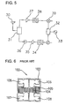
- a general constitution of a surface acoustic wave apparatus as an example of electronic component apparatuses adapted to use a facedown mounting method using the aforementioned metallic bump, will be explained with reference to Figs. 6 to 8.
- Fig. 6 is a plan view of a surface acoustic wave element used for a surface acoustic wave apparatus.
- Fig. 7 is a sectional view of a surface acoustic wave apparatus in which this surface acoustic wave element is put in a package.
- Fig. 8 is an enlarged sectional view of a connecting portion of an electrode pad part of the surface acoustic wave element and a pattern electrode of the package with a metallic bump disposed therebetween.
- a surface acoustic wave element 102 is composed of a piezoelectric substrate 103 and an [DT 104, a reflector 105, an input electrode 106, an output electrode 107, and ground electrodes 108, which are formed of a conductive thin film containing A1 as a primary component. on the piezoelectric substrate 103.
- the IDT 104 and the reflector 105 are element electrodes for functions of the surface acoustic wave element 102
- the input electrode 106, the output electrode 107, and the ground electrodes 108 are electrode pads to be connected to a circuit substrate and a package.
- a surface acoustic wave element 102 is mounted facedown in a package 109.
- Theoutput electrode 107 and an electrode pattern 109a disposed on the package 109, and one ground electrode 108 and an electrode pattern 109b disposed on the package 109 are connected, respectively, by Au bumps 110.
- the input electrode 106 and the other ground electrode 108 are also connected to electrode patterns provided on the package 109 via Au bumps 110.
- the reference numerals 109c and 109d indicate external electrodes connected to electrode patterns 109a and 109b, respectively.
- Each electrode 104 to 108 disposed on the piezoelectric substrate 103 is formed by producing a metallic thin film about 0.1 ⁇ m to 0.2 ⁇ m in film thickness containing Al as a primary component using a vapor deposition method or a sputtering method on the piezoelectric substrate 103, and thereafter, patterning the thin film into a predetermined shape by photolithography and etching. Since each electrode is formed at the same time using vapor deposition, etc., as described above, film thicknesses of the input electrode 106, the output electrode 107, and the ground electrodes 108 being electrode pads are determined based on a film thickness of the IDT 104.
- the film thickness of the IDT 104 has to be about 0.1 ⁇ m to 0.2 ⁇ m
- the thicknesses of the electrode pads cannot exceed the aforementioned thickness of the IDT. Therefore, when the Au bump is formed directly on the aforementioned electrode pad about 0.1 ⁇ m to 0.2 ⁇ m in thickness, and the surface acoustic wave element 102 is mounted facedown on the package 109 with the Au bump therebetween, the strength of electrode pad parts is decreased so that, for example, electrode pads peel off, and therefore sufficient connection strength cannot be achieved.
- an upper electrode 111 about 1 ⁇ m in thickness made of a metal containing Al as a primary component was further provided using vapor deposition or sputtering on the ground electrode 108 being the electrode pad formed on the piezoelectric substrate 103, and therefore the thickness of the electrode pad was secured so as to realize sufficient connection strength.
- upper electrodes 111 are also formed on the input electrode 106 and the output electrode 107 in a manner similar to that of the ground electrode 108. Since the input electrode 106, the output electrode 107, and the ground electrodes 108 are composed of a metal containing Al as a primary component, surfaces of these electrodes are likely to be oxidized.
- the intermediate electrodes for example, made of Ti, having superior connection strength with Al, were provided between the upper electrodes and the input electrode, the output electrode, and the ground electrodes so as to increase connection strength, the stress was concentrated not at the connection part of the intermediate electrode, but at the piezoelectric substrate. Consequently, there was a problem in that cracks and fractures occurred in the piezoelectric substrate. It was found that the cracks and fractures in the piezoelectric substrate would cause problems, for example, damage to elements, decrease in connection strength, and disconnection of electrical continuity, so that functions of a surface acoustic wave apparatus were degraded.
- the cracks and fractures in the piezoelectric substrate are caused by the various stresses applied to the piezoelectric substrate during the face-down mounting process, a sealing process, and other related processes. It has been confirmed by the inventor of the present invention that, even when various parameters used in the face-down mounting process such as power and the duration of application of ultrasonic waves, a heating temperature, or an amount of a pressing weight and parameters used in the sealing process such as a heating temperature, a heating duration, dimensions of electrodes are optimized so as to reduce the occurrence of the cracks and fractures, it is impossible to prevent the cracks in the piezoelectric substrate and ensure the sufficient connection strength between the electrodes and the bumps.
- preferred embodiments of the present invention provide an electronic element, wherein in the case in which an electronic element is facing an electrode pattern provided on a package or a circuit substrate with an Au bump therebetween, and pressure is applied while an ultrasonic wave or heat is applied so as to connect the electrode pattern and the Au bump, even when a large stress is applied to a portion of the electronic element attached to the Au bump, problems such as cracks and fractures in an element substrate do not occur.
- An electronic element includes a substrate, an electrode disposed on the substrate, an electrode pad connected to the electrode, an upper electrode disposed on the electrode pad and connected to a metallic bump, and an intermediate electrode disposed between the electrode pad and the upper electrode.
- the intermediate electrode preferably includes a single layer made of a metal other than a metal constituting the electrode pad or the upper electrode, and a thickness of the intermediate electrode is preferably greater than about 50 nm.
- the intermediate electrode may be composed of a plurality of layers made of a metal other than a metal constituting the electrode pad or the upper electrode, and a total thickness of the plurality of layers preferably exceeds approximately 50 nm.
- the thickness of the aforementioned intermediate electrode or the sum of the plurality of layers is preferably about 100 nm or more.
- the metal constituting the aforementioned electrode pad or the aforementioned upper electrode is Al, and the aforementioned intermediate electrode is preferably one metal selected from the group consisting of Ni, Cr, NiCr, and Ti.
- the aforementioned metallic bump is preferably made of Au or a metallic material containing Au as a primary component.
- At least one layer of the substrate electrode may be provided between the electrode pad and the element substrate.
- the aforementioned facedown mounting is performed using an ultrasonic wave.
- the electronic element is preferably a surface acoustic wave element, and the electronic element is preferably mounted in a package via a facedown mounting method.
- the cracks and fractures that occurred in the substrate with conventional methods do not occur because of the differentiation of the material of the intermediate electrode from the material of the electrode pad or the upper electrode, which disperses the stress applied to the piezoelectric substrate at boundaries with each layer of the electrode pad. the intermediate electrode, and the upper electrode during the mounting.
- the cracking in the piezoelectric substrate is prevented from occurring by not only differentiating the material of the intermediate electrode from the material of the electrode pad or the upper electrode.
- a thickness thereof preferably exceeds about 50 nm, preferably to be about 100 nm or more, so as to prevent the cracking in the piezoelectric substrate from occurring.
- the intermediate electrode disperses into the electrode pad or the upper electrode, and therefore, the layer of the intermediate electrode disappears, and the electrode pad, the intermediate electrode, and the upper electrode are made to be one electrode pad so that the stress cannot be dispersed at the boundaries of layers.
- the thickness of each metallic layer may be decreased. Not all of the layers are, however, considered to disappear by this increase in the number of layers, so that the stress can be dispersed at the boundaries of the layers. Accordingly, the total thickness of the metallic layers other than the electrode pad and the upper electrode is larger than a thickness corresponding to about 50 nm, and preferably, the total thickness of metallic layers other than the electrode pad and the upper electrode is larger than about 100 nm.
- the electronic element or the surface acoustic wave element may be mounted in a package container using the aforementioned mounting method, and the package container may be sealed airtight with a cap to produce an electronic component or a surface acoustic wave apparatus.
- the adhesive strength between the metallic bump and the electrode pad is sufficient, and cracking and fracturing do not occur in the element substrate, damage to electronic elements and a decrease in connection strength can be prevented. Therefore, it is useful for improving yields of electronic elements and electronic part apparatuses, for decreasing failure rates, for improving reliabilities, and other characteristics thereof.
- Fig. 1 is a plan view of a surface acoustic wave element according to a preferred embodiment of the present invention.
- Fig. 2 is a sectional view of a surface acoustic wave apparatus according to a first preferred embodiment of the present invention.
- Fig. 3 is an enlarged sectional view of a mounting portion joined via a metallic bump on a package of a surface acoustic wave apparatus according to a second preferred embodiment of the present invention.
- Fig. 4 is an enlarged sectional view of a mounting portion joined via a metallic bump on a package of a surface acoustic wave apparatus according to a third preferred embodiment of the present invention.
- Fig. 5 is a block diagram showing in part a communications apparatus according to fourth preferred embodiment of the present invention.
- Fig. 6 is a plan view of a conventional surface acoustic wave element.
- Fig. 7 is a sectional view of a conventional surface acoustic wave apparatus.
- Fig. 8 is an enlarged sectional view of a mounting portion joined via a bump electrode on a package of the conventional surface acoustic wave element.
- Fig. 1 is a plan view of a surface acoustic wave element used for a surface acoustic wave apparatus
- Fig. 2 is a sectional view of a surface acoustic wave apparatus in which a surface acoustic wave element is put in a package.
- a surface acoustic wave element 2 preferably includes a piezoelectric substrate 3 preferably made of lithium tantalite or other suitable material, IDTs and reflectors of two longitudinally coupled double mode surface acoustic wave filters 4 and 5 defined by a thin film of about 100 nm to about 400 nm in thickness made of Al on the piezoelectric substrate 3, and upper electrodes 11 disposed on an input electrode 6, an output electrode 7, and ground electrodes 8 with intermediate electrodes therebetween.
- the IDTs and reflectors of the two longitudinally coupled double mode surface acoustic wave filters 4 and 5 are element electrodes for functions of the surface acoustic wave element 2, and the input electrode 6, the output electrode 7, and the ground electrodes 8 are electrode pads for connecting to a circuit substrate and a package.
- a surface acoustic wave apparatus 1 is the one in which a surface acoustic wave element 2 is mounted facedown in a package 9, preferably made of a ceramics material.
- An upper electrode 11 having a thickness of about 1 ⁇ m, made of Al and located on the output electrode 7 with an intermediate electrode 12 made of a NiCr alloy film of about 200 nm in thickness therebetween and an electrode pattern 9a made of Au and provided on the package 9 are connected with an Au bump 10 therebetween.
- the input electrode 6 and another ground electrode 8 are similarly connected to an electrode pattern disposed on the package 9 with an Au bump 10 therebetween.
- Reference numerals 9c and 9d indicate external electrodes made of Au, and these electrodes are connected to the electrode patterns 9a and 9b, respectively.
- a cap of the package 9 may be made of the same ceramics material as the part for containing the surface acoustic wave element 2, or may be a metallic board.
- an Al thin film of about 100 nm to about 400 nm in thickness is formed on the piezoelectric substrate 3 using, for example, a vapor deposition method or a sputtering method, and thereafter, the thin film is patterned in a predetermined shape using photolithography and etching so as to form the IDTs and reflectors of longitudinally coupled double mode surface acoustic wave filters 4 and 5, and to form the input electrode 6, the output electrode 7, and the ground electrodes 8 defining electrode pads.
- the intermediate electrodes 12 about 200 nm in thickness made of NiCr are formed on the input electrode 6, the output electrode 7, and the ground electrodes 8 by, for example, vapor deposition using a lift-off method, or other suitable method, and sputtering, and thereafter.
- the upper electrodes 11 about 1 ⁇ m in thickness made of A1 are formed on the intermediate electrodes 12 by vapor deposition, sputtering, or other suitable process, in the same manner as described above.
- the Au bumps 10 are formed on the thus formed upper electrodes 11 preferably using a ball bonding method. Specifically, a ball formed at the tip of an Au wire is adhered by pressing on the upper electrode 11 while an ultrasonic wave is being applied, and thereafter, the Au wire is cut off from the ball part to form the Au bump 10.
- the surface of the surface acoustic wave element formed by way of the aforementioned processes is arranged to face the electrode patterns 9a and 9b formed on the package 9 with the Au bumps 10 therebetween, and the element is pressed while an ultrasonic wave and heat are being applied so as to connect them. Then, the package 9 is sealed airtight with the cap so as to complete the surface acoustic wave apparatus 1.
- Table 1 shows results of examinations of layer thicknesses of the intermediate electrodes 12 and rates of occurrence of cracks occurring in the piezoelectric substrate.
- conditions of the examined surface acoustic wave apparatuses were that electrode pads and element electrodes were about 350 nm of A1 electrodes, intermediate electrodes were NiCr electrodes, upper electrodes were about 1 ⁇ m of A1 electrodes, and the other specifications were the same as those of the surface acoustic wave apparatus 1 shown in Fig. 2.
- the number examined was less than 150 when the layer thicknesses of intermediate electrodes were about 400 nm and about 500 nm, because items that were determined to be defective before the examinations of cracks were rejected.
- Thickness of Intermediate electrode [nm] Number of cracks occurring / Number of Examination Rate of cracks occurrence 10 7/200 3.5% 50 6/200 3.0% 100 0/200 0.0% 150 0/150 0.0% 200 0/200 0.0% 250 0/150 0.0% 300 0/150 0.0% 400 0/149 0.0% 500 0/148 0.0%
- the layer thickness of the intermediate electrode preferably exceeds about 50 nm as shown in Table 1.
- the layer thickness of the intermediate electrode when the layer thickness of the intermediate electrode is about 100 nm or more, the cracking in the piezoelectric substrate can be prevented from occurring. Although it is clearly shown in Table 1 that the rate of defective items decreases with increasing layer thickness of the intermediate electrode, since more cost and time are required with increasing layer thickness, it is considered best that the layer thickness of the intermediate electrode be about 200 nm.
- FIG. 3 is an enlarged sectional view of a mounting part via a metallic bump on a package of a surface acoustic wave apparatus according to the second preferred embodiment.
- the same elements as in the first preferred embodiment according to the present invention as shown in Figs. 1 and 2 are indicated by the same reference numerals as in the first preferred embodiment. and detail explanations thereof are omitted.
- the intermediate electrode according to the first preferred embodiment is a monolayer electrode of about 200 nm in thickness made of NiCr
- the intermediate electrode according to the present preferred embodiment is a multilayer electrode including a plurality of layers.
- an intermediate electrode 12 between a ground electrode 8 disposed on a piezoelectric substrate 3 and an upper electrode 11 has a three-layered structure. That is, the intermediate electrode preferably includes a NiCr layer 12a of about 50 nm in thickness, an A1 layer 12b of about 1 ⁇ m in thickness, and a Ti layer 12c of about 50 nm in thickness, in order from the piezoelectric substrate 3 side.
- the other ground electrodes, an input electrode, and an output electrode have constitutions similar to the constitution as shown in Fig. 3.
- the thickness of the intermediate electrode 12 is preferably about 1100 nm.
- the cracking in the piezoelectric substrate 3 cannot be prevented from occurring even when the thickness of the entirety of the intermediate electrode 12 becomes about 100 nm or more as a result of increasing the layer thickness, in the intermediate electrode 12, made of the same kind of metal as the ground electrode 8 and the upper electrode 11 being electrode pads. Therefore, the total thickness of the NiCr layer 12a and the Ti layer 12c preferably exceeds about 50 nm, and is preferably specifically about 100 nm in this preferred embodiment.
- the dispersion of the stress at boundaries of layers is reliably achieved, so that the cracking and the fracturing in the piezoelectric substrate are prevented from occurring.
- FIG. 4 is an enlarged sectional view of a mounting portion joined via a metallic bump on a package of a surface acoustic wave apparatus according to the third preferred embodiment.
- the same elements as in the first preferred embodiment according to the present invention as shown in Figs. 1 and 2, and in the second preferred embodiment according to the present invention as shown in Fig. 3, are indicated by the same reference numerals as in the first and second preferred embodiments, and detailed explanations thereof are omitted.
- a substrate electrode 13 is disposed between a ground electrode 8 defining an electrode pad and a piezoelectric substrate 3, and the Al layer 12b in the intermediate electrode 12 in the second preferred embodiment is not provided.
- an intermediate electrode 12 between the ground electrode 8 disposed on the piezoelectric substrate 3 and an upper electrode 11 has a two-layered structure. That is. the intermediate electrode preferably includes a NiCr layer 12a of about 50 nm in thickness and a Ti layer 12c of about 50 nm in thickness, in order from the piezoelectric substrate 3 side.
- the dispersion of the stress at boundaries of layers is made possible. so that the cracking and the fracturing in the piezoelectric substrate can be prevented from occurring.
- the substrate electrode 13 of about 10 nm in thickness made of Ti is disposed between the piezoelectric substrate 3 and the ground electrode 8 defining an electrode pad.
- an adhesive strength of the piezoelectric substrate 3 and the ground electrode 8 defining an electrode pad is greatly improved, and electrical characteristics of a surface acoustic wave element are greatly improved.
- the other ground electrodes, an input electrode, and an output electrode have constitutions similar to the constitution as shown in Fig. 4.
- piezoelectric substrate made of lithium tantalate as an element substrate.
- insulating substrates provided with a lithium niobate or zinc oxide film and piezoelectric substrates, such as quartz and langasite, and other suitable substrates may be used and can exhibit similar effects.
- the element electrodes and the electrode pads, and the upper electrodes are preferably defined by Al electrodes.
- alloying metallic materials such as an alloy made of Al and 5% of added Cu, and Au.
- Other suitable materials may also be used.
- the Au bump formed using the ball bonding as an example.
- a bump forming method by plating may be used.
- the bump itself may be a metallic bump such as an A1 bump.
- the Au bump formed using the ball bonding is preferable.
- the substrate electrode made of Ti as an example.
- Cu, Cr, or other suitable materials may be used as the substrate electrode, and the thickness thereof is not limited to about 10 nm as long as an adhesive strength of the piezoelectric substrate and the electrode pad can be improved.
- the ultrasonic wave and heat are preferably applied at the same time for the facedown mounting.
- a method applying heat only or an ultrasonic wave only may be used.
- the constitution of various preferred embodiments of the present invention is suitable for a facedown mounting using a method applying at least an ultrasonic wave.
- a communications apparatus preferably includes an antenna 30, a duplexer 31 connected to the antenna 30, a transmitting circuit and a receiving circuit both of which are connected to the duplexer 30.
- the transmitting circuit includes an inter-stage filter 34 to filter a signal that is generated at a oscillator 33 and divided by a divider 32, a power amplifier to amplify a transmitting signal and an isolator 36 to prevent a receiving signal from transmitting to a transmitting circuit.
- the receiving circuit includes a low-noise amplifier 37 to amplify a receiving signal from the antenna 30 and an inter-stage filter 38 to filter the receiving signal.
- An IF signal is output from a mixer 39 by mixing the receiving signal and the local signal.
Landscapes
- Surface Acoustic Wave Elements And Circuit Networks Thereof (AREA)
- Wire Bonding (AREA)
Applications Claiming Priority (4)
| Application Number | Priority Date | Filing Date | Title |
|---|---|---|---|
| JP2000049445 | 2000-02-25 | ||
| JP2000049445 | 2000-02-25 | ||
| JP2001013514A JP2001313305A (ja) | 2000-02-25 | 2001-01-22 | 電子部品素子、電子部品装置および通信機装置 |
| JP2001013514 | 2001-01-22 |
Publications (2)
| Publication Number | Publication Date |
|---|---|
| EP1128423A2 true EP1128423A2 (de) | 2001-08-29 |
| EP1128423A3 EP1128423A3 (de) | 2004-03-10 |
Family
ID=26586108
Family Applications (1)
| Application Number | Title | Priority Date | Filing Date |
|---|---|---|---|
| EP01400488A Withdrawn EP1128423A3 (de) | 2000-02-25 | 2001-02-23 | Flip-Chip montierte elektronische Vorrichtung mit Mehrlagen-Elektroden |
Country Status (5)
| Country | Link |
|---|---|
| US (1) | US20040108560A1 (de) |
| EP (1) | EP1128423A3 (de) |
| JP (1) | JP2001313305A (de) |
| KR (1) | KR20010085606A (de) |
| CN (1) | CN1319948A (de) |
Families Citing this family (9)
| Publication number | Priority date | Publication date | Assignee | Title |
|---|---|---|---|---|
| EP1313214B1 (de) * | 2001-11-16 | 2020-02-26 | SnapTrack, Inc. | Verpackungssubstrat, integrierte Schaltungvorrichtung, deren jeweilige Herstellungsverfahren und akustische Oberflächenwellenvorrichtung |
| JP2003318212A (ja) * | 2002-04-26 | 2003-11-07 | Murata Mfg Co Ltd | 蒸着リフトオフによるバンプ形成に用いるレジストパターンおよびその形成方法、バンプおよびその形成方法、ならびに弾性表面波素子およびその製造方法 |
| US7141909B2 (en) * | 2003-06-17 | 2006-11-28 | Murata Manufacturing Co., Ltd. | Surface acoustic wave device |
| JP2006202938A (ja) * | 2005-01-20 | 2006-08-03 | Kojiro Kobayashi | 半導体装置及びその製造方法 |
| US20070069367A1 (en) * | 2005-09-28 | 2007-03-29 | Honeywell International Inc. | Reduced stress on SAW die with surrounding support structures |
| JP4770643B2 (ja) | 2005-10-12 | 2011-09-14 | エプソントヨコム株式会社 | 圧電デバイス及び、その製造方法 |
| JP4674555B2 (ja) * | 2006-02-20 | 2011-04-20 | エプソントヨコム株式会社 | 弾性表面波素子及び通信装置 |
| WO2013147741A1 (en) * | 2012-03-26 | 2013-10-03 | Empire Technology Development Llc | Color tunable substrate |
| JP2014013795A (ja) * | 2012-07-03 | 2014-01-23 | Seiko Epson Corp | ベース基板、電子デバイスおよび電子機器 |
Family Cites Families (7)
| Publication number | Priority date | Publication date | Assignee | Title |
|---|---|---|---|---|
| KR910006967B1 (ko) * | 1987-11-18 | 1991-09-14 | 가시오 게이상기 가부시기가이샤 | 반도체 장치의 범프 전극 구조 및 그 형성 방법 |
| US5156997A (en) * | 1991-02-11 | 1992-10-20 | Microelectronics And Computer Technology Corporation | Method of making semiconductor bonding bumps using metal cluster ion deposition |
| DE69223868T2 (de) * | 1991-07-17 | 1998-09-03 | Denso Corp | Verfahren zur Herstellung von Elektroden eines Halbleiterbauelements |
| US5587336A (en) * | 1994-12-09 | 1996-12-24 | Vlsi Technology | Bump formation on yielded semiconductor dies |
| JP3275775B2 (ja) * | 1997-05-16 | 2002-04-22 | 株式会社村田製作所 | 弾性表面波装置 |
| JP3795644B2 (ja) * | 1997-09-25 | 2006-07-12 | 東芝電子エンジニアリング株式会社 | 接合方法 |
| JPH11234082A (ja) * | 1998-02-13 | 1999-08-27 | Toko Inc | 表面弾性波装置 |
-
2001
- 2001-01-22 JP JP2001013514A patent/JP2001313305A/ja active Pending
- 2001-02-21 US US09/789,363 patent/US20040108560A1/en not_active Abandoned
- 2001-02-23 EP EP01400488A patent/EP1128423A3/de not_active Withdrawn
- 2001-02-26 KR KR1020010009671A patent/KR20010085606A/ko not_active Ceased
- 2001-02-26 CN CN01108873A patent/CN1319948A/zh active Pending
Also Published As
| Publication number | Publication date |
|---|---|
| CN1319948A (zh) | 2001-10-31 |
| JP2001313305A (ja) | 2001-11-09 |
| EP1128423A3 (de) | 2004-03-10 |
| US20040108560A1 (en) | 2004-06-10 |
| KR20010085606A (ko) | 2001-09-07 |
Similar Documents
| Publication | Publication Date | Title |
|---|---|---|
| US6552475B2 (en) | Surface acoustic wave device | |
| US10250222B2 (en) | Electronic device | |
| EP0637871B1 (de) | Schaltungsbaustein mit akustischer Oberflächenwellenanordnung | |
| US7112913B2 (en) | Surface acoustic wave apparatus and manufacturing method therefor | |
| US6731046B2 (en) | Surface acoustic wave element and manufacturing method of the same | |
| US10665566B2 (en) | Surface acoustic wave resonator having ring-shaped metal sealing configuration | |
| US6437439B1 (en) | Electronic component | |
| US7274129B2 (en) | Surface acoustic wave device and method of fabricating the same | |
| JP3351402B2 (ja) | 電子素子、弾性表面波素子、それらの実装方法、電子部品または弾性表面波装置の製造方法、および、弾性表面波装置 | |
| US6911762B2 (en) | Surface acoustic wave element, surface acoustic wave device using the same, and method for manufacturing surface acoustic wave element and surface acoustic wave device | |
| EP1128423A2 (de) | Flip-Chip montierte elektronische Vorrichtung mit Mehrlagen-Elektroden | |
| JP4066952B2 (ja) | 電子部品素子、電子部品、及び通信機 | |
| JP3716123B2 (ja) | 弾性表面波装置 | |
| JP2004129193A (ja) | 弾性表面波装置 | |
| JP2003051677A (ja) | 多層基板への電子部品実装方法および多層基板に電子部品が実装された電子部品装置 | |
| JP2000353934A (ja) | 弾性表面波装置 | |
| JP2003086625A (ja) | 電子部品素子、電子部品装置 | |
| JP2004254012A (ja) | 圧電振動体の支持構造 | |
| JPH08213873A (ja) | 弾性表面波素子デバイス | |
| JP2022028566A (ja) | 弾性波デバイス | |
| JP2002246870A (ja) | 弾性表面波装置とその製造装置 | |
| GB2381976A (en) | Electrode pad construction and connection for surface acoustic wave apparatus | |
| JPH09116373A (ja) | Sawチップ及びこれを用いたsawデバイスの製造方法 | |
| JP2002344278A (ja) | 圧電共振子 |
Legal Events
| Date | Code | Title | Description |
|---|---|---|---|
| PUAI | Public reference made under article 153(3) epc to a published international application that has entered the european phase |
Free format text: ORIGINAL CODE: 0009012 |
|
| 17P | Request for examination filed |
Effective date: 20010302 |
|
| AK | Designated contracting states |
Kind code of ref document: A2 Designated state(s): AT BE CH CY DE DK ES FI FR GB GR IE IT LI LU MC NL PT SE TR |
|
| AX | Request for extension of the european patent |
Free format text: AL;LT;LV;MK;RO;SI |
|
| PUAL | Search report despatched |
Free format text: ORIGINAL CODE: 0009013 |
|
| AK | Designated contracting states |
Kind code of ref document: A3 Designated state(s): AT BE CH CY DE DK ES FI FR GB GR IE IT LI LU MC NL PT SE TR |
|
| AX | Request for extension of the european patent |
Extension state: AL LT LV MK RO SI |
|
| AKX | Designation fees paid |
Designated state(s): DE FR GB |
|
| STAA | Information on the status of an ep patent application or granted ep patent |
Free format text: STATUS: THE APPLICATION IS DEEMED TO BE WITHDRAWN |
|
| 18D | Application deemed to be withdrawn |
Effective date: 20040911 |