EP1128440A2 - Profil eines Halbleiter-Übergangs und Verfahren zur Herstellung - Google Patents
Profil eines Halbleiter-Übergangs und Verfahren zur Herstellung Download PDFInfo
- Publication number
- EP1128440A2 EP1128440A2 EP01301158A EP01301158A EP1128440A2 EP 1128440 A2 EP1128440 A2 EP 1128440A2 EP 01301158 A EP01301158 A EP 01301158A EP 01301158 A EP01301158 A EP 01301158A EP 1128440 A2 EP1128440 A2 EP 1128440A2
- Authority
- EP
- European Patent Office
- Prior art keywords
- slice
- conductivity type
- substrate
- junction
- regions
- Prior art date
- Legal status (The legal status is an assumption and is not a legal conclusion. Google has not performed a legal analysis and makes no representation as to the accuracy of the status listed.)
- Withdrawn
Links
Images


Classifications
-
- H—ELECTRICITY
- H10—SEMICONDUCTOR DEVICES; ELECTRIC SOLID-STATE DEVICES NOT OTHERWISE PROVIDED FOR
- H10D—INORGANIC ELECTRIC SEMICONDUCTOR DEVICES
- H10D62/00—Semiconductor bodies, or regions thereof, of devices having potential barriers
- H10D62/10—Shapes, relative sizes or dispositions of the regions of the semiconductor bodies; Shapes of the semiconductor bodies
- H10D62/102—Constructional design considerations for preventing surface leakage or controlling electric field concentration
- H10D62/103—Constructional design considerations for preventing surface leakage or controlling electric field concentration for increasing or controlling the breakdown voltage of reverse-biased devices
- H10D62/104—Constructional design considerations for preventing surface leakage or controlling electric field concentration for increasing or controlling the breakdown voltage of reverse-biased devices having particular shapes of the bodies at or near reverse-biased junctions, e.g. having bevels or moats
Definitions
- the shallow negative bevel technique is often applied to one junction of a device while applying a positive bevel to a junction on the opposite face.
- This is a very suitable combination for devices consisting of a silicon slice soldered to a backing plate of a refractory metal, e.g. tungsten or molybdenum, the positive bevel being applied to the face soldered to the backing plate.
- a refractory metal e.g. tungsten or molybdenum
- a method of producing a semiconductor junction profile comprising providing a planar slice of semiconductor substrate material of a first conductivity type provided at one face with a first region of a second conductivity type having a higher dopant concentration than that of the substrate and at the opposite face a second region of said second conductivity type, having a higher dopant concentration than that of the substrate, the method comprising removing from part of each of said faces by abrasion a depth of material which increases gradually as the outer edge is approached so that the junction between each of said regions and the substrate is exposed along a path following the shape of the perimeter of the slice but so that the removal of material ceases at a distance outwardly beyond the exposure of the junction to leave a rim of the original planar faces of the slice at its perimeter.
- the slice may be a disc and the material of the slice may be silicon.
- the edge of the slice may be rounded in section.
- Said first and second regions of said second conductivity type may be formed by the diffusion of a dopant of said second conductivity type into the faces of the substrate so as to over-dope the original first conductivity type and form a junction therewith at a predetermined depth.
- Said first and second regions of said second conductivity type may extend around the outer edge of the slice to form a surface region which is broken only where each of said junctions is exposed.
- the gradual increase in depth of the removal of material may constitute an angle of less than 7° relative to the plane of the junction thereby exposed, for example in the range from 2° to 5°, such as about 3°.
- the substrate material may be of n-type conductivity and the surface regions of p-type conductivity.
- the present invention also comprises a slice according to the invention with the addition of further semiconductor regions and ohmically connected electrodes so as to form an operable electrical device.
- FIG. 1 there is represented a slice 1 of silicon consisting of three regions.
- a central substrate region 2 of high resistivity n-type silicon is sandwiched between two outer surface regions 3a, 3b each of lower resistivity p-type material.
- the surface regions 3a, 3b will have been formed by in-diffusion of a p-type dopant as is well known in the art, resulting in a gaussian or complementary error function concentration profile extending inwards of the surface to the junction with the substrate region 2. It is a general rule for the optimisation of the shallow negative bevel technique that the diffused-in concentration profile should be well graded rather than abrupt.
- the lines between the outer regions 3a, 3b and the central region 2 represent the respective semiconductor junctions 4a, 4b.
- the thinnest part of the slice 1 is the part beyond the emergence at the bevelled surfaces 5a, 5b of the junctions 4a, 4b.
- Space charge regions 6a, 6b build up around whichever of the respective junctions is in reverse bias mode.
- the extents of the space charge regions 6a, 6b may overlap in the planar part of the slice, but for clarity they are shown here as they would behave at a moderate reverse bias for each junction.
- these space charge regions extend mainly into the high resistivity substrate region 2 of the silicon disc.
- the space charge region is constrained by the effect of the bevel angle 7, typically about 3°, to extend instead mainly into the respective diffused surface region 3a or 3b.
- a range of bevel angles in the range from 2° to 7° may be employed, smaller angles producing greater penetration of the space charge into the p-type surface region and being correspondingly appropriate to higher voltage designs.
- the effect of the space charge at each surface extending into the p-type surface region 3a or 3b, rather than into the substrate region 2, is that the edge part 2e of the substrate region lying beyond the extent of either of space charge regions 6a, 6b is never depleted of carriers and correspondingly remains always conductive.
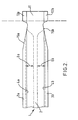
- FIG. 2 wherein numerals previously used in Figure 1 retain the same meaning, there is shown a slice (at least 100mm in diameter) similar in all respects to Figure 1 except for the cessation of bevelled surfaces 15a, 15b before reaching the rim 11 of the slice 1 which thereby retains its original thickness. It can be seen that the extent of the space charge regions 6a, 6b associated with the respective junctions 4a, 4b is unaffected by the presence of the rim of full thickness silicon even though this now includes outer parts 13a, 13b of the diffused surface regions 3a, 3b that were removed in the formation of the prior art shape shown in Figure 1. The advantages secured by the structure of Figure 2 will now be described.
- the normal method of forming the shape of Figure 1 is carefully and gently to abrade the silicon surface using a tool of complementary profile.
- this might be a section of a spherical bowl of accurately defined curvature so that the angle of the bevel where it exposes the junction 4a or 4b is at the desired value.
- the sine of the angle produced in this way is equal to the ratio of the radius R of the exposure line of the junction 4a or 4b to the radius of curvature of the bowl.
- the bowl may contain an abrasive slurry or its surface may be impregnated with an abrasive material, e.g. diamond.
- an abrasive material e.g. diamond.
- the amount of reactive force that can safely be applied in the abrading procedure is limited by a combination of the mechanical strength of silicon and the extent to which its opposite face is effectively supported.
- the slice may be supported over the whole of the original opposite surface of region 3b or at least part of it facing the area of abrasion of surface 5a. This is not a difficult task as the face requiring support is, at this stage, flat.
- Effectively supporting the second face to be bevelled, the first face already having been shaped poses a greater problem as the shape of the first formed bevel requires to be accurately followed. It is important not to apply a cantilevered flexing force to the silicon, particularly while lapping or grinding it, as this can very easily cause a stress fracture nucleated at a micro-scratch.
- the bevelled surface 15a is ground to shape using an abrasive wheel while supporting the still flat surface of the opposite side.
- the process leaves the outer rim 11 with its original thickness.
- the slice is now turned over and the operation repeated on the second face while supporting the first face on each side of the area to be ground away, i.e. inwardly towards its centre and outwardly at the rim.
- the area of the silicon being worked on has now only to bridge between two areas of support resulting in compressive rather than tensile stresses in the surface area being abraded. The stress in the silicon material is thus more easily contained within safe limits.
- FIG 3 there is shown the outer edge region of a slice prepared essentially as in Figure 2.
- Numerals used previously again have the same meaning as in Figures 1 and 2.
- the silicon slice has its outer edge surface 22 rounded so that external sharp corners are avoided.
- the edge may be rounded in the original slice before its several processing stages resulting in the outer parts of the diffused surface regions 13a, 13b being joined by a continuation around the edge of the slice as shown in the Figure, or it may be ground to shape shortly before the bevelling step.
- the advantage provided by the edge rounding is a much enhanced resistance to mechanical damage such as chipping. This not only protects the slice itself but also avoids the generation of splinters of silicon which are detrimental to the general cleanliness of the work environment.
- the preservation of the rim thickness in the bevel method disclosed serves also to preserve the shape of the edge rounding which, if applied to the prior art technique, would be partially removed by the bevel extending to the edge of the slice and thereby become less effective.
- the embodiments describe those features essential to the voltage blocking ability typical of a thyristor or gate turn-off device without reference to some of the other necessary features of these devices such as gate electrodes and additional emitter junctions.
- the invention is applicable generally to semiconductor devices of the floating type requiring two opposed blocking junctions as will be apparent to those skilled in the art, and is especially useful for slices at least 100mm in diameter.
Landscapes
- Thyristors (AREA)
- Mechanical Treatment Of Semiconductor (AREA)
- Element Separation (AREA)
Applications Claiming Priority (2)
| Application Number | Priority Date | Filing Date | Title |
|---|---|---|---|
| GB0004050A GB2359415A (en) | 2000-02-21 | 2000-02-21 | Profiling of semiconductor wafer to prevent edge breakdown |
| GB0004050 | 2000-02-21 |
Publications (2)
| Publication Number | Publication Date |
|---|---|
| EP1128440A2 true EP1128440A2 (de) | 2001-08-29 |
| EP1128440A3 EP1128440A3 (de) | 2003-10-22 |
Family
ID=9886101
Family Applications (1)
| Application Number | Title | Priority Date | Filing Date |
|---|---|---|---|
| EP01301158A Withdrawn EP1128440A3 (de) | 2000-02-21 | 2001-02-09 | Profil eines Halbleiter-Übergangs und Verfahren zur Herstellung |
Country Status (4)
| Country | Link |
|---|---|
| US (1) | US20010022389A1 (de) |
| EP (1) | EP1128440A3 (de) |
| JP (1) | JP2001284200A (de) |
| GB (1) | GB2359415A (de) |
Family Cites Families (8)
| Publication number | Priority date | Publication date | Assignee | Title |
|---|---|---|---|---|
| GB1052447A (de) * | 1962-09-15 | |||
| GB1068199A (en) * | 1963-11-26 | 1967-05-10 | Int Rectifier Corp | High voltage semiconductor device |
| FR2468207A1 (fr) * | 1979-10-23 | 1981-04-30 | Thomson Csf | Structure de sillon de separation dans une plaquette semiconductrice et son procede de fabrication |
| JPS607178A (ja) * | 1983-06-27 | 1985-01-14 | Toshiba Corp | 半導体装置 |
| DE3331298A1 (de) * | 1983-08-31 | 1985-03-14 | Brown, Boveri & Cie Ag, 6800 Mannheim | Leistungsthyristor auf einem substrat |
| DE3422051C2 (de) * | 1984-06-14 | 1986-06-26 | Brown, Boveri & Cie Ag, 6800 Mannheim | Silizium-Halbleiterbauelement mit ätztechnisch hergestellter Randkontur und Verfahren zur Herstellung dieses Bauelements |
| US4579760A (en) * | 1985-01-08 | 1986-04-01 | International Business Machines Corporation | Wafer shape and method of making same |
| JPH0624200B2 (ja) * | 1989-04-28 | 1994-03-30 | 信越半導体株式会社 | 半導体デバイス用基板の加工方法 |
-
2000
- 2000-02-21 GB GB0004050A patent/GB2359415A/en not_active Withdrawn
-
2001
- 2001-02-09 EP EP01301158A patent/EP1128440A3/de not_active Withdrawn
- 2001-02-13 US US09/782,618 patent/US20010022389A1/en not_active Abandoned
- 2001-02-21 JP JP2001045336A patent/JP2001284200A/ja active Pending
Also Published As
| Publication number | Publication date |
|---|---|
| GB2359415A (en) | 2001-08-22 |
| JP2001284200A (ja) | 2001-10-12 |
| EP1128440A3 (de) | 2003-10-22 |
| GB0004050D0 (en) | 2000-04-12 |
| US20010022389A1 (en) | 2001-09-20 |
Similar Documents
| Publication | Publication Date | Title |
|---|---|---|
| EP0393951B1 (de) | Halbleitendes Siliciumwafer und sein Herstellungsverfahren | |
| EP0396326B1 (de) | Verfahren zur Behandlung eines Substrats für Halbleiter-Bauelemente | |
| US5314844A (en) | Method for dicing a semiconductor wafer | |
| US5177908A (en) | Polishing pad | |
| CN100355025C (zh) | 可拆除基片或可拆除结构及其生产方法 | |
| US20080135975A1 (en) | Semiconductor wafer, method of manufacturing the same and semiconductor device | |
| US4254590A (en) | Method for the production of a disk-shaped silicon semiconductor component with negative beveling | |
| US8796820B2 (en) | Semiconductor wafer and semiconductor device wafer | |
| US6113721A (en) | Method of bonding a semiconductor wafer | |
| KR20210122816A (ko) | 인화인듐 기판 및 인화인듐 기판의 제조 방법 | |
| JP3239884B2 (ja) | 半導体基板の製造方法 | |
| EP1128440A2 (de) | Profil eines Halbleiter-Übergangs und Verfahren zur Herstellung | |
| EP1004399A2 (de) | Flachschliff- und Hochglanzpolierverfahren | |
| US7179720B2 (en) | Pre-fabrication scribing | |
| CN108555700A (zh) | 一种碳化硅晶片的抛光工艺 | |
| CN109571232B (zh) | 晶圆研磨方法及其研磨系统 | |
| US7816233B2 (en) | Method of manufacturing composite wafer structure | |
| JP3964029B2 (ja) | 半導体基板の製造方法 | |
| US5766973A (en) | Method for manufacturing a semiconductor arrangement by introducing crystal disorder structures and varying diffusion rates | |
| EP4207249A1 (de) | Indiumphosphidsubstrat, verfahren zur herstellung eines indiumphosphidsubstrats und epitaktischer halbleiterwafer | |
| JPH01271178A (ja) | 半導体ウエハ用ダイシングブレード | |
| US9337037B2 (en) | Method for obtaining a heterogeneous substrate for the production of semiconductors | |
| US20250201566A1 (en) | Method for manufacturing semiconductor apparatus and semiconductor apparatus | |
| JP4151155B2 (ja) | ノッチ付化合物半導体ウェハの製造方法 | |
| EP4170700A1 (de) | Indiumphosphidsubstrat |
Legal Events
| Date | Code | Title | Description |
|---|---|---|---|
| PUAI | Public reference made under article 153(3) epc to a published international application that has entered the european phase |
Free format text: ORIGINAL CODE: 0009012 |
|
| AK | Designated contracting states |
Kind code of ref document: A2 Designated state(s): AT BE CH CY DE DK ES FI FR GB GR IE IT LI LU MC NL PT SE TR |
|
| AX | Request for extension of the european patent |
Free format text: AL;LT;LV;MK;RO;SI |
|
| PUAL | Search report despatched |
Free format text: ORIGINAL CODE: 0009013 |
|
| AK | Designated contracting states |
Kind code of ref document: A3 Designated state(s): AT BE CH CY DE DK ES FI FR GB GR IE IT LI LU MC NL PT SE TR |
|
| AX | Request for extension of the european patent |
Extension state: AL LT LV MK RO SI |
|
| AKX | Designation fees paid | ||
| REG | Reference to a national code |
Ref country code: DE Ref legal event code: 8566 |
|
| STAA | Information on the status of an ep patent application or granted ep patent |
Free format text: STATUS: THE APPLICATION IS DEEMED TO BE WITHDRAWN |
|
| 18D | Application deemed to be withdrawn |
Effective date: 20040423 |