EP1134794A1 - Couche mince et composant a semi-conducteur - Google Patents
Couche mince et composant a semi-conducteur Download PDFInfo
- Publication number
- EP1134794A1 EP1134794A1 EP99931499A EP99931499A EP1134794A1 EP 1134794 A1 EP1134794 A1 EP 1134794A1 EP 99931499 A EP99931499 A EP 99931499A EP 99931499 A EP99931499 A EP 99931499A EP 1134794 A1 EP1134794 A1 EP 1134794A1
- Authority
- EP
- European Patent Office
- Prior art keywords
- thin film
- film
- hydrogen
- less
- silicon
- Prior art date
- Legal status (The legal status is an assumption and is not a legal conclusion. Google has not performed a legal analysis and makes no representation as to the accuracy of the status listed.)
- Withdrawn
Links
Images
Classifications
-
- H—ELECTRICITY
- H10—SEMICONDUCTOR DEVICES; ELECTRIC SOLID-STATE DEVICES NOT OTHERWISE PROVIDED FOR
- H10F—INORGANIC SEMICONDUCTOR DEVICES SENSITIVE TO INFRARED RADIATION, LIGHT, ELECTROMAGNETIC RADIATION OF SHORTER WAVELENGTH OR CORPUSCULAR RADIATION
- H10F71/00—Manufacture or treatment of devices covered by this subclass
- H10F71/121—The active layers comprising only Group IV materials
-
- C—CHEMISTRY; METALLURGY
- C23—COATING METALLIC MATERIAL; COATING MATERIAL WITH METALLIC MATERIAL; CHEMICAL SURFACE TREATMENT; DIFFUSION TREATMENT OF METALLIC MATERIAL; COATING BY VACUUM EVAPORATION, BY SPUTTERING, BY ION IMPLANTATION OR BY CHEMICAL VAPOUR DEPOSITION, IN GENERAL; INHIBITING CORROSION OF METALLIC MATERIAL OR INCRUSTATION IN GENERAL
- C23C—COATING METALLIC MATERIAL; COATING MATERIAL WITH METALLIC MATERIAL; SURFACE TREATMENT OF METALLIC MATERIAL BY DIFFUSION INTO THE SURFACE, BY CHEMICAL CONVERSION OR SUBSTITUTION; COATING BY VACUUM EVAPORATION, BY SPUTTERING, BY ION IMPLANTATION OR BY CHEMICAL VAPOUR DEPOSITION, IN GENERAL
- C23C16/00—Chemical coating by decomposition of gaseous compounds, without leaving reaction products of surface material in the coating, i.e. chemical vapour deposition [CVD] processes
- C23C16/22—Chemical coating by decomposition of gaseous compounds, without leaving reaction products of surface material in the coating, i.e. chemical vapour deposition [CVD] processes characterised by the deposition of inorganic material, other than metallic material
- C23C16/24—Deposition of silicon only
-
- C—CHEMISTRY; METALLURGY
- C30—CRYSTAL GROWTH
- C30B—SINGLE-CRYSTAL GROWTH; UNIDIRECTIONAL SOLIDIFICATION OF EUTECTIC MATERIAL OR UNIDIRECTIONAL DEMIXING OF EUTECTOID MATERIAL; REFINING BY ZONE-MELTING OF MATERIAL; PRODUCTION OF A HOMOGENEOUS POLYCRYSTALLINE MATERIAL WITH DEFINED STRUCTURE; SINGLE CRYSTALS OR HOMOGENEOUS POLYCRYSTALLINE MATERIAL WITH DEFINED STRUCTURE; AFTER-TREATMENT OF SINGLE CRYSTALS OR A HOMOGENEOUS POLYCRYSTALLINE MATERIAL WITH DEFINED STRUCTURE; APPARATUS THEREFOR
- C30B25/00—Single-crystal growth by chemical reaction of reactive gases, e.g. chemical vapour-deposition growth
- C30B25/02—Epitaxial-layer growth
-
- C—CHEMISTRY; METALLURGY
- C30—CRYSTAL GROWTH
- C30B—SINGLE-CRYSTAL GROWTH; UNIDIRECTIONAL SOLIDIFICATION OF EUTECTIC MATERIAL OR UNIDIRECTIONAL DEMIXING OF EUTECTOID MATERIAL; REFINING BY ZONE-MELTING OF MATERIAL; PRODUCTION OF A HOMOGENEOUS POLYCRYSTALLINE MATERIAL WITH DEFINED STRUCTURE; SINGLE CRYSTALS OR HOMOGENEOUS POLYCRYSTALLINE MATERIAL WITH DEFINED STRUCTURE; AFTER-TREATMENT OF SINGLE CRYSTALS OR A HOMOGENEOUS POLYCRYSTALLINE MATERIAL WITH DEFINED STRUCTURE; APPARATUS THEREFOR
- C30B29/00—Single crystals or homogeneous polycrystalline material with defined structure characterised by the material or by their shape
- C30B29/02—Elements
- C30B29/06—Silicon
-
- C—CHEMISTRY; METALLURGY
- C30—CRYSTAL GROWTH
- C30B—SINGLE-CRYSTAL GROWTH; UNIDIRECTIONAL SOLIDIFICATION OF EUTECTIC MATERIAL OR UNIDIRECTIONAL DEMIXING OF EUTECTOID MATERIAL; REFINING BY ZONE-MELTING OF MATERIAL; PRODUCTION OF A HOMOGENEOUS POLYCRYSTALLINE MATERIAL WITH DEFINED STRUCTURE; SINGLE CRYSTALS OR HOMOGENEOUS POLYCRYSTALLINE MATERIAL WITH DEFINED STRUCTURE; AFTER-TREATMENT OF SINGLE CRYSTALS OR A HOMOGENEOUS POLYCRYSTALLINE MATERIAL WITH DEFINED STRUCTURE; APPARATUS THEREFOR
- C30B29/00—Single crystals or homogeneous polycrystalline material with defined structure characterised by the material or by their shape
- C30B29/02—Elements
- C30B29/08—Germanium
-
- H—ELECTRICITY
- H10—SEMICONDUCTOR DEVICES; ELECTRIC SOLID-STATE DEVICES NOT OTHERWISE PROVIDED FOR
- H10F—INORGANIC SEMICONDUCTOR DEVICES SENSITIVE TO INFRARED RADIATION, LIGHT, ELECTROMAGNETIC RADIATION OF SHORTER WAVELENGTH OR CORPUSCULAR RADIATION
- H10F10/00—Individual photovoltaic cells, e.g. solar cells
- H10F10/10—Individual photovoltaic cells, e.g. solar cells having potential barriers
- H10F10/17—Photovoltaic cells having only PIN junction potential barriers
-
- H—ELECTRICITY
- H10—SEMICONDUCTOR DEVICES; ELECTRIC SOLID-STATE DEVICES NOT OTHERWISE PROVIDED FOR
- H10P—GENERIC PROCESSES OR APPARATUS FOR THE MANUFACTURE OR TREATMENT OF DEVICES COVERED BY CLASS H10
- H10P14/00—Formation of materials, e.g. in the shape of layers or pillars
- H10P14/20—Formation of materials, e.g. in the shape of layers or pillars of semiconductor materials
- H10P14/24—Formation of materials, e.g. in the shape of layers or pillars of semiconductor materials using chemical vapour deposition [CVD]
-
- H—ELECTRICITY
- H10—SEMICONDUCTOR DEVICES; ELECTRIC SOLID-STATE DEVICES NOT OTHERWISE PROVIDED FOR
- H10P—GENERIC PROCESSES OR APPARATUS FOR THE MANUFACTURE OR TREATMENT OF DEVICES COVERED BY CLASS H10
- H10P14/00—Formation of materials, e.g. in the shape of layers or pillars
- H10P14/20—Formation of materials, e.g. in the shape of layers or pillars of semiconductor materials
- H10P14/29—Formation of materials, e.g. in the shape of layers or pillars of semiconductor materials characterised by the substrates
- H10P14/2901—Materials
- H10P14/2922—Materials being non-crystalline insulating materials, e.g. glass or polymers
-
- H—ELECTRICITY
- H10—SEMICONDUCTOR DEVICES; ELECTRIC SOLID-STATE DEVICES NOT OTHERWISE PROVIDED FOR
- H10P—GENERIC PROCESSES OR APPARATUS FOR THE MANUFACTURE OR TREATMENT OF DEVICES COVERED BY CLASS H10
- H10P14/00—Formation of materials, e.g. in the shape of layers or pillars
- H10P14/20—Formation of materials, e.g. in the shape of layers or pillars of semiconductor materials
- H10P14/29—Formation of materials, e.g. in the shape of layers or pillars of semiconductor materials characterised by the substrates
- H10P14/2901—Materials
- H10P14/2923—Materials being conductive materials, e.g. metallic silicides
-
- H—ELECTRICITY
- H10—SEMICONDUCTOR DEVICES; ELECTRIC SOLID-STATE DEVICES NOT OTHERWISE PROVIDED FOR
- H10P—GENERIC PROCESSES OR APPARATUS FOR THE MANUFACTURE OR TREATMENT OF DEVICES COVERED BY CLASS H10
- H10P14/00—Formation of materials, e.g. in the shape of layers or pillars
- H10P14/20—Formation of materials, e.g. in the shape of layers or pillars of semiconductor materials
- H10P14/32—Formation of materials, e.g. in the shape of layers or pillars of semiconductor materials characterised by intermediate layers between substrates and deposited layers
- H10P14/3202—Materials thereof
- H10P14/3204—Materials thereof being Group IVA semiconducting materials
- H10P14/3211—Silicon, silicon germanium or germanium
-
- H—ELECTRICITY
- H10—SEMICONDUCTOR DEVICES; ELECTRIC SOLID-STATE DEVICES NOT OTHERWISE PROVIDED FOR
- H10P—GENERIC PROCESSES OR APPARATUS FOR THE MANUFACTURE OR TREATMENT OF DEVICES COVERED BY CLASS H10
- H10P14/00—Formation of materials, e.g. in the shape of layers or pillars
- H10P14/20—Formation of materials, e.g. in the shape of layers or pillars of semiconductor materials
- H10P14/34—Deposited materials, e.g. layers
- H10P14/3402—Deposited materials, e.g. layers characterised by the chemical composition
- H10P14/3404—Deposited materials, e.g. layers characterised by the chemical composition being Group IVA materials
- H10P14/3408—Silicon carbide
-
- H—ELECTRICITY
- H10—SEMICONDUCTOR DEVICES; ELECTRIC SOLID-STATE DEVICES NOT OTHERWISE PROVIDED FOR
- H10P—GENERIC PROCESSES OR APPARATUS FOR THE MANUFACTURE OR TREATMENT OF DEVICES COVERED BY CLASS H10
- H10P14/00—Formation of materials, e.g. in the shape of layers or pillars
- H10P14/20—Formation of materials, e.g. in the shape of layers or pillars of semiconductor materials
- H10P14/34—Deposited materials, e.g. layers
- H10P14/3402—Deposited materials, e.g. layers characterised by the chemical composition
- H10P14/3404—Deposited materials, e.g. layers characterised by the chemical composition being Group IVA materials
- H10P14/3411—Silicon, silicon germanium or germanium
-
- H—ELECTRICITY
- H10—SEMICONDUCTOR DEVICES; ELECTRIC SOLID-STATE DEVICES NOT OTHERWISE PROVIDED FOR
- H10P—GENERIC PROCESSES OR APPARATUS FOR THE MANUFACTURE OR TREATMENT OF DEVICES COVERED BY CLASS H10
- H10P14/00—Formation of materials, e.g. in the shape of layers or pillars
- H10P14/20—Formation of materials, e.g. in the shape of layers or pillars of semiconductor materials
- H10P14/34—Deposited materials, e.g. layers
- H10P14/3438—Doping during depositing
- H10P14/3441—Conductivity type
- H10P14/3442—N-type
-
- H—ELECTRICITY
- H10—SEMICONDUCTOR DEVICES; ELECTRIC SOLID-STATE DEVICES NOT OTHERWISE PROVIDED FOR
- H10P—GENERIC PROCESSES OR APPARATUS FOR THE MANUFACTURE OR TREATMENT OF DEVICES COVERED BY CLASS H10
- H10P14/00—Formation of materials, e.g. in the shape of layers or pillars
- H10P14/20—Formation of materials, e.g. in the shape of layers or pillars of semiconductor materials
- H10P14/34—Deposited materials, e.g. layers
- H10P14/3438—Doping during depositing
- H10P14/3441—Conductivity type
- H10P14/3444—P-type
-
- H—ELECTRICITY
- H10—SEMICONDUCTOR DEVICES; ELECTRIC SOLID-STATE DEVICES NOT OTHERWISE PROVIDED FOR
- H10D—INORGANIC ELECTRIC SEMICONDUCTOR DEVICES
- H10D30/00—Field-effect transistors [FET]
- H10D30/01—Manufacture or treatment
- H10D30/021—Manufacture or treatment of FETs having insulated gates [IGFET]
- H10D30/031—Manufacture or treatment of FETs having insulated gates [IGFET] of thin-film transistors [TFT]
- H10D30/0321—Manufacture or treatment of FETs having insulated gates [IGFET] of thin-film transistors [TFT] comprising silicon, e.g. amorphous silicon or polysilicon
-
- Y—GENERAL TAGGING OF NEW TECHNOLOGICAL DEVELOPMENTS; GENERAL TAGGING OF CROSS-SECTIONAL TECHNOLOGIES SPANNING OVER SEVERAL SECTIONS OF THE IPC; TECHNICAL SUBJECTS COVERED BY FORMER USPC CROSS-REFERENCE ART COLLECTIONS [XRACs] AND DIGESTS
- Y02—TECHNOLOGIES OR APPLICATIONS FOR MITIGATION OR ADAPTATION AGAINST CLIMATE CHANGE
- Y02E—REDUCTION OF GREENHOUSE GAS [GHG] EMISSIONS, RELATED TO ENERGY GENERATION, TRANSMISSION OR DISTRIBUTION
- Y02E10/00—Energy generation through renewable energy sources
- Y02E10/50—Photovoltaic [PV] energy
-
- Y—GENERAL TAGGING OF NEW TECHNOLOGICAL DEVELOPMENTS; GENERAL TAGGING OF CROSS-SECTIONAL TECHNOLOGIES SPANNING OVER SEVERAL SECTIONS OF THE IPC; TECHNICAL SUBJECTS COVERED BY FORMER USPC CROSS-REFERENCE ART COLLECTIONS [XRACs] AND DIGESTS
- Y02—TECHNOLOGIES OR APPLICATIONS FOR MITIGATION OR ADAPTATION AGAINST CLIMATE CHANGE
- Y02E—REDUCTION OF GREENHOUSE GAS [GHG] EMISSIONS, RELATED TO ENERGY GENERATION, TRANSMISSION OR DISTRIBUTION
- Y02E10/00—Energy generation through renewable energy sources
- Y02E10/50—Photovoltaic [PV] energy
- Y02E10/547—Monocrystalline silicon PV cells
-
- Y—GENERAL TAGGING OF NEW TECHNOLOGICAL DEVELOPMENTS; GENERAL TAGGING OF CROSS-SECTIONAL TECHNOLOGIES SPANNING OVER SEVERAL SECTIONS OF THE IPC; TECHNICAL SUBJECTS COVERED BY FORMER USPC CROSS-REFERENCE ART COLLECTIONS [XRACs] AND DIGESTS
- Y02—TECHNOLOGIES OR APPLICATIONS FOR MITIGATION OR ADAPTATION AGAINST CLIMATE CHANGE
- Y02E—REDUCTION OF GREENHOUSE GAS [GHG] EMISSIONS, RELATED TO ENERGY GENERATION, TRANSMISSION OR DISTRIBUTION
- Y02E10/00—Energy generation through renewable energy sources
- Y02E10/50—Photovoltaic [PV] energy
- Y02E10/548—Amorphous silicon PV cells
-
- Y—GENERAL TAGGING OF NEW TECHNOLOGICAL DEVELOPMENTS; GENERAL TAGGING OF CROSS-SECTIONAL TECHNOLOGIES SPANNING OVER SEVERAL SECTIONS OF THE IPC; TECHNICAL SUBJECTS COVERED BY FORMER USPC CROSS-REFERENCE ART COLLECTIONS [XRACs] AND DIGESTS
- Y02—TECHNOLOGIES OR APPLICATIONS FOR MITIGATION OR ADAPTATION AGAINST CLIMATE CHANGE
- Y02P—CLIMATE CHANGE MITIGATION TECHNOLOGIES IN THE PRODUCTION OR PROCESSING OF GOODS
- Y02P70/00—Climate change mitigation technologies in the production process for final industrial or consumer products
- Y02P70/50—Manufacturing or production processes characterised by the final manufactured product
-
- Y—GENERAL TAGGING OF NEW TECHNOLOGICAL DEVELOPMENTS; GENERAL TAGGING OF CROSS-SECTIONAL TECHNOLOGIES SPANNING OVER SEVERAL SECTIONS OF THE IPC; TECHNICAL SUBJECTS COVERED BY FORMER USPC CROSS-REFERENCE ART COLLECTIONS [XRACs] AND DIGESTS
- Y10—TECHNICAL SUBJECTS COVERED BY FORMER USPC
- Y10T—TECHNICAL SUBJECTS COVERED BY FORMER US CLASSIFICATION
- Y10T428/00—Stock material or miscellaneous articles
- Y10T428/12—All metal or with adjacent metals
- Y10T428/12493—Composite; i.e., plural, adjacent, spatially distinct metal components [e.g., layers, joint, etc.]
- Y10T428/12528—Semiconductor component
-
- Y—GENERAL TAGGING OF NEW TECHNOLOGICAL DEVELOPMENTS; GENERAL TAGGING OF CROSS-SECTIONAL TECHNOLOGIES SPANNING OVER SEVERAL SECTIONS OF THE IPC; TECHNICAL SUBJECTS COVERED BY FORMER USPC CROSS-REFERENCE ART COLLECTIONS [XRACs] AND DIGESTS
- Y10—TECHNICAL SUBJECTS COVERED BY FORMER USPC
- Y10T—TECHNICAL SUBJECTS COVERED BY FORMER US CLASSIFICATION
- Y10T428/00—Stock material or miscellaneous articles
- Y10T428/12—All metal or with adjacent metals
- Y10T428/12493—Composite; i.e., plural, adjacent, spatially distinct metal components [e.g., layers, joint, etc.]
- Y10T428/12674—Ge- or Si-base component
-
- Y—GENERAL TAGGING OF NEW TECHNOLOGICAL DEVELOPMENTS; GENERAL TAGGING OF CROSS-SECTIONAL TECHNOLOGIES SPANNING OVER SEVERAL SECTIONS OF THE IPC; TECHNICAL SUBJECTS COVERED BY FORMER USPC CROSS-REFERENCE ART COLLECTIONS [XRACs] AND DIGESTS
- Y10—TECHNICAL SUBJECTS COVERED BY FORMER USPC
- Y10T—TECHNICAL SUBJECTS COVERED BY FORMER US CLASSIFICATION
- Y10T428/00—Stock material or miscellaneous articles
- Y10T428/24—Structurally defined web or sheet [e.g., overall dimension, etc.]
- Y10T428/24802—Discontinuous or differential coating, impregnation or bond [e.g., artwork, printing, retouched photograph, etc.]
- Y10T428/24917—Discontinuous or differential coating, impregnation or bond [e.g., artwork, printing, retouched photograph, etc.] including metal layer
-
- Y—GENERAL TAGGING OF NEW TECHNOLOGICAL DEVELOPMENTS; GENERAL TAGGING OF CROSS-SECTIONAL TECHNOLOGIES SPANNING OVER SEVERAL SECTIONS OF THE IPC; TECHNICAL SUBJECTS COVERED BY FORMER USPC CROSS-REFERENCE ART COLLECTIONS [XRACs] AND DIGESTS
- Y10—TECHNICAL SUBJECTS COVERED BY FORMER USPC
- Y10T—TECHNICAL SUBJECTS COVERED BY FORMER US CLASSIFICATION
- Y10T428/00—Stock material or miscellaneous articles
- Y10T428/26—Web or sheet containing structurally defined element or component, the element or component having a specified physical dimension
- Y10T428/263—Coating layer not in excess of 5 mils thick or equivalent
- Y10T428/264—Up to 3 mils
- Y10T428/265—1 mil or less
Definitions
- the present invention relates to an improvement in the quality of a semiconductor thin film and an improvement in the performance of a semiconductor thin film device, and is widely applicable to functional thin film devices such as thin film transistors and photovoltaic devices.
- amorphous Group IV semiconductors are remarkably improved by terminating unjoined bonds (dangling bonds) of, for example, an amorphous semiconductor or polycrystalline semiconductor, with hydrogen atoms to inactivate them.
- unjoined bonds dangling bonds
- hydrogen atoms For introducing hydrogen atoms, techniques of implanting activated hydrogen gas into a semiconductor material that does not contain hydrogen or that has insufficient termination with hydrogen are mainly used. Specific examples include an ion implanting method and a plasma hydrogen doping method.
- these methods introduce hydrogen particles of high energy and thus cause damages to the semiconductor bulk material, or require a high-temperature process at a certain temperature level or higher to incorporate hydrogen atoms efficiently. Further, they require both steps of forming a semiconductor material and of hydrogenating it, thus increasing the number of processing steps.
- an object of the present invention is to improve the quality of a hydrogenated semiconductor thin film formed by a low-temperature plasma CVD method by controlling the state of hydrogen atoms in the thin film, as well as to enhance the performance of the semiconductor thin film device.
- the present invention provides a semiconductor thin film which is deposited by using a chemical vapor deposition method at an underlying layer temperature of 400°C or less, and contains, as main component elements, a Group IV atom and hydrogen atom, wherein a temperature dependency of an amount of release of hydrogen atoms within the film when the film is heated from room temperature exhibits a profile having a peak of the hydrogen releasing amount at 370°C or higher and 410°C or less, and a half-value width of the peak is 30°C or less, more preferably 20°C or less.
- the present invention provides a thin film device comprising a semiconductor unit portion including a semiconductor thin film of the present invention and an electrode portion including a electrically conductive thin film, wherein these portions are formed on the same substrate.
- Semiconductor thin films to which an embodiment of the present invention is applied, can be formed by a method described below.
- the chemical vapor deposition which is a method of forming a semiconductor thin film
- a generally and widely used parallel plate-type RF plasma CVD method can be employed. It may be of a type in which a high frequency power of an RF to VHF band at the frequency of 150 MHz or less can also be used.
- the film forming temperature is set at 400°C or less for a reason that hydrogen atoms contained in the film will not be released while forming the film but remain in sufficient amount, and for another reason that an inexpensive substrate can be used.
- a gas of a hydrogenated Group IV element is used as the main component of the raw material gas introduced into a reaction chamber. In the case of silicon, for example, monosilane, disilane or dichlorsilane can be used.
- a raw material for carbon methane can be used, and as a raw material for germanium, germane or the like is used.
- a dilution gas is introduced into the reaction chamber.
- hydrogen gas is mainly used, and further an inert gas such as noble gas, preferably helium, neon, argon or the like may be used. It is preferable that the flow rate of the dilution gas with respect to that of the raw material gas should be 20 times or more, and an optimal dilution amount is determined based on the combination with other film forming conditions such as the temperature of the underlying substrate, discharge power and the pressure within the reaction chamber.
- the semiconductor thin film having the Group IV element as a main component contains a relatively large amount of hydrogen atoms which serves to terminate and inactivate defects at crystal grain boundaries or within a grain, since it is formed at a low temperature.
- the distribution of the bonding state between the Group IV atoms and hydrogen atoms can be estimated from the dependency of the hydrogen atom releasing amount on the increase in the temperature while the formed film is being gradually heated from room temperature. The relationship between the released hydrogen amount and temperature corresponds to the bonding energy between the Group IV atom and hydrogen atom within the film.
- the semiconductor thin film of the present invention is characterized by its profile having one peak within a range of 370°C or more and 410°C or less, with a half-value width of the peak of 30°C or less, more preferably, 20°C or less, in that diagram.
- the thin film device to which an embodiment of the present invention is applied, has a semiconductor unit portion including a semiconductor thin film, as described above, containing Group IV atom and hydrogen atom as its main components.
- the thickness of the semiconductor thin film should preferably be in a range of 0.1 ⁇ m or more and 20 ⁇ m or less. If the thickness of the film is less than this range, the film is insufficient in terms of volume to achieve the device performance, whereas if it exceeds the range, the production cost for such a semiconductor thin film becomes high, which impairs the merit of the thin film device.
- the thin film device has an electrode portion including an electrically conductive thin film, in addition to the above-described semiconductor unit portion, which are laminated on the same substrate.
- the thin film device may further include an insulating thin film such as a silicon oxide film or silicon nitride film laminated on the same substrate.
- the type of the thin film device examples include a MOS or MIS-type junction device such as a thin film transistor (TFT), and a p-n or p-i-n junction device such as a sensor, an imaging device and a photovoltaic device including a solar cell.
- a MOS or MIS-type junction device such as a thin film transistor (TFT)
- a p-n or p-i-n junction device such as a sensor
- an imaging device an imaging device
- a photovoltaic device including a solar cell examples of the type of the thin film device.
- a metal such as stainless, an organic film or an inexpensive glass having a low melting point, or the like is used.
- a thin film layer formed of one or more of the item (A) and (B) below is formed by, for example, a vapor deposition method or sputtering method.
- a photovoltaic unit of an n-i-p or p-i-n junction is formed.
- all of the layers which constitute the photovoltaic unit are deposited by the plasma CVD method under a condition that the temperature of the substrate is 400°C or less.
- a generally and widely used parallel plate-type RF plasma CVD method is employed. Use may also be made of the plasma CVD method using a high frequency power of an RF to VHF band at a frequency of 150 MHz or less.
- a one conductivity type layer is deposited.
- an n-type silicon-based thin film to which phosphorus atoms, which are conductivity type-determining impurity atoms, have been doped, or a p-type silicon-based thin film to which boron atoms have been doped, or the like can be used.
- the impurity atom for example, nitrogen or the like may be used in an n-type layer.
- the one conductivity type layer it is possible to use an alloy material such as amorphous silicon carbide or amorphous silicon germanium, in addition to amorphous silicon, or also possible to use polycrystalline silicon, microcrystalline silicon partially containing crystalline one, or an alloy metallic material thereof.
- the percent crystallinity and the carrier concentration due to the conductivity-determining impurity atom are controlled by irradiating a pulse laser beam after the deposition of the one conductivity type layer
- a hydrogenated silicon-based thin film which is the semiconductor thin film of the present invention, is deposited.
- a non-doped intrinsic thin film silicon or a silicon-based thin film material of a weak p-type or weak n-type, which contains a very small amount of impurity, and has a sufficient photoelectric conversion function should be used.
- the present invention is not limited to these, and alloy materials such as silicon carbide and silicon germanium may be used.
- the thickness of the photoelectric conversion layer is 0.1 to 20 ⁇ m which provides a necessary and sufficient thickness as the silicon-based thin film photoelectric conversion layer.
- a silicon-based thin film of a conductivity type opposite to the one conductivity type described above is deposited.
- the opposite conductivity type layer for example, a p-type silicon-based thin film to which boron atoms, which are conductivity type determining impurity atomd, have been doped, or an n-type silicon-based thin film to which phosphorus atoms have been doped, or the like is used.
- the impurity atom for example, aluminum or the like may be used in the p-type layer.
- an alloy material such as amorphous silicon carbide or amorphous silicon germanium, in addition to amorphous silicon, or also possible to use polycrystalline silicon, microcrystalline silicon containing crystalline materials partially, or an alloy metallic material.
- a transparent conductive oxide film made of at least one layer of material selected from the group consisting of ITO, SnO 2 and ZnO is formed by, for example, a vapor deposition method or sputtering method.
- a comb-shaped metal electrode made of at least one material selected from the group consisting of Al, Ag, Au, Cu and Pt, or an alloy layer thereof is formed on the oxide film, providing a grid electrode.
- thin film silicon photovoltaic devices which serve as photovoltaic devices according to some examples of the present invention, and comparative examples, will be described below.
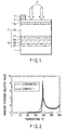
- a Ti film 101, Ag film 102 and a ZnO film 103 were formed to thicknesses of 50 nm, 300 nm and 100 nm, respectively, by the sputtering method to provide a rear electrode 10.
- a phosphorus-doped n-type silicon layer 111, a non-doped thin film silicon photoelectric conversion layer 112, and a p-type silicon layer 113 were formed to thicknesses of 20 nm, 2.5 micrometers and 10 nm, respectively, each by the RF plasma CVD method to provide an n-i-p junction silicon photovoltaic unit 11.
- a transparent conductive film (ITO) having a thickness of 80 nm was formed as an upper electrode and a comb-shaped Ag electrode 3 for outputting an electric current was formed.
- the hydrogenated silicon film which provides the thin film silicon photoelectric conversion layer 112
- the reaction gas was obtained by mixing silane and hydrogen at a flow rate ratio of 1 : 90, and the pressure within the reaction chamber was set at 5.0 Torr. Further, the discharge power density was set at 100 mW/cm 2 and the film forming temperature was set at 30°C.
- the hydrogenated silicon film formed under these film forming conditions was subjected to a secondary ion mass spectrometry, and the hydrogen atom content within the film was measured to be 2.5 atomic %.
- the output properties of this thin film silicon photovoltaic device when an incident light 4 having an AM of 1.5 and a light intensity of 100 mW/cm 2 was used were: a open circuit voltage of 0.520 volts, a short-circuit current density of 27.4 mA/cm 2 , a fill factor of 75.1% and a photoelectric conversion efficiency of 10.7%.
- a thin film silicon photovoltaic device was formed on a glass substrate.
- the film forming conditions and the device structure were the same as in Example 1 described above, except for the film forming conditions for a photoelectric conversion layer 112.
- the hydrogenated silicon film which provides the thin film silicon photoelectric conversion layer 112
- the other film forming conditions were the same as in Example 1 except that the reaction gas was obtained by mixing silane and hydrogen at a flow rate ratio of 1 : 150.
- the hydrogenated silicon film formed was subjected to a secondary ion mass spectrometry, and the hydrogen atom content within the film was measured to be 2.8 atomic %.
- the output properties of this thin film silicon photovoltaic device when an incident light 4 having an AM of 1.5 and a light intensity of 100 mW/cm 2 was used were: a open circuit voltage of 0.402 volts, a short-circuit current density of 27.7 mA/cm 2 , a fill factor of 73.1% and a photoelectric conversion efficiency of 8.1%.
- the process in which hydrogen within the hydrogenated silicon film was released with an increase in the heating temperature of the film was analyzed.
- a sample was placed in a mass spectrometer for a gas released with an increasing temperature.
- the starting temperature was set at room temperature (about 20°C), and the sample was heated to a finishing temperature of 600°C at a rate of 10°C per minute.
- the gas released from the film the relative value of the amount of released H 2 molecule having a mass number of 2 was monitored.
- Example 2 With regard to the photovoltaic devices described in Example 1 and comparative Example 1 above, the sample in each case at the point where the photovoltaic unit 11 has been formed was subjected to the analysis of the increasing temperature dependency of the released hydrogen amount, and the results were presented in FIG. 2.
- the thickness of each of the n- and p-type conductivity type layers was very small as compared to that of the photoelectric conversion layer, and therefore it was determined that most of the released hydrogen observed was from the non-doped hydrogenated silicon film which is the photoelectric conversion layer.
- Each case indicates a profile having one peak at a temperature near 388°C, and it is observed that the released hydrogen was concentrated near this temperature.
- Example 1 stronger release of hydrogen was observed within a narrower temperature range. From the estimation of the half-width value obtained by taking an interval between the temperatures at which the hydrogen releasing amount is a half of the peak value, it was 11°C in Example 1, whereas 70°C in Comparative Example 1. As already mentioned above, there was no significant difference between the both cases in terms of physical properties including the absolute value of the total hydrogen amount contained in the film; however the performance as the photovoltaic device is clearly higher in Example 1. The relationship between the released hydrogen and temperature corresponds to the bonding energy between silicon and hydrogen atoms within the film (note that it is considered that most of the bonding is for the passivation of the crystal grain boundaries).
- Hydrogenated silicon films were formed under the conditions presented in TABLE 1, and thin film silicon photovoltaic devices were formed on glass substrates as in Example 1 and Comparative Example 1, respectively. In each case, the hydrogen content in the film and the half-value width of a peak appearing near 390°C in a temperature profile of the hydrogen releasing amount obtained by the analysis of release due to heating are presented as well.
- the film forming conditions and device structures of the other layers than those of the hydrogenated silicon film which gives rise to the thin film silicon photoelectric conversion layer 112 are the same as those of Example 1.
- the results of the output properties of the photovoltaic device were as presented in TABLE 2. Voc (volts) Jsc (mA/cm 2 ) F.F. (%) Eff.
- Example 2 0.471 27.2 74.9 9.6
- Example 3 0.488 27.0 75.9 10.0
- Example 4 0.529 27.0 75.2 10.7
- Example 5 0.534 26.8 76.2 10.9
- Example 6 0.540 26.5 76.1 10.6
- Comparative Example 2 0.455 27.1 73.9 9.1 Comparative Example 3 0.624 19.3 64.4 7.8 Comparative Example 4 0.712 16.8 54.8 6.6
- the parameters of the film forming conditions are various, but the films with a small half-value width in the releasing hydrogen amount temperature profile were obtained by appropriately selecting a combination of these parameters. With such combination, the conversion efficiency of each of such photovoltaic devices is high.
- the half-value width is large and therefore the conversion efficiency of the photovoltaic device in each of these cases is low. This is because, with regard to Comparative Example 2, the selected value of the gas flow rate ratio is excessively high as in the case of Comparative Example 1, and therefore the energy of the hydrogen radicals and ions is excessively applied while forming a film by the plasma CVD.
- the energy of the hydrogen radicals and ions is insufficient, and therefore the structure relaxation of the deposited film is not sufficient, but the distortion and defects are considered to be more prominent. It is further because, as compared to those of Examples of the invention, the hydrogen content within the film is relatively high, silicon-hydrogen bonds exist locally at high densities, and therefore many void-like structural portions exist.
- the hydrogenated silicon thin film of the present invention can be realized by setting such film forming conditions that can apply appropriate hydrogen radial and ion energy.
- the present invention it is possible to improve the quality of the semiconductor thin film formed at low temperature and containing, as main structural components, an Group IV element and hydrogen atoms, and therefore it becomes possible to contribute remarkably to the improvement of the performance of low-cost thin film devices including a thin film silicon-based photovoltaic device.
Landscapes
- Chemical & Material Sciences (AREA)
- Engineering & Computer Science (AREA)
- Materials Engineering (AREA)
- Metallurgy (AREA)
- Organic Chemistry (AREA)
- Crystallography & Structural Chemistry (AREA)
- Chemical Kinetics & Catalysis (AREA)
- General Chemical & Material Sciences (AREA)
- Inorganic Chemistry (AREA)
- Mechanical Engineering (AREA)
- Photovoltaic Devices (AREA)
- Chemical Vapour Deposition (AREA)
- Physical Vapour Deposition (AREA)
- Thin Film Transistor (AREA)
Applications Claiming Priority (3)
| Application Number | Priority Date | Filing Date | Title |
|---|---|---|---|
| JP20660598 | 1998-07-22 | ||
| JP20660598A JP3792903B2 (ja) | 1998-07-22 | 1998-07-22 | 半導体薄膜および薄膜デバイス |
| PCT/JP1999/003941 WO2000005754A1 (fr) | 1998-07-22 | 1999-07-22 | Couche mince et composant a semi-conducteur |
Publications (2)
| Publication Number | Publication Date |
|---|---|
| EP1134794A1 true EP1134794A1 (fr) | 2001-09-19 |
| EP1134794A4 EP1134794A4 (fr) | 2006-08-09 |
Family
ID=16526165
Family Applications (1)
| Application Number | Title | Priority Date | Filing Date |
|---|---|---|---|
| EP99931499A Withdrawn EP1134794A4 (fr) | 1998-07-22 | 1999-07-22 | Couche mince et composant a semi-conducteur |
Country Status (8)
| Country | Link |
|---|---|
| US (1) | US6617010B2 (fr) |
| EP (1) | EP1134794A4 (fr) |
| JP (1) | JP3792903B2 (fr) |
| KR (1) | KR100411897B1 (fr) |
| CN (1) | CN1149640C (fr) |
| AU (1) | AU750452B2 (fr) |
| CA (1) | CA2338314C (fr) |
| WO (1) | WO2000005754A1 (fr) |
Families Citing this family (6)
| Publication number | Priority date | Publication date | Assignee | Title |
|---|---|---|---|---|
| JP4171428B2 (ja) * | 2003-03-20 | 2008-10-22 | 三洋電機株式会社 | 光起電力装置 |
| NO20061668L (no) * | 2006-04-12 | 2007-10-15 | Renewable Energy Corp | Solcelle og fremgangsmate for fremstilling av samme |
| EP2021533A4 (fr) * | 2006-05-15 | 2010-01-06 | Arise Technologies Corp | Processus de dopage basse température pour dispositif à galette de silicium |
| CN101345270B (zh) * | 2007-07-13 | 2011-05-04 | 鸿富锦精密工业(深圳)有限公司 | 太阳能电池 |
| US8418418B2 (en) | 2009-04-29 | 2013-04-16 | 3Form, Inc. | Architectural panels with organic photovoltaic interlayers and methods of forming the same |
| CN103247718B (zh) * | 2013-04-09 | 2015-06-17 | 许昌学院 | 常温下原位控制合成硫铜银三元化合物半导体光电薄膜材料的化学方法 |
Family Cites Families (11)
| Publication number | Priority date | Publication date | Assignee | Title |
|---|---|---|---|---|
| JPH0793448B2 (ja) * | 1986-04-08 | 1995-10-09 | ティーディーケイ株式会社 | 光電変換素子 |
| JPH0212812A (ja) * | 1988-06-30 | 1990-01-17 | Tonen Corp | アモルファスシリコンカーバイド膜の光劣抑制方法 |
| JP2663580B2 (ja) * | 1988-11-22 | 1997-10-15 | 日本電気株式会社 | シリコン表面のパッシベーション方法及び装置 |
| JP2846651B2 (ja) * | 1989-03-31 | 1999-01-13 | 三洋電機株式会社 | 光起電力装置 |
| JPH0435021A (ja) * | 1990-05-31 | 1992-02-05 | Tonen Corp | 多結晶シリコン薄膜の成長方法 |
| JP2695585B2 (ja) * | 1992-12-28 | 1997-12-24 | キヤノン株式会社 | 光起電力素子及びその製造方法、並びにそれを用いた発電装置 |
| JPH0770580B2 (ja) * | 1993-03-30 | 1995-07-31 | 日本電気株式会社 | 基板表面の温度測定方法およびそれを利用した半導体成膜方法とその装置 |
| WO1995026571A1 (fr) * | 1994-03-25 | 1995-10-05 | Amoco/Enron Solar | Silicium amorphe stabilise et dispositifs contenant ce dernier |
| JPH08227167A (ja) * | 1995-02-20 | 1996-09-03 | Canon Inc | 光受容部材の製造方法および光受容部材 |
| US5719076A (en) * | 1996-04-24 | 1998-02-17 | United Solar Systems Corporation | Method for the manufacture of semiconductor devices with optimized hydrogen content |
| JP3998765B2 (ja) * | 1997-09-04 | 2007-10-31 | シャープ株式会社 | 多結晶半導体層の製造方法及び半導体装置の評価方法 |
-
1998
- 1998-07-22 JP JP20660598A patent/JP3792903B2/ja not_active Expired - Fee Related
-
1999
- 1999-07-22 WO PCT/JP1999/003941 patent/WO2000005754A1/fr not_active Ceased
- 1999-07-22 KR KR10-2001-7000772A patent/KR100411897B1/ko not_active Expired - Fee Related
- 1999-07-22 CN CNB998090050A patent/CN1149640C/zh not_active Expired - Lifetime
- 1999-07-22 CA CA002338314A patent/CA2338314C/fr not_active Expired - Fee Related
- 1999-07-22 AU AU47997/99A patent/AU750452B2/en not_active Expired
- 1999-07-22 EP EP99931499A patent/EP1134794A4/fr not_active Withdrawn
-
2001
- 2001-01-18 US US09/766,871 patent/US6617010B2/en not_active Expired - Lifetime
Also Published As
| Publication number | Publication date |
|---|---|
| JP2000040664A (ja) | 2000-02-08 |
| AU750452B2 (en) | 2002-07-18 |
| CA2338314C (fr) | 2005-03-15 |
| EP1134794A4 (fr) | 2006-08-09 |
| US20010011748A1 (en) | 2001-08-09 |
| CN1149640C (zh) | 2004-05-12 |
| KR20010070986A (ko) | 2001-07-28 |
| JP3792903B2 (ja) | 2006-07-05 |
| AU4799799A (en) | 2000-02-14 |
| WO2000005754A1 (fr) | 2000-02-03 |
| KR100411897B1 (ko) | 2003-12-18 |
| CN1310861A (zh) | 2001-08-29 |
| CA2338314A1 (fr) | 2000-02-03 |
| US6617010B2 (en) | 2003-09-09 |
Similar Documents
| Publication | Publication Date | Title |
|---|---|---|
| US6512171B2 (en) | Thin film solar cell | |
| Shah et al. | Material and solar cell research in microcrystalline silicon | |
| EP2624307B1 (fr) | Procédé de fabrication de dispositif de conversion photoélectrique | |
| AU2005200023B2 (en) | Photovoltaic device | |
| JP2951146B2 (ja) | 光起電力デバイス | |
| KR100393955B1 (ko) | 미정질 반도체 막을 포함하는 반도체 장치 | |
| US8383927B2 (en) | Stacked photovoltaic device and method of manufacturing the same | |
| US6979589B2 (en) | Silicon-based thin-film photoelectric conversion device and method of manufacturing thereof | |
| JP2006080557A (ja) | 高水素希釈低温プラズマ蒸着によって製造されるアモルファスシリコン系素子の向上せしめられた安定化特性 | |
| US6617010B2 (en) | Semiconductor thin film and thin film device | |
| JP3792376B2 (ja) | シリコン系薄膜光電変換装置 | |
| Nasuno et al. | Microcrystalline silicon thin-film solar cells prepared at low temperature | |
| EP3571723B1 (fr) | Appareil de cellule solaire et son procédé de formation pour des systèmes à jonctions simples, en tandem et à hétérojonction | |
| JP3933334B2 (ja) | シリコン系薄膜光電変換装置とその製造方法 | |
| JP2000058889A (ja) | シリコン系薄膜およびシリコン系薄膜光電変換装置 | |
| JP5123444B2 (ja) | 太陽電池の製造方法 | |
| Li | Single and multijunction silicon based thin film solar cells on a flexible substrate with absorber layers made by hot-wire CVD | |
| KR100419383B1 (ko) | 피-아이-엔(p-i-n) 비정질 실리콘 태양전지의 제조방법 | |
| Payne et al. | The effect of chlorine on dopant activation in hydrogenated amorphous silicon | |
| Muller et al. | Application of low-temperature electron cyclotron resonance CVD to silicon thin-film solar cell preparation | |
| JPH11330515A (ja) | シリコン系薄膜光電変換装置の製造方法 | |
| Agbo et al. | DEPOSITION PRESSURE AND HYDROGEN DILUTION EFFECTS ON THE SPECTRAL RESPONSE OF THIN FILM NANOCRYSTALLINE SILICON SOLAR CELLS | |
| WO2011032879A2 (fr) | Procédé de fabrication d'une photopile à base de silicium en couches minces | |
| Middya et al. | Electronic properties and device applications of hot-wire CVD polycrystalline silicon films | |
| JPH0677512A (ja) | 光起電力素子及びその製造方法、並びにそれを用いた発電システム |
Legal Events
| Date | Code | Title | Description |
|---|---|---|---|
| PUAI | Public reference made under article 153(3) epc to a published international application that has entered the european phase |
Free format text: ORIGINAL CODE: 0009012 |
|
| 17P | Request for examination filed |
Effective date: 20010220 |
|
| AK | Designated contracting states |
Kind code of ref document: A1 Designated state(s): AT BE CH CY DE DK ES FI FR GB GR IE IT LI LU MC NL PT SE |
|
| AX | Request for extension of the european patent |
Free format text: AL;LT;LV;MK;RO;SI |
|
| A4 | Supplementary search report drawn up and despatched |
Effective date: 20060712 |
|
| RIC1 | Information provided on ipc code assigned before grant |
Ipc: C30B 25/02 20060101ALN20060706BHEP Ipc: C23C 16/24 20060101ALN20060706BHEP Ipc: H01L 21/324 20060101ALI20060706BHEP Ipc: H01L 31/18 20060101ALI20060706BHEP Ipc: H01L 21/205 20060101AFI20000208BHEP |
|
| 17Q | First examination report despatched |
Effective date: 20061115 |
|
| RAP1 | Party data changed (applicant data changed or rights of an application transferred) |
Owner name: KANEKA CORPORATION |
|
| STAA | Information on the status of an ep patent application or granted ep patent |
Free format text: STATUS: THE APPLICATION IS DEEMED TO BE WITHDRAWN |
|
| 18D | Application deemed to be withdrawn |
Effective date: 20170503 |