EP1143520A2 - Zellordnungsarchitektur hoher Dichte und hoher Schnellheit - Google Patents
Zellordnungsarchitektur hoher Dichte und hoher Schnellheit Download PDFInfo
- Publication number
- EP1143520A2 EP1143520A2 EP01200089A EP01200089A EP1143520A2 EP 1143520 A2 EP1143520 A2 EP 1143520A2 EP 01200089 A EP01200089 A EP 01200089A EP 01200089 A EP01200089 A EP 01200089A EP 1143520 A2 EP1143520 A2 EP 1143520A2
- Authority
- EP
- European Patent Office
- Prior art keywords
- width
- rows
- circuit
- integrated circuit
- circuit elements
- Prior art date
- Legal status (The legal status is an assumption and is not a legal conclusion. Google has not performed a legal analysis and makes no representation as to the accuracy of the status listed.)
- Granted
Links
- 239000004065 semiconductor Substances 0.000 claims abstract description 13
- 239000000758 substrate Substances 0.000 claims abstract description 12
- 238000000034 method Methods 0.000 claims description 17
- 238000010586 diagram Methods 0.000 description 8
- 238000002955 isolation Methods 0.000 description 5
- 238000003491 array Methods 0.000 description 4
- 238000004519 manufacturing process Methods 0.000 description 3
- 230000015572 biosynthetic process Effects 0.000 description 2
- 239000000969 carrier Substances 0.000 description 1
- 230000000295 complement effect Effects 0.000 description 1
- 238000009792 diffusion process Methods 0.000 description 1
- 239000002184 metal Substances 0.000 description 1
- 229910044991 metal oxide Inorganic materials 0.000 description 1
- 150000004706 metal oxides Chemical class 0.000 description 1
Images


Classifications
-
- H—ELECTRICITY
- H10—SEMICONDUCTOR DEVICES; ELECTRIC SOLID-STATE DEVICES NOT OTHERWISE PROVIDED FOR
- H10D—INORGANIC ELECTRIC SEMICONDUCTOR DEVICES
- H10D89/00—Aspects of integrated devices not covered by groups H10D84/00 - H10D88/00
- H10D89/10—Integrated device layouts
-
- H—ELECTRICITY
- H10—SEMICONDUCTOR DEVICES; ELECTRIC SOLID-STATE DEVICES NOT OTHERWISE PROVIDED FOR
- H10D—INORGANIC ELECTRIC SEMICONDUCTOR DEVICES
- H10D84/00—Integrated devices formed in or on semiconductor substrates that comprise only semiconducting layers, e.g. on Si wafers or on GaAs-on-Si wafers
- H10D84/90—Masterslice integrated circuits
- H10D84/903—Masterslice integrated circuits comprising field effect technology
- H10D84/907—CMOS gate arrays
Definitions
- the present invention relates to the field of customized or application specific integrated circuits. More specifically, the present invention relates to an architecture for providing a customized application specific device having high functional density with high operational speed.
- Standard cell arrays are generally arranged in rows having a fixed width.
- the cells may have varying length to provide the necessary cell functionality.
- the simplest cells are inverters.
- CMOS complementary metal oxide semiconductor
- an inverter will have one N-channel and one P-channel transistor.
- routing areas for interconnecting the cells.
- Power leads may also run through the routing areas or may have designated areas overlying the cell areas.
- Standard cell arrays have been combined with powerful computerized design tools to provide high functional density with fast order turn-around time. An example of this type of device is the GS30 series provided by Texas Instruments.
- a minimum width may be six squares.
- a square is normalized unit equal to the minimum feature size that can be formed on the integrated circuit.
- Six square rows provide a very dense array.
- the maximum transistor width is about two squares (after including isolation structures between devices). A transistor this small does not provide adequate drive capacity to provide high-speed operation.
- providing wide rows for high drive transistors reduces the density of the array. The present invention solves this trade-off by providing an architecture that allows for high density and high drive transistors.
- the present invention provides an array of customizable functional cells having high density and high drive capacity.
- the present invention further provides an architecture that maximizes the width of P-channel transistors in an array of standard cells to compensate for the lower speed operation of P-type devices.
- a preferred embodiment of the present invention includes an integrated circuit having a plurality of first circuit elements, the first circuit elements having a first width. These circuit elements are arranged in a plurality of rows in a semiconductor substrate.
- the integrated circuit also includes a plurality of second circuit elements having a width of twice the width of the first circuit elements. The second circuit elements are placed in the plurality of rows and occupy the width of two of the first circuit elements.
- An alternative embodiment of the present invention includes an integrated circuit comprising a plurality of first circuit elements having a first width.
- the first circuit elements are arranged in a plurality of rows having a plurality of rows in a semiconductor substrate.
- the rows are divided into a first area of a first conductivity type and a second area of a second conductivity type.
- the first and second areas alternate in at least two adjacent rows such that the first areas of the at least two adjacent rows are positioned adjacent to each other.
- the integrated circuit includes a plurality of second circuit elements having a width of twice the first circuit elements.
- the second circuit elements positioned in the plurality of rows and occupying the width of two of the first circuit elements. At least one of the second circuit elements spans two adjacent rows.
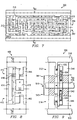
- Figure 1 is a layout diagram of a prior art cell array.
- Array 10 consists of a plurality of rows 12 for placement of circuit elements, often called standard cells.
- Figure 2 is a layout diagram of example cells as used in the prior art.
- Cell 20 is designed for high density.
- the row width for an array including cell 20 is six squares.
- Cell 20 is shown with a length of four squares. However, cells used with cell 20 may have a number of lengths.
- Cell 30 is designed for a high speed array.
- Cell 30 has a width of eight squares with a length of five squares.
- cell 30 provides the same functionality as cell 20, but the transistors in cell 30 are wider.
- transistor width is the surface dimension perpendicular to the flow of carriers in the transistor's channel region.
- a wider transistor has a greater current drive capability. Greater current drive capability allows cell 30 to operate faster than cell 20. However, an array including cell 30 will be larger for the same functionality or some functionality must be excluded if the arrays are the same size. The present invention avoids the need to compromise array size and array speed.
- FIG. 3 is a layout diagram of an array designed using the principles of the present invention.
- Array 40 is preferably a CMOS or Bipolar CMOS integrated circuit fabricated using a process such as that shown in Smayling et al., U.S. Patent No. 5,767,551, which is assigned to the assignee of this application and which is hereby incorporated by reference.
- the portion of array 40 shown in Figure 3 is two rows 41 and 43 of a standard cell array.
- the complete layout area of cells 42, 44, 46 and 48 are shown.
- Array 40 includes cells 54 and 56 with widths of twelve squares that span both rows 41 and 43. These cells are included in the array when high drive is needed to maintain circuit speed. For example, a cell may need to drive inputs to several other cells. If a low drive cell, such as cell 46, were used for this function, the lower drive current would require too much time to charge or discharge the inputs of down-stream cells to the desired signal value.
- cells 54 and 56 high drive cells can be used when needed to maintain speed, but small cells (42, 44, 46, 48, 50 and 52) can be used for the majority of the array's functionality. This provides a high speed array with high density.
- Figure 4 is another view of array 40 with the grid lines removed to more clearly see the layout of the cells and the routing areas.
- Figure 5 is a layout of an array 140, which is another embodiment of the present invention. Like numbered components in Figure 5 provide the same function as those shown in Figure 3.
- the embodiment of Figure 5 includes N-well 142 that spans rows 41 and 43.
- P-well 144 is formed in row 41 and P-well 146 is formed in row 43.
- N-well 142 is for the formation of P-channel transistors in accordance with known fabrication techniques for making P-channel transistors such as those shown in Smayling et al.
- N-well 142 is actually two N-wells formed adjacently. One for row 41 and one for row 43. Of importance, in cells 54 and 56, N-well 142 forms one contiguous area. This allows for the formation of transistors that include the full width of N-well 142 less the area needed for isolation from devices formed in P-wells 144 and 146. This structure allows cells 54 and 56 to have very wide P-channel transistors. As is well known in the art, P-channel transistors inherently have lower drive capability than N-channel transistors because holes are the primary carrier mechanism in P-channel transistors. Electrons are the primary carrier mechanism in N-channel devices. Holes are less mobile than electrons. Thus, an N-channel transistor will provide less drive current for the same transistor size, characteristics and drive voltages. The advantages of providing wide P-channel transistors in the embodiment of Figure 5 will be explained more fully below.
- Figure 6 is a layout diagram of another embodiment of the present invention. Like numbered components in array 240 perform the same function as those of array 40. As with array 140 of Figure 5, array 240 is designed for CMOS cells. N-well 242 provides an area for P-channel transistors in row 41. P-well 244 provides an area for N-channel transistors in row 41. N-well 248 provides an area for P-channel transistors in row 43. P-well 246 provides an area for N-channel transistors in row 43. Thus, complete CMOS cells can be formed in each row.
- FIG. 7 is a layout diagram of a D-type flip-flop cell 300 suitable for use with the present invention.
- Flip-flop 300 uses a row width of seven squares and is thus suitable for use in a single seven square row.
- V DD is provided in routing area 58.
- a ground bus overlying the border between rows provides V SS .
- the D input signal is provided at terminal 310 and a clock signal is input at terminal 312 and an output on terminal 316 as the Q output.
- Area 344 is an N-well for P-channel transistors and area 342 is a P-well for N-channel transistors.
- Figure 8 is an inverter 400 suitable for use in one row in the present invention.
- the active components of inverter 400 are P-channel transistor 410 and N-channel transistor 412.
- P-channel transistor 410 is formed in N-well 444.
- N-channel transistor 412 is formed in P-well 442.
- V DD is provided to the source of transistor 410.
- V ss is provided to the source of transistor 412.
- the drains of transistors 410 and 412 are tied together using lead 414 and provided to output terminal 416.
- the input terminal 418 is tied to gate 420, which serves as the gate for both transistors 410 and 412.
- inverter 500 of Figure 9 is high drive invertor suitable for use in a two row cell.
- the source of P-channel transistor 510 is connected to V DD via lead 516.
- Lead 516 is a common bus overlying the border of rows 541 and 543.
- the sources of transistors 512 and 514 are connected to V ss by leads 518 and 520, respectively.
- Gate 522 serves as a common gate for transistors 510, 512 and 514, and as and input terminal.
- the drains of transistors 510, 512 and 514 are tied together using leads 524 and 526, which serve as output terminals.
- leads 524 and 526 will be one lead formed in a multilevel metal system.
- P-channel transistor 510 is formed in N-well 542.
- N-channel transistors 512 and 514 are formed in P-wells 544 and 546, respectively.
- the width W of P-channel transistor 510 is equal to the width of an entire row less the area used for isolation from transistors 512 and 514. This is more than twice the channel width of transistor 410 of Figure 8 because there is no need for isolation between the two halves of transistor 510.
- transistor 410 must have isolation devices on both the top and bottom of its source and drain diffusions.
- the described embodiment of the present invention allows the use of selected transistors that are more than twice the width achievable using the prior art.
Landscapes
- Design And Manufacture Of Integrated Circuits (AREA)
- Metal-Oxide And Bipolar Metal-Oxide Semiconductor Integrated Circuits (AREA)
- Semiconductor Integrated Circuits (AREA)
Applications Claiming Priority (2)
| Application Number | Priority Date | Filing Date | Title |
|---|---|---|---|
| US17555300P | 2000-01-11 | 2000-01-11 | |
| US175553P | 2000-01-11 |
Publications (3)
| Publication Number | Publication Date |
|---|---|
| EP1143520A2 true EP1143520A2 (de) | 2001-10-10 |
| EP1143520A3 EP1143520A3 (de) | 2007-06-20 |
| EP1143520B1 EP1143520B1 (de) | 2012-12-19 |
Family
ID=22640690
Family Applications (1)
| Application Number | Title | Priority Date | Filing Date |
|---|---|---|---|
| EP01200089A Expired - Lifetime EP1143520B1 (de) | 2000-01-11 | 2001-01-11 | Architektur für ein Zellenfeld mit hoher Dichte und hoher Geschwindigkeit |
Country Status (2)
| Country | Link |
|---|---|
| US (1) | US6483131B1 (de) |
| EP (1) | EP1143520B1 (de) |
Cited By (2)
| Publication number | Priority date | Publication date | Assignee | Title |
|---|---|---|---|---|
| CN101123250B (zh) * | 2006-08-10 | 2011-01-12 | 智原科技股份有限公司 | 具有高性能及高密度设计的布局架构 |
| WO2018022244A1 (en) * | 2016-07-27 | 2018-02-01 | Qualcomm Incorporated | Standard cell circuits employing high aspect ratio voltage rails for reduced resistance |
Families Citing this family (2)
| Publication number | Priority date | Publication date | Assignee | Title |
|---|---|---|---|---|
| DE10128580B4 (de) * | 2001-06-13 | 2006-04-13 | Infineon Technologies Ag | Schaltungsanordnung mit einer Mehrzahl von Transistoren zweier unterschiedlicher Leitfähigkeitstypen |
| JP2012222151A (ja) | 2011-04-08 | 2012-11-12 | Panasonic Corp | 半導体集積回路装置 |
Citations (1)
| Publication number | Priority date | Publication date | Assignee | Title |
|---|---|---|---|---|
| US5767551A (en) | 1995-06-02 | 1998-06-16 | Texas Instruments Incorporated | Intergrated circuit combining high frequency bipolar and high power CMOS transistors |
Family Cites Families (6)
| Publication number | Priority date | Publication date | Assignee | Title |
|---|---|---|---|---|
| US4584653A (en) * | 1983-03-22 | 1986-04-22 | Fujitsu Limited | Method for manufacturing a gate array integrated circuit device |
| US4815003A (en) * | 1987-06-19 | 1989-03-21 | General Electric Company | Structured design method for high density standard cell and macrocell layout of VLSI chips |
| US5410173A (en) * | 1991-01-28 | 1995-04-25 | Kikushima; Ken'ichi | Semiconductor integrated circuit device |
| JPH06140505A (ja) * | 1992-10-28 | 1994-05-20 | Mitsubishi Electric Corp | 半導体集積回路装置 |
| US5768146A (en) * | 1995-03-28 | 1998-06-16 | Intel Corporation | Method of cell contouring to increase device density |
| US5981987A (en) * | 1997-12-02 | 1999-11-09 | Nurlogic Design, Inc. | Power ground metallization routing in a semiconductor device |
-
2000
- 2000-12-14 US US09/738,015 patent/US6483131B1/en not_active Expired - Lifetime
-
2001
- 2001-01-11 EP EP01200089A patent/EP1143520B1/de not_active Expired - Lifetime
Patent Citations (1)
| Publication number | Priority date | Publication date | Assignee | Title |
|---|---|---|---|---|
| US5767551A (en) | 1995-06-02 | 1998-06-16 | Texas Instruments Incorporated | Intergrated circuit combining high frequency bipolar and high power CMOS transistors |
Cited By (3)
| Publication number | Priority date | Publication date | Assignee | Title |
|---|---|---|---|---|
| CN101123250B (zh) * | 2006-08-10 | 2011-01-12 | 智原科技股份有限公司 | 具有高性能及高密度设计的布局架构 |
| WO2018022244A1 (en) * | 2016-07-27 | 2018-02-01 | Qualcomm Incorporated | Standard cell circuits employing high aspect ratio voltage rails for reduced resistance |
| US10090244B2 (en) | 2016-07-27 | 2018-10-02 | Qualcomm Incorporated | Standard cell circuits employing high aspect ratio voltage rails for reduced resistance |
Also Published As
| Publication number | Publication date |
|---|---|
| EP1143520A3 (de) | 2007-06-20 |
| US6483131B1 (en) | 2002-11-19 |
| EP1143520B1 (de) | 2012-12-19 |
Similar Documents
| Publication | Publication Date | Title |
|---|---|---|
| EP0683524B1 (de) | Basiszelle für BICMOS und CMOS-Gate-Arrays | |
| EP0182121B1 (de) | Integrierte Halbleiterschaltung mit CMOS-Gattermatrix | |
| US6271548B1 (en) | Master slice LSI and layout method for the same | |
| US6967361B2 (en) | Sea-of-cells array of transistors | |
| US7207025B2 (en) | Sea-of-cells array of transistors | |
| US6683335B2 (en) | Gate array layout for interconnect | |
| JP2004022877A (ja) | 複数電源用スタンダードセル、自動配置配線用スタンダードセルライブラリ、電源配線方法及び半導体集積装置 | |
| US5796129A (en) | Master slice type integrated circuit system having block areas optimized based on function | |
| US4742383A (en) | Multi-function FET masterslice cell | |
| WO1993010561A1 (en) | Gate array bases with flexible routing | |
| US6483131B1 (en) | High density and high speed cell array architecture | |
| US6031982A (en) | Layout design of integrated circuit, especially datapath circuitry, using function cells formed with fixed basic cell and configurable interconnect networks | |
| US6369412B1 (en) | Semiconductor integrated device comprising a plurality of basic cells | |
| KR100269494B1 (ko) | Soi·cmos 기술을 이용한 소형 반도체 장치 | |
| EP0113828B1 (de) | Halbleitermutterscheibenchip mit Mehrfunktionsfetzelle | |
| JPH10173055A (ja) | セルベース半導体装置及びスタンダードセル | |
| US20020048874A1 (en) | Method for manufacturing semiconductor integrated circuit and semiconductor integrated circuit manufactured by this method | |
| JP2002222862A (ja) | 高速高密度セルアレイ構造 | |
| JP3610599B2 (ja) | マスタースライス方式集積回路装置及びその製造方法 | |
| EP0498567A1 (de) | CMOS/BICMOS-Mischanordnung | |
| JP3019764B2 (ja) | 半導体集積回路装置およびその回路セルの多段接続構造 | |
| JPH07193201A (ja) | 半導体集積回路装置の製造方法及び半導体集積回路装置を構成する基本セル | |
| JPH04106973A (ja) | 半導体集積回路装置 | |
| JPH051982B2 (de) | ||
| JPH10341011A (ja) | マスタースライス半導体集積回路装置 |
Legal Events
| Date | Code | Title | Description |
|---|---|---|---|
| PUAI | Public reference made under article 153(3) epc to a published international application that has entered the european phase |
Free format text: ORIGINAL CODE: 0009012 |
|
| 17P | Request for examination filed |
Effective date: 20010111 |
|
| AK | Designated contracting states |
Kind code of ref document: A2 Designated state(s): AT BE CH CY DE DK ES FI FR GB GR IE IT LI LU MC NL PT SE TR |
|
| AX | Request for extension of the european patent |
Free format text: AL;LT;LV;MK;RO;SI |
|
| PUAL | Search report despatched |
Free format text: ORIGINAL CODE: 0009013 |
|
| AK | Designated contracting states |
Kind code of ref document: A3 Designated state(s): AT BE CH CY DE DK ES FI FR GB GR IE IT LI LU MC NL PT SE TR |
|
| AX | Request for extension of the european patent |
Extension state: AL LT LV MK RO SI |
|
| RIC1 | Information provided on ipc code assigned before grant |
Ipc: H01L 27/02 20060101AFI20070516BHEP Ipc: G06F 17/50 20060101ALI20070516BHEP Ipc: H01L 27/118 20060101ALI20070516BHEP |
|
| AKX | Designation fees paid |
Designated state(s): AT BE CH CY DE DK ES FI FR GB GR IE IT LI LU MC NL PT SE TR |
|
| 17Q | First examination report despatched |
Effective date: 20080415 |
|
| GRAP | Despatch of communication of intention to grant a patent |
Free format text: ORIGINAL CODE: EPIDOSNIGR1 |
|
| GRAS | Grant fee paid |
Free format text: ORIGINAL CODE: EPIDOSNIGR3 |
|
| GRAA | (expected) grant |
Free format text: ORIGINAL CODE: 0009210 |
|
| AK | Designated contracting states |
Kind code of ref document: B1 Designated state(s): AT BE CH CY DE DK ES FI FR GB GR IE IT LI LU MC NL PT SE TR |
|
| REG | Reference to a national code |
Ref country code: GB Ref legal event code: FG4D |
|
| REG | Reference to a national code |
Ref country code: CH Ref legal event code: EP |
|
| REG | Reference to a national code |
Ref country code: AT Ref legal event code: REF Ref document number: 589785 Country of ref document: AT Kind code of ref document: T Effective date: 20130115 |
|
| REG | Reference to a national code |
Ref country code: DE Ref legal event code: R096 Ref document number: 60147499 Country of ref document: DE Effective date: 20130307 |
|
| PG25 | Lapsed in a contracting state [announced via postgrant information from national office to epo] |
Ref country code: SE Free format text: LAPSE BECAUSE OF FAILURE TO SUBMIT A TRANSLATION OF THE DESCRIPTION OR TO PAY THE FEE WITHIN THE PRESCRIBED TIME-LIMIT Effective date: 20121219 Ref country code: FI Free format text: LAPSE BECAUSE OF FAILURE TO SUBMIT A TRANSLATION OF THE DESCRIPTION OR TO PAY THE FEE WITHIN THE PRESCRIBED TIME-LIMIT Effective date: 20121219 Ref country code: ES Free format text: LAPSE BECAUSE OF FAILURE TO SUBMIT A TRANSLATION OF THE DESCRIPTION OR TO PAY THE FEE WITHIN THE PRESCRIBED TIME-LIMIT Effective date: 20130330 |
|
| REG | Reference to a national code |
Ref country code: NL Ref legal event code: VDEP Effective date: 20121219 Ref country code: AT Ref legal event code: MK05 Ref document number: 589785 Country of ref document: AT Kind code of ref document: T Effective date: 20121219 |
|
| PG25 | Lapsed in a contracting state [announced via postgrant information from national office to epo] |
Ref country code: GR Free format text: LAPSE BECAUSE OF FAILURE TO SUBMIT A TRANSLATION OF THE DESCRIPTION OR TO PAY THE FEE WITHIN THE PRESCRIBED TIME-LIMIT Effective date: 20130320 |
|
| PG25 | Lapsed in a contracting state [announced via postgrant information from national office to epo] |
Ref country code: CY Free format text: LAPSE BECAUSE OF FAILURE TO SUBMIT A TRANSLATION OF THE DESCRIPTION OR TO PAY THE FEE WITHIN THE PRESCRIBED TIME-LIMIT Effective date: 20121219 Ref country code: AT Free format text: LAPSE BECAUSE OF FAILURE TO SUBMIT A TRANSLATION OF THE DESCRIPTION OR TO PAY THE FEE WITHIN THE PRESCRIBED TIME-LIMIT Effective date: 20121219 Ref country code: BE Free format text: LAPSE BECAUSE OF FAILURE TO SUBMIT A TRANSLATION OF THE DESCRIPTION OR TO PAY THE FEE WITHIN THE PRESCRIBED TIME-LIMIT Effective date: 20121219 |
|
| PG25 | Lapsed in a contracting state [announced via postgrant information from national office to epo] |
Ref country code: PT Free format text: LAPSE BECAUSE OF FAILURE TO SUBMIT A TRANSLATION OF THE DESCRIPTION OR TO PAY THE FEE WITHIN THE PRESCRIBED TIME-LIMIT Effective date: 20130419 Ref country code: MC Free format text: LAPSE BECAUSE OF NON-PAYMENT OF DUE FEES Effective date: 20130131 Ref country code: NL Free format text: LAPSE BECAUSE OF FAILURE TO SUBMIT A TRANSLATION OF THE DESCRIPTION OR TO PAY THE FEE WITHIN THE PRESCRIBED TIME-LIMIT Effective date: 20121219 |
|
| REG | Reference to a national code |
Ref country code: CH Ref legal event code: PL |
|
| PLBE | No opposition filed within time limit |
Free format text: ORIGINAL CODE: 0009261 |
|
| STAA | Information on the status of an ep patent application or granted ep patent |
Free format text: STATUS: NO OPPOSITION FILED WITHIN TIME LIMIT |
|
| PG25 | Lapsed in a contracting state [announced via postgrant information from national office to epo] |
Ref country code: CH Free format text: LAPSE BECAUSE OF NON-PAYMENT OF DUE FEES Effective date: 20130131 Ref country code: LI Free format text: LAPSE BECAUSE OF NON-PAYMENT OF DUE FEES Effective date: 20130131 Ref country code: DK Free format text: LAPSE BECAUSE OF FAILURE TO SUBMIT A TRANSLATION OF THE DESCRIPTION OR TO PAY THE FEE WITHIN THE PRESCRIBED TIME-LIMIT Effective date: 20121219 |
|
| 26N | No opposition filed |
Effective date: 20130920 |
|
| PG25 | Lapsed in a contracting state [announced via postgrant information from national office to epo] |
Ref country code: IT Free format text: LAPSE BECAUSE OF FAILURE TO SUBMIT A TRANSLATION OF THE DESCRIPTION OR TO PAY THE FEE WITHIN THE PRESCRIBED TIME-LIMIT Effective date: 20121219 |
|
| REG | Reference to a national code |
Ref country code: DE Ref legal event code: R097 Ref document number: 60147499 Country of ref document: DE Effective date: 20130920 |
|
| PG25 | Lapsed in a contracting state [announced via postgrant information from national office to epo] |
Ref country code: TR Free format text: LAPSE BECAUSE OF FAILURE TO SUBMIT A TRANSLATION OF THE DESCRIPTION OR TO PAY THE FEE WITHIN THE PRESCRIBED TIME-LIMIT Effective date: 20121219 |
|
| PG25 | Lapsed in a contracting state [announced via postgrant information from national office to epo] |
Ref country code: LU Free format text: LAPSE BECAUSE OF NON-PAYMENT OF DUE FEES Effective date: 20130111 |
|
| REG | Reference to a national code |
Ref country code: FR Ref legal event code: PLFP Year of fee payment: 16 |
|
| PGFP | Annual fee paid to national office [announced via postgrant information from national office to epo] |
Ref country code: GB Payment date: 20151230 Year of fee payment: 16 Ref country code: IE Payment date: 20151231 Year of fee payment: 16 |
|
| PGFP | Annual fee paid to national office [announced via postgrant information from national office to epo] |
Ref country code: DE Payment date: 20160127 Year of fee payment: 16 |
|
| PGFP | Annual fee paid to national office [announced via postgrant information from national office to epo] |
Ref country code: FR Payment date: 20151230 Year of fee payment: 16 |
|
| REG | Reference to a national code |
Ref country code: DE Ref legal event code: R119 Ref document number: 60147499 Country of ref document: DE |
|
| GBPC | Gb: european patent ceased through non-payment of renewal fee |
Effective date: 20170111 |
|
| REG | Reference to a national code |
Ref country code: FR Ref legal event code: ST Effective date: 20170929 |
|
| PG25 | Lapsed in a contracting state [announced via postgrant information from national office to epo] |
Ref country code: FR Free format text: LAPSE BECAUSE OF NON-PAYMENT OF DUE FEES Effective date: 20170131 |
|
| REG | Reference to a national code |
Ref country code: IE Ref legal event code: MM4A |
|
| PG25 | Lapsed in a contracting state [announced via postgrant information from national office to epo] |
Ref country code: DE Free format text: LAPSE BECAUSE OF NON-PAYMENT OF DUE FEES Effective date: 20170801 Ref country code: GB Free format text: LAPSE BECAUSE OF NON-PAYMENT OF DUE FEES Effective date: 20170111 |
|
| PG25 | Lapsed in a contracting state [announced via postgrant information from national office to epo] |
Ref country code: IE Free format text: LAPSE BECAUSE OF NON-PAYMENT OF DUE FEES Effective date: 20170111 |