EP1143697A2 - Dispositif de balayage optique - Google Patents
Dispositif de balayage optique Download PDFInfo
- Publication number
- EP1143697A2 EP1143697A2 EP01302083A EP01302083A EP1143697A2 EP 1143697 A2 EP1143697 A2 EP 1143697A2 EP 01302083 A EP01302083 A EP 01302083A EP 01302083 A EP01302083 A EP 01302083A EP 1143697 A2 EP1143697 A2 EP 1143697A2
- Authority
- EP
- European Patent Office
- Prior art keywords
- window
- substrate
- scan
- navigational
- scanner
- Prior art date
- Legal status (The legal status is an assumption and is not a legal conclusion. Google has not performed a legal analysis and makes no representation as to the accuracy of the status listed.)
- Withdrawn
Links
Images


Classifications
-
- H—ELECTRICITY
- H04—ELECTRIC COMMUNICATION TECHNIQUE
- H04N—PICTORIAL COMMUNICATION, e.g. TELEVISION
- H04N1/00—Scanning, transmission or reproduction of documents or the like, e.g. facsimile transmission; Details thereof
- H04N1/024—Details of scanning heads ; Means for illuminating the original
- H04N1/028—Details of scanning heads ; Means for illuminating the original for picture information pick-up
- H04N1/03—Details of scanning heads ; Means for illuminating the original for picture information pick-up with photodetectors arranged in a substantially linear array
- H04N1/031—Details of scanning heads ; Means for illuminating the original for picture information pick-up with photodetectors arranged in a substantially linear array the photodetectors having a one-to-one and optically positive correspondence with the scanned picture elements, e.g. linear contact sensors
- H04N1/0314—Details of scanning heads ; Means for illuminating the original for picture information pick-up with photodetectors arranged in a substantially linear array the photodetectors having a one-to-one and optically positive correspondence with the scanned picture elements, e.g. linear contact sensors using photodetectors and illumination means mounted in the same plane on a common support or substrate
-
- H—ELECTRICITY
- H04—ELECTRIC COMMUNICATION TECHNIQUE
- H04N—PICTORIAL COMMUNICATION, e.g. TELEVISION
- H04N1/00—Scanning, transmission or reproduction of documents or the like, e.g. facsimile transmission; Details thereof
- H04N1/04—Scanning arrangements, i.e. arrangements for the displacement of active reading or reproducing elements relative to the original or reproducing medium, or vice versa
- H04N1/10—Scanning arrangements, i.e. arrangements for the displacement of active reading or reproducing elements relative to the original or reproducing medium, or vice versa using flat picture-bearing surfaces
- H04N1/107—Scanning arrangements, i.e. arrangements for the displacement of active reading or reproducing elements relative to the original or reproducing medium, or vice versa using flat picture-bearing surfaces with manual scanning
-
- H—ELECTRICITY
- H04—ELECTRIC COMMUNICATION TECHNIQUE
- H04N—PICTORIAL COMMUNICATION, e.g. TELEVISION
- H04N2201/00—Indexing scheme relating to scanning, transmission or reproduction of documents or the like, and to details thereof
- H04N2201/024—Indexing scheme relating to scanning, transmission or reproduction of documents or the like, and to details thereof deleted
- H04N2201/028—Indexing scheme relating to scanning, transmission or reproduction of documents or the like, and to details thereof deleted for picture information pick-up
- H04N2201/03—Indexing scheme relating to scanning, transmission or reproduction of documents or the like, and to details thereof deleted for picture information pick-up deleted
- H04N2201/031—Indexing scheme relating to scanning, transmission or reproduction of documents or the like, and to details thereof deleted for picture information pick-up deleted deleted
- H04N2201/03104—Integral pick-up heads, i.e. self-contained heads whose basic elements are a light source, a lens and a photodetector supported by a single-piece frame
- H04N2201/03108—Components of integral heads
- H04N2201/03112—Light source
-
- H—ELECTRICITY
- H04—ELECTRIC COMMUNICATION TECHNIQUE
- H04N—PICTORIAL COMMUNICATION, e.g. TELEVISION
- H04N2201/00—Indexing scheme relating to scanning, transmission or reproduction of documents or the like, and to details thereof
- H04N2201/024—Indexing scheme relating to scanning, transmission or reproduction of documents or the like, and to details thereof deleted
- H04N2201/028—Indexing scheme relating to scanning, transmission or reproduction of documents or the like, and to details thereof deleted for picture information pick-up
- H04N2201/03—Indexing scheme relating to scanning, transmission or reproduction of documents or the like, and to details thereof deleted for picture information pick-up deleted
- H04N2201/031—Indexing scheme relating to scanning, transmission or reproduction of documents or the like, and to details thereof deleted for picture information pick-up deleted deleted
- H04N2201/03104—Integral pick-up heads, i.e. self-contained heads whose basic elements are a light source, a lens and a photodetector supported by a single-piece frame
- H04N2201/03108—Components of integral heads
- H04N2201/03125—Light guide upstream of the scanned picture elements
-
- H—ELECTRICITY
- H04—ELECTRIC COMMUNICATION TECHNIQUE
- H04N—PICTORIAL COMMUNICATION, e.g. TELEVISION
- H04N2201/00—Indexing scheme relating to scanning, transmission or reproduction of documents or the like, and to details thereof
- H04N2201/024—Indexing scheme relating to scanning, transmission or reproduction of documents or the like, and to details thereof deleted
- H04N2201/028—Indexing scheme relating to scanning, transmission or reproduction of documents or the like, and to details thereof deleted for picture information pick-up
- H04N2201/03—Indexing scheme relating to scanning, transmission or reproduction of documents or the like, and to details thereof deleted for picture information pick-up deleted
- H04N2201/031—Indexing scheme relating to scanning, transmission or reproduction of documents or the like, and to details thereof deleted for picture information pick-up deleted deleted
- H04N2201/03104—Integral pick-up heads, i.e. self-contained heads whose basic elements are a light source, a lens and a photodetector supported by a single-piece frame
- H04N2201/03108—Components of integral heads
- H04N2201/03141—Photodetector lens
-
- H—ELECTRICITY
- H04—ELECTRIC COMMUNICATION TECHNIQUE
- H04N—PICTORIAL COMMUNICATION, e.g. TELEVISION
- H04N2201/00—Indexing scheme relating to scanning, transmission or reproduction of documents or the like, and to details thereof
- H04N2201/024—Indexing scheme relating to scanning, transmission or reproduction of documents or the like, and to details thereof deleted
- H04N2201/028—Indexing scheme relating to scanning, transmission or reproduction of documents or the like, and to details thereof deleted for picture information pick-up
- H04N2201/03—Indexing scheme relating to scanning, transmission or reproduction of documents or the like, and to details thereof deleted for picture information pick-up deleted
- H04N2201/031—Indexing scheme relating to scanning, transmission or reproduction of documents or the like, and to details thereof deleted for picture information pick-up deleted deleted
- H04N2201/03104—Integral pick-up heads, i.e. self-contained heads whose basic elements are a light source, a lens and a photodetector supported by a single-piece frame
- H04N2201/03108—Components of integral heads
- H04N2201/03145—Photodetector
-
- H—ELECTRICITY
- H04—ELECTRIC COMMUNICATION TECHNIQUE
- H04N—PICTORIAL COMMUNICATION, e.g. TELEVISION
- H04N2201/00—Indexing scheme relating to scanning, transmission or reproduction of documents or the like, and to details thereof
- H04N2201/04—Scanning arrangements
- H04N2201/0402—Arrangements not specific to a particular one of the scanning methods covered by groups H04N1/04 - H04N1/207
- H04N2201/0446—Constructional details not otherwise provided for, e.g. mounting of scanning components
Definitions
- the present invention relates generally to optical scanner devices, preferably to a cost effective and functionally efficient optics module and scan window for an optical scanner device.
- Optical scanners are well-known in the art to produce machine-readable data that can represent an image contained on an object, e.g. a page of printed text.
- the data is obtained from an optics module reflecting a beam of light off of a "scan line" region of the object being scanned.
- the reflected beam of light is obtained as the user physically moves the optical scanner across the object with their hand. Consequently, the optics module for hand-held or portable scanning devices must generally be very compact and often employ a navigational assembly to track and associate what portion of the object has been scanned.
- the scanner 5 includes an optics module 10 having a scanning assembly 12 and a navigational assembly 14 coupled to an image processing system 30.
- an illumination device 16 such as one or more LED's, creates a beam of light 18A, 18B that passes through the scanner casing 20 at a scan window 22A, 22B having a transparent material 32.
- the beam of light 18A, 18B reflects off of the surface of the object 24 being scanned before reflecting back through the scan window 22A, 22B.
- the reflected beam of light 18A', 18B' is focused by a lens 26 and received by an illumination sensor or photosensor 28.
- the photosensor 28 works with other electronic components 30 to evaluate and translate the reflected beam of light 18A', 18B' into an electronic copy of the image contained by the object 24.
- the electronic components 30 could include a microprocessor, memory and related translational software that is contained by the scanner or by a personal computer being accessable by a data cable.
- the illumination source 16 radiates light over a full hemisphere, so only a small portion of the light is directed toward the scan region, and the light flux per unit angle is relatively low. Consequently, if the illumination source 16 is tilted or moved slightly away from the object 24, the illumination level through the scan window 22A and 22B at the scan line falls rapidly, resulting in an undesirably dark image or a very non-uniform image to be captured by the photosensor 28.
- the transparent material 32 is made from plastic or glass and functions as a seal in the casing so that the optical and electronic components contained therein can be protected from dust, moisture and other potential contaminants that could possibly damage the operation of the scanner.
- the transparent material provides optical losses due to surface reflections and internal transmissions. In particular, each time a beam of light 18A or 18A' passes through the transparent material, the beam of light is diminished by about 8%.
- An anti-reflective coating may be applied to the transparent material to reduce the optical losses, however this will only reduce the optical loss to about 1.5%.
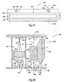
- Figure 2 illustrates a cross-sectional view of how the transparent material 32 may be secured to the scanner casing 20.
- figure 2 shows how the casing 20 can be manufactured to provide a scan window 22A, 22B that includes a ledge for supporting the transparent material 32 with an adhesive 36.
- the transparent material 32 is positioned a depth "d", between 0.02 - 0.05 mm, away from an outer surface 38 of the casing 20 to create a recessed border defined by square comer regions 40.
- the recessed border is not deep enough to prevent a staple or a hard particle contained on an object from scratching the transparent material while the object is being scanned.
- the square corner regions 40 collect dust and other contaminants in areas that are hard to clean. Consequently, the scratches and collected contaminants further increase optical losses in the operational scanner. In turn, such optical losses may force the user to have the manufacturer replace the transparent material, which is not only time consuming, but costly.
- the square comer regions 40 may cause the comers of the object being scanned to become jammed along the recessed borders of the scan window during the scanning process.
- the present invention seeks to provide improved optical scanning.
- an optical scanner as specified in claim 1.
- an optical scanner having a casing.
- the casing includes a scan window, a substrate attached with the casing and being laterally spaced from the scan window, and an optics module coupled between the scan window and the substrate to form a recess within the casing.
- a method of manufacturing a recessed scan window for use in an optical scanning apparatus having a casing includes: forming a contact window within a scan surface of the apparatus casing; securing a substrate within the apparatus casing; coupling a first end of an illumination device to the substrate and a second end adjacent to a first portion of the contact window; and coupling a first end of a photosensor component to the substrate and a second end adjacent to a second portion of the contact window, wherein the second end of the illumination device and the photosensor component forms the recessed scan window.
- the described embodiment seeks to provide an efficient, effective and reliable means for a photoelectric imaging system to obtain machine-readable data, which represents an image on an object, e.g. a page of printed text. More specifically, it provides an optics module for a portable scanner having an illumination and photosensor component coupled between a substrate and a scan window.
- the illumination component creates a beam of light that can pass through the scan window and reflect off a portion of an object (“scan line") being positioned under the scan window.
- the reflected beam of light passes back through the scan window before being received by the photosensor component and evaluated/manipulated by complimentary imaging electronics and software.
- optical loss in the embodiments described are significantly less than the optical loss in conventional optic modules because their optics module allows for the beam of light to pass and reflect through the scan window without having to pass through a transparent material. This is possible because the structure uses the components of the optics module to define a recess within the scan window that can prevent the electronic components of the portable scanner from operational contaminants or scratching. By eliminating the use of the transparent material, the optics module is less expensive to manufacture and dimensionally smaller in size. The structure for the optics module can be similarly used for a navigational assembly of the optics module.
- figure 3 illustrates an embodiment of a portable scanner 110.
- the hand-held scanner 110 may be used to scan an image 118 of object 114, such as a piece of paper having a surface 116 with written text thereon.
- the image 118 is scanned by moving the scanner 110 over the document surface 116 in a scan direction generally indicated by arrow 120.
- the hand-held scanner 110 may include an elongated housing or casing 122 for containing the various internal components and systems required for the operation of the scanner, as will be described in greater detail below.
- the front side 123 of casing 122 may include a display 128, such as a liquid crystal display ("LCD”), for displaying data and/or function options of the scanner.
- the front side 123 may provide a plurality of function buttons 130, scrolling buttons 132, an enter button 134, a scan button 135 and an on/off switch 136.
- the buttons 130 may be used to control the various functions of the hand scanner 110 including: to initiate and terminate scanning of the image 118, to transfer a scanned image to a computer being coupled by a data cable, to zoom in or out of the displayed image, and to delete a scanned image from memory.
- the interior 146 of casing 122 is adapted to receive the optics module 150, the LCD 128, a power source 156, and an image processing system ("IPS") 158.
- the optics module 150 includes a scanning assembly 159 and an area 170 for containing a navigational assembly 174, if desired (see figures 6B or 7B).
- the optics module does not require a navigational assembly to operate, nor does the navigational assembly take-up as much room in the casing 122 as the scanning assembly 159.
- the scanning assembly 159 illuminates a scanning region or scan line 152 with an array of light emitting diodes ("LEDs") 160 and a light guide 162.
- the scanning region 152 is within a scan window 164 of scanning surface 138.
- the light used to illuminate the scan region 152 is reflected off of the document surface 116 and received by a lens 166.
- the lens 166 carries the reflected light to photosensor 168.
- the IPS 158 (a block diagram of which is illustrated in figure 8) receives data signals from the photosensor device 168 and processes the data signals as necessary to produce digital image data that the user can view on the display 128.
- the IPS 158 may also control the other functions and operations of the scanner 110, as described above.
- the above components are coupled to one another in a conventional manner.
- the casing 122 of scanner 110 may be manufactured by a conventional method, such as injection molding and include other components and/or systems that may be necessary or desirable for the hand scanner apparatus 110 to operate.
- the scanning surface 138 and optics module 150 are shown.
- the scanning surface 138 provides a scan window 164 for the scanning assembly 159 and a navigational window 176 for the navigational assembly 174.
- the scan window 164 provides a recess 165 being defined by the scanning window 164, the light guide 162, the lens 166 and the reflective material 178 on either side of the light guide and lens.
- the navigational window 176 provides a recess 177 being defined by navigational window 176, the light source 182, the lens 184 and the reflective material 178 on either side of the light source and lens.
- the navigational assembly 174 is laterally separated from the scanning assembly 159 by the reflective material 178 being coupled between the casing 122 and substrate 196.
- the illumination source 160 produces a ray of light that follows a light path 1.
- the light path 1 internally reflects from the sides of the solid light pipe and follows reflected light paths 1' out of the solid light pipe and optics module 150 to a scan region 152 under the lens 166.
- Image light 1' being reflected from the object 114, travels along a light path r where it is focused by the lens 166, such as a "SELFOC" lens, before reaching the photosensor 168.
- the optical detector 168 produces electrical signals representative of the image light for the IPS 158 (see figure 4) to process and manipulate for display or downloading.
- each light source 182 such as an LED, creates a beam of light (“'Nl") that is reflected off of the document surface 116 in a direction parallel with the length ("Nl") of scan window 164.
- the navigational sensor 186 receives the reflected light ("Nr") through the navigational lens 184.
- the navigational sensor 186 uses the reflected light ("Nr") to provide position information, which is paired with the swaths of image data provided by the optical detector 168.
- a stitching algorithm can then use the position information to create a complete image of the object 114 from the scanned image swaths.
- the optics module 300 rotates the navigational window 176 and recess 170 of figures 5A and 5B by 90 degrees. This rotation allows the lens 166 of the scanning assembly 159 to receive the light beam of the navigational light source 182 after being reflected off of the document surface 116 being scanned.
- the known properties of a "SELFOC" lens are used to separate and guide the reflected light beams of the scanning assembly and navigational assembly to their respective photosensors 168 and 186.
- the same components and structure is used for the scanning assembly as described above, however the navigational lens 184 is eliminated for the navigational assembly and the navigational scan path is rotated 90 degrees.
- the illumination sources 160 and 182 produce a ray of light that follows a light path 1 and Nl, respectively.
- light produced by illumination source 160 is captured by light guide 162.
- the captured light internally reflects from the sides of the light guide to follow light paths 1 and 1' out of the solid light pipe, through the scan window 364 and onto a scan region 352 under the lens 166.
- the light from the navigational light source follows the light path Nl through the scan window 364 and onto a scan region 352 under the lens 166. Consequently, light from each illumination source 160 and 182 follows a light path r and Nr, respectively, through the lens 166 to the optical detectors 168 and 186.
- the known properties of the lens 166 allows for each source of light entering into the lens at a different angle to be captured by their respective photosensor 168 and 186 upon their exit from the lens.
- the optical detectors 168 and 186 transfer the reflected light to the IPS 158 so that electrical signals can be produced to represent the image light.
- the above embodiment allows for further cost and space reductions over the first embodiment by eliminating the need for a navigational lens 184 and window 176 (see figures 5A and 5B). Consequently, less space is needed on the substrate 196, less reflective material 178 will be used, and the weight and power consumption of the scanner will be reduced.
- the reflective material used in the above embodiment is conventional, such as a black plastic, and couples to the distal end of the scanning and navigational assembly components by a conventional method to seal each recess from contaminants reaching any other surface of the components contained by the casing 122.
- the reflective material provides a smooth radii surface structure within each recess to avoid the accumulation of dust or other contaminants from gathering at the inner corners 190, to provide easy cleaning, and to prevent the edge of a document surface 116 (see figure 4) from catching on the outer corners 192 while being scanned (see figure 4 and SB).
- the reflective or containing material 178 could be removed so that only the lens 166 and light guide would define the recess of the scan window.
- the width ("W") of the scan windows 164 and 364 is approximately 1-4 mm for the length ("L") of the scanning region 152. This distance is wide enough to permit a scan line of data to be obtained, but sufficiently narrow to prevent the document from bowing up into the recess portion 165.
- the depth "D" of the recessed portions 165 and 365 is between about 1.5 and 5 mm. This depth should eliminate the chance of a staple or a particle on the document surface 116 from scratching any component of the scanning assembly.
- the width and length of the navigational windows 176 in figures 5A and 5B is much smaller than the width and length of the scanning windows 164 and 364. This is primarily due to the fact that the navigational windows 176 are laterally spaced from each other along the length "L" of the scanning window 164. In turn, the navigational window 176 only has to accommodate a light beam "Nl" from a single LED 182 that reflects off of the object 114 in the direction of the length "L” before being received by a navigational lens that feeds the reflected light "Nr" to the navigational photosensor 186.
- the depth of the navigational window 176 i.e., the distance from the scanning surface 138 to the surface of the lens 184 closest to the scanning surface 138) maybe between about 3 to 5 mm.
- the image detectors or photosensors 168 and 186 and the illumination sources 160 and 182 mount to a single substrate 196, such as a printed circuit board ("pcb").
- the printed circuit board 196 is preferably mounted to the casing 122, which provides a compact structure for the optics module 150.
- the pcb 196 may also include a plurality of conductors, such as printed circuit paths (not shown), to electrically connect the various LEDs 160 to a suitable connector node or pad (not shown) on pcb 196.
- the connector node or pad (not shown) in turn may be connected to a suitable LED driver circuit, such as a pulse width modulation circuit, by any of a wide variety of electrical conductors, such as flexible insulated wire, etc.
- pcb 196 may include a pair of spot-light LEDs 182 for the navigational assembly 177.
- the illuminaton source 160 may include an array of light emitting diodes ("LEDs") arranged along an elongate surface of the pcb 196.
- the lens 166 for the scanning assembly is preferably a "SELFOC" lens, manufactured by NSG ("Nippon Sheet Glass”).
- the lens 184 for the navigational assembly of the embodiment of figures 5A and 5B is preferably a conventional bi-convex single element imaging lens made by plastic injection molding from materials such as acrylic polycarbonate. Each lens directs and focuses reflected light from the object 114 onto the optical detector 168.
- the photo sensor 168 is a conventional CMOS linear array.
- the light guide 162 positioned under the illumination source 160, is mounted to the lens 164 and the casing 122.
- the light guide 162 comprises a solid light pipe.
- the solid light pipe may be made from any substantially transparent material having an index of refraction greater than that of air. As a result of the index of refraction, light rays may pass into and out of the solid light pipe only when the rays are at near normal angles with respect to the sides of the light pipe. Any light rays striking the sides of the solid light pipe with angles of incidence greater than the critical angle of incidence for the light pipe material will be internally reflected.
- the top of the solid light pipe is perpendicular to the preferred direction of illumination of the scan region, such as along the illustrated reflected light path. Stray light baffles or reflectors may be placed alongside the illumination source to direct the light rays into the solid light pipe. In addition, the top of the solid light pipe may be slightly textured if desired to diffuse the light from the illumination source 160 as it enters the light pipe. For further details about light guides that may be used see, for example, U.S. Pat. Appl. Ser. No. 09/477,205 of David Bohn for "Contact Image Sensor With Light Guide," which is hereby incorporated by reference for all that it discloses.
- the image processing system 158 may comprise a microprocessor assembly 400 conventionally coupled to a memory system 402 for collecting and processing the image data provided by the scanning and navigational photosensors 168 and 186.
- the various function buttons 130, scrolling buttons 132, enter button 134, scan button 135, and on/off switch 136 are also connected to the microprocessor 400 having a power supply 156, such as two 'AA' or 'AAA' batteries or power cord.
- the various buttons interact with a software program executed by the microprocessor 400 to control the various functions and operations of the scanner 110.
- the display system 128 is also connected to the microprocessor 400 and may be used to show the user data relating to the scanning operation.
- the photosensors 168 and 186 are also connected to the microprocessor 400 having an input/output (I/O) port 406 to allow data to be exchanged with external devices, such as a computer (not shown).
- I/O port 406 may comprise a standard serial or USB port or may comprise an infrared port.
- the optics module for a scanning apparatus can produce a quality digital image of a scanned object.
- the IPS will activate the scanning processes as described above. If the length ("L") of the scanning window 164 is not as wide as the object 114 to be scanned, the optics module 150 is swept over the object 114 in a curvilinear or meandering fashion during a scanning operation. This sweeping action produces connected image strips or swaths which must then be stitched together by a stitching algorithm to produce a complete image of the object 114.
- the optics module of the above embodiments may be used in any imaging device such as a scanner or fax machine to capture the image of an object.
- the structure eliminates the need for a transparent material to be positioned between the document surface and the components of the optics module. Consequently, the user will not experience optical losses due to particles or staples on the document surface that typically scratch a transparent material used to seal the casing and protect the components of the optics module.
- the combination of the depth, narrow width and smooth radii at the corners of the recessed scan window permits the scan surface to flatten the document without the document bowing into the recessed window and helps to prevent dust particles from accumulating in the recessed scan window. If contaminants do collect, the user can easily clean the recessed scan window.
- the LEDs typically radiate light over a very wide range of directions, most of which are not aimed at the scan line.
- the light guide redirects this light toward the scan line.
- the light guide reduces stray light inside the optics module and provides improved depth of illumination of the scan region on the object.
- the optics module having the light guide directs the light from the illumination source onto the scan region so that even if the optics module is tilted or moved slightly away from the object, the image does not darken as rapidly. Since the light is more focused and directed toward the scan region, the flux per unit angle is greater and the intensity does not drop off as quickly with an increase in distance from the illumination source.
- the light guide also reduces the non-uniformed spot-light effect which increases with distance as a conventional optics module is moved away from the object.
- the optics module can be more compact and less expensive than previous optics modules. Without a light guide, the illumination source is typically mounted on a separate circuit board that is positioned close to the scan region at an angle. In addition, a transparent material is positioned within the scan window of the casing to protect the closely positioned illumination source.
- the light guide removes the need for an additional circuit board, with its attendant wires, electrical interconnect and mounting hardware, and the need for the transparent material that can be easily scratched and collect contaminants.
- the optics module with a light guide and without a transparent material is thus simpler to assemble, costs less, and is less prone to failure.
- the optics module with a light guide allows a smaller and lighter scanner, fax machine, or other imaging device.
Landscapes
- Engineering & Computer Science (AREA)
- Multimedia (AREA)
- Signal Processing (AREA)
- Facsimile Scanning Arrangements (AREA)
- Image Input (AREA)
- Facsimile Heads (AREA)
Applications Claiming Priority (2)
| Application Number | Priority Date | Filing Date | Title |
|---|---|---|---|
| US541171 | 2000-04-03 | ||
| US09/541,171 US6426498B1 (en) | 2000-04-03 | 2000-04-03 | Optics module for optical scanning device |
Publications (2)
| Publication Number | Publication Date |
|---|---|
| EP1143697A2 true EP1143697A2 (fr) | 2001-10-10 |
| EP1143697A3 EP1143697A3 (fr) | 2002-06-19 |
Family
ID=24158467
Family Applications (1)
| Application Number | Title | Priority Date | Filing Date |
|---|---|---|---|
| EP01302083A Withdrawn EP1143697A3 (fr) | 2000-04-03 | 2001-03-07 | Dispositif de balayage optique |
Country Status (3)
| Country | Link |
|---|---|
| US (1) | US6426498B1 (fr) |
| EP (1) | EP1143697A3 (fr) |
| JP (1) | JP2002010038A (fr) |
Cited By (1)
| Publication number | Priority date | Publication date | Assignee | Title |
|---|---|---|---|---|
| EP3043545A1 (fr) * | 2015-01-06 | 2016-07-13 | Foxlink Image Technology Co., Ltd. | Scanner de poche |
Families Citing this family (6)
| Publication number | Priority date | Publication date | Assignee | Title |
|---|---|---|---|---|
| US7333083B1 (en) * | 2001-05-10 | 2008-02-19 | Logitech Europe S.A. | Optical based performance improvement for an optical illumination configuration |
| US7012234B2 (en) * | 2002-12-13 | 2006-03-14 | Hewlett-Packard Development Company, L.P. | Apparatus and method for capturing oversize images for imaging devices |
| US20040227059A1 (en) * | 2003-05-14 | 2004-11-18 | Spears Kurt E. | Compact integrated optical imaging assembly |
| US7208719B2 (en) * | 2003-05-14 | 2007-04-24 | Hewlett-Packard Development Company, L.P. | Compact integrated optical imaging assembly |
| US7346206B2 (en) * | 2003-06-20 | 2008-03-18 | Hewlett-Packard Development Company, L.P. | Optical object detector |
| US20080266894A1 (en) * | 2007-04-24 | 2008-10-30 | Hosein Ali Razavi | Imaging device illumination system |
Family Cites Families (11)
| Publication number | Priority date | Publication date | Assignee | Title |
|---|---|---|---|---|
| US5272518A (en) * | 1990-12-17 | 1993-12-21 | Hewlett-Packard Company | Colorimeter and calibration system |
| US5306908A (en) | 1993-03-15 | 1994-04-26 | Hewlett-Packard Company | Manually operated hand-held optical scanner with tactile speed control assembly |
| US5381020A (en) | 1993-03-31 | 1995-01-10 | Hewlett-Packard Company | Hand-held optical scanner with onboard battery recharging assembly |
| US5412205A (en) * | 1993-11-18 | 1995-05-02 | Logitech, Inc. | Scanner with a wing-shaped fluorescent tube housing and dual-faceted scan window |
| FR2714751B1 (fr) * | 1994-01-04 | 1996-03-29 | Int Jeux | Dispositif anti-encrassement pour écran de transmission de lumière entre un support d'informations éclairé par une source lumineuse et des éléments de lecture. |
| US5578813A (en) | 1995-03-02 | 1996-11-26 | Allen; Ross R. | Freehand image scanning device which compensates for non-linear movement |
| US5936238A (en) | 1997-10-29 | 1999-08-10 | Hewlett-Packard Company | Portable optical scanning device with a recessed optical window |
| US6002124A (en) | 1998-03-20 | 1999-12-14 | Hewlett-Packard Company | Portable image scanner with optical position sensors |
| US6154294A (en) * | 1998-07-16 | 2000-11-28 | Silitek Corporation | Apparatus for scanning documents such as photographs using a contact image sensor |
| WO2000014949A1 (fr) * | 1998-09-09 | 2000-03-16 | Rohm Co., Ltd. | Lecteur d'image |
| US6229137B1 (en) * | 1998-09-14 | 2001-05-08 | Hewlett-Packard Company | Scan line illumination system utilizing hollow reflector |
-
2000
- 2000-04-03 US US09/541,171 patent/US6426498B1/en not_active Expired - Fee Related
-
2001
- 2001-03-07 EP EP01302083A patent/EP1143697A3/fr not_active Withdrawn
- 2001-04-03 JP JP2001105157A patent/JP2002010038A/ja active Pending
Cited By (1)
| Publication number | Priority date | Publication date | Assignee | Title |
|---|---|---|---|---|
| EP3043545A1 (fr) * | 2015-01-06 | 2016-07-13 | Foxlink Image Technology Co., Ltd. | Scanner de poche |
Also Published As
| Publication number | Publication date |
|---|---|
| JP2002010038A (ja) | 2002-01-11 |
| US6426498B1 (en) | 2002-07-30 |
| EP1143697A3 (fr) | 2002-06-19 |
Similar Documents
| Publication | Publication Date | Title |
|---|---|---|
| US5586212A (en) | Optical wave guide for hand-held scanner | |
| KR100668361B1 (ko) | 지문 이미지 광 입력장치 | |
| US6628335B1 (en) | Image capture module and image capture apparatus for inputting shape of object on three dimensional space | |
| US5552597A (en) | Hand-held scanner having adjustable light path | |
| US6724503B1 (en) | Image sensor substrate and image sensor employing it | |
| JP3272600B2 (ja) | データシンボル読み取り装置 | |
| US6064062A (en) | Optical stray light baffle for image scanner | |
| EP1193641B1 (fr) | Structure de fabrication bon marché et compacte pour un lecteur de codes à barres | |
| US5121226A (en) | Portable image scanner | |
| US6426498B1 (en) | Optics module for optical scanning device | |
| US5019918A (en) | Portable image scanner | |
| US5763866A (en) | Optical reader for information pattern representing coded data | |
| US5936238A (en) | Portable optical scanning device with a recessed optical window | |
| EP0785664A2 (fr) | Dispositif de balayage avec composants optiques sans contact | |
| US20030063333A1 (en) | Flatbed scanner with apparatus for scanning light transmissive objects | |
| EP0886161A2 (fr) | Dispositif de balayage avec fenêtre flottante | |
| JPH08119493A (ja) | 原稿端検知装置 | |
| TWI495324B (zh) | 光學系統及應用該光學系統的掃描器 | |
| JP2002109464A (ja) | 情報コード読取装置 | |
| JPS62296652A (ja) | 画像読取装置 | |
| JPH05308474A (ja) | 画像読取り装置 | |
| WO2004021278A1 (fr) | Element optique et dispositif de lecture | |
| JPH07131608A (ja) | イメージセンサ | |
| JPH07307833A (ja) | イメージセンサー及びそれを用いた情報処理装置 | |
| JPH03267860A (ja) | 光学式画像読取装置 |
Legal Events
| Date | Code | Title | Description |
|---|---|---|---|
| PUAI | Public reference made under article 153(3) epc to a published international application that has entered the european phase |
Free format text: ORIGINAL CODE: 0009012 |
|
| AK | Designated contracting states |
Kind code of ref document: A2 Designated state(s): AT BE CH CY DE DK ES FI FR GB GR IE IT LI LU MC NL PT SE TR |
|
| AX | Request for extension of the european patent |
Free format text: AL;LT;LV;MK;RO;SI |
|
| PUAL | Search report despatched |
Free format text: ORIGINAL CODE: 0009013 |
|
| AK | Designated contracting states |
Kind code of ref document: A3 Designated state(s): AT BE CH CY DE DK ES FI FR GB GR IE IT LI LU MC NL PT SE TR |
|
| AX | Request for extension of the european patent |
Free format text: AL;LT;LV;MK;RO;SI |
|
| RIC1 | Information provided on ipc code assigned before grant |
Free format text: 7H 04N 1/107 A, 7H 04N 1/031 B |
|
| 17P | Request for examination filed |
Effective date: 20020902 |
|
| AKX | Designation fees paid |
Designated state(s): DE FR GB |
|
| 17Q | First examination report despatched |
Effective date: 20060719 |
|
| STAA | Information on the status of an ep patent application or granted ep patent |
Free format text: STATUS: THE APPLICATION IS DEEMED TO BE WITHDRAWN |
|
| 18D | Application deemed to be withdrawn |
Effective date: 20070130 |