EP1143776B1 - Carte a circuit imprime et procede de fabrication correspondant - Google Patents
Carte a circuit imprime et procede de fabrication correspondant Download PDFInfo
- Publication number
- EP1143776B1 EP1143776B1 EP99931459A EP99931459A EP1143776B1 EP 1143776 B1 EP1143776 B1 EP 1143776B1 EP 99931459 A EP99931459 A EP 99931459A EP 99931459 A EP99931459 A EP 99931459A EP 1143776 B1 EP1143776 B1 EP 1143776B1
- Authority
- EP
- European Patent Office
- Prior art keywords
- conductor pattern
- substrate
- circuit board
- width
- printed circuit
- Prior art date
- Legal status (The legal status is an assumption and is not a legal conclusion. Google has not performed a legal analysis and makes no representation as to the accuracy of the status listed.)
- Expired - Lifetime
Links
Images


Classifications
-
- H—ELECTRICITY
- H05—ELECTRIC TECHNIQUES NOT OTHERWISE PROVIDED FOR
- H05K—PRINTED CIRCUITS; CASINGS OR CONSTRUCTIONAL DETAILS OF ELECTRIC APPARATUS; MANUFACTURE OF ASSEMBLAGES OF ELECTRICAL COMPONENTS
- H05K3/00—Apparatus or processes for manufacturing printed circuits
- H05K3/22—Secondary treatment of printed circuits
- H05K3/28—Applying non-metallic protective coatings
-
- H—ELECTRICITY
- H05—ELECTRIC TECHNIQUES NOT OTHERWISE PROVIDED FOR
- H05K—PRINTED CIRCUITS; CASINGS OR CONSTRUCTIONAL DETAILS OF ELECTRIC APPARATUS; MANUFACTURE OF ASSEMBLAGES OF ELECTRICAL COMPONENTS
- H05K3/00—Apparatus or processes for manufacturing printed circuits
- H05K3/30—Assembling printed circuits with electric components, e.g. with resistors
- H05K3/32—Assembling printed circuits with electric components, e.g. with resistors electrically connecting electric components or wires to printed circuits
- H05K3/34—Assembling printed circuits with electric components, e.g. with resistors electrically connecting electric components or wires to printed circuits by soldering
- H05K3/3452—Solder masks
-
- H—ELECTRICITY
- H05—ELECTRIC TECHNIQUES NOT OTHERWISE PROVIDED FOR
- H05K—PRINTED CIRCUITS; CASINGS OR CONSTRUCTIONAL DETAILS OF ELECTRIC APPARATUS; MANUFACTURE OF ASSEMBLAGES OF ELECTRICAL COMPONENTS
- H05K2201/00—Indexing scheme relating to printed circuits covered by H05K1/00
- H05K2201/09—Shape and layout
- H05K2201/09209—Shape and layout details of conductors
- H05K2201/09654—Shape and layout details of conductors covering at least two types of conductors provided for in H05K2201/09218 - H05K2201/095
- H05K2201/098—Special shape of the cross-section of conductors, e.g. very thick plated conductors
-
- H—ELECTRICITY
- H05—ELECTRIC TECHNIQUES NOT OTHERWISE PROVIDED FOR
- H05K—PRINTED CIRCUITS; CASINGS OR CONSTRUCTIONAL DETAILS OF ELECTRIC APPARATUS; MANUFACTURE OF ASSEMBLAGES OF ELECTRICAL COMPONENTS
- H05K2203/00—Indexing scheme relating to apparatus or processes for manufacturing printed circuits covered by H05K3/00
- H05K2203/05—Patterning and lithography; Masks; Details of resist
- H05K2203/0562—Details of resist
- H05K2203/0594—Insulating resist or coating with special shaped edges
-
- H—ELECTRICITY
- H05—ELECTRIC TECHNIQUES NOT OTHERWISE PROVIDED FOR
- H05K—PRINTED CIRCUITS; CASINGS OR CONSTRUCTIONAL DETAILS OF ELECTRIC APPARATUS; MANUFACTURE OF ASSEMBLAGES OF ELECTRICAL COMPONENTS
- H05K2203/00—Indexing scheme relating to apparatus or processes for manufacturing printed circuits covered by H05K3/00
- H05K2203/05—Patterning and lithography; Masks; Details of resist
- H05K2203/0562—Details of resist
- H05K2203/0597—Resist applied over the edges or sides of conductors, e.g. for protection during etching or plating
-
- H—ELECTRICITY
- H05—ELECTRIC TECHNIQUES NOT OTHERWISE PROVIDED FOR
- H05K—PRINTED CIRCUITS; CASINGS OR CONSTRUCTIONAL DETAILS OF ELECTRIC APPARATUS; MANUFACTURE OF ASSEMBLAGES OF ELECTRICAL COMPONENTS
- H05K3/00—Apparatus or processes for manufacturing printed circuits
- H05K3/30—Assembling printed circuits with electric components, e.g. with resistors
- H05K3/32—Assembling printed circuits with electric components, e.g. with resistors electrically connecting electric components or wires to printed circuits
- H05K3/34—Assembling printed circuits with electric components, e.g. with resistors electrically connecting electric components or wires to printed circuits by soldering
- H05K3/3465—Application of solder
-
- H—ELECTRICITY
- H10—SEMICONDUCTOR DEVICES; ELECTRIC SOLID-STATE DEVICES NOT OTHERWISE PROVIDED FOR
- H10W—GENERIC PACKAGES, INTERCONNECTIONS, CONNECTORS OR OTHER CONSTRUCTIONAL DETAILS OF DEVICES COVERED BY CLASS H10
- H10W72/00—Interconnections or connectors in packages
- H10W72/01—Manufacture or treatment
- H10W72/012—Manufacture or treatment of bump connectors, dummy bumps or thermal bumps
- H10W72/01251—Changing the shapes of bumps
- H10W72/01255—Changing the shapes of bumps by using masks
-
- H—ELECTRICITY
- H10—SEMICONDUCTOR DEVICES; ELECTRIC SOLID-STATE DEVICES NOT OTHERWISE PROVIDED FOR
- H10W—GENERIC PACKAGES, INTERCONNECTIONS, CONNECTORS OR OTHER CONSTRUCTIONAL DETAILS OF DEVICES COVERED BY CLASS H10
- H10W72/00—Interconnections or connectors in packages
- H10W72/20—Bump connectors, e.g. solder bumps or copper pillars; Dummy bumps; Thermal bumps
- H10W72/241—Dispositions, e.g. layouts
- H10W72/242—Dispositions, e.g. layouts relative to the surface, e.g. recessed, protruding
-
- H—ELECTRICITY
- H10—SEMICONDUCTOR DEVICES; ELECTRIC SOLID-STATE DEVICES NOT OTHERWISE PROVIDED FOR
- H10W—GENERIC PACKAGES, INTERCONNECTIONS, CONNECTORS OR OTHER CONSTRUCTIONAL DETAILS OF DEVICES COVERED BY CLASS H10
- H10W72/00—Interconnections or connectors in packages
- H10W72/20—Bump connectors, e.g. solder bumps or copper pillars; Dummy bumps; Thermal bumps
- H10W72/29—Bond pads specially adapted therefor
-
- H—ELECTRICITY
- H10—SEMICONDUCTOR DEVICES; ELECTRIC SOLID-STATE DEVICES NOT OTHERWISE PROVIDED FOR
- H10W—GENERIC PACKAGES, INTERCONNECTIONS, CONNECTORS OR OTHER CONSTRUCTIONAL DETAILS OF DEVICES COVERED BY CLASS H10
- H10W72/00—Interconnections or connectors in packages
- H10W72/90—Bond pads, in general
- H10W72/941—Dispositions of bond pads
- H10W72/9415—Dispositions of bond pads relative to the surface, e.g. recessed, protruding
-
- H—ELECTRICITY
- H10—SEMICONDUCTOR DEVICES; ELECTRIC SOLID-STATE DEVICES NOT OTHERWISE PROVIDED FOR
- H10W—GENERIC PACKAGES, INTERCONNECTIONS, CONNECTORS OR OTHER CONSTRUCTIONAL DETAILS OF DEVICES COVERED BY CLASS H10
- H10W74/00—Encapsulations, e.g. protective coatings
- H10W74/10—Encapsulations, e.g. protective coatings characterised by their shape or disposition
- H10W74/131—Encapsulations, e.g. protective coatings characterised by their shape or disposition the semiconductor body being only partially enclosed
- H10W74/137—Encapsulations, e.g. protective coatings characterised by their shape or disposition the semiconductor body being only partially enclosed the encapsulations being directly on the semiconductor body
Definitions
- the present invention relates to a printed circuit board and a method of manufacturing same, and more particularly, to a printed circuit board provided with a conductor pattern having superior adhesion and a method of manufacturing same.
- a prior art printed circuit board 9 is shown in Fig. 5(A).
- the printed circuit board 9 includes an insulative substrate 2, a plurality of conductor patterns 93, and an insulative protection film 94 coating the substrate 2 and the patterns 93.
- the conductor patterns 93 function as wiring and external terminals.
- the bottom surfaces 931 of the conductor patterns 93 are adhered to the upper surface of the substrate 2.
- the width a of the bottom surface 931 is equal to the width b of the top surface 932 of the conductor pattern 93.
- the conductor patterns 93 have rectangular cross-sections.
- the side surfaces 935 of the conductor patterns 93 are completely coated by the protection film 94.
- the conductor patterns 93 are formed after forming the protection film 94 on the substrate 2.
- the conventional conductor patterns 93 have a rectangular cross-section in which the width a of the bottom surface 931 is equal to the width b of the top surface 932, the area of contact between the conductor patterns 93 and the substrate 2 is relatively small. Hence, the adhesion between the substrate 2 and the conductor patterns 93 is relatively weak. Accordingly, as shown in Fig. 5(B), when an external force, such as thermal stress, is applied to the printed circuit board 9, the conductor patterns 93 may be separated from the upper surface of the substrate 2.
- the conductor patterns 93 may have a trapezoid cross-section in which the width a of the bottom surface 931 is greater then the width b of the top surface 932 (see documents US-A-5 766 674 and JP-A-5 206 209).
- the material forming the conductor patterns 93 forces the protection film 4, which is shaped in correspondence with the conductor patterns 93, upward.
- the protection film 94 may be separated from the upper surface of the substrate 2. Further, as shown in Fig.
- a portion 939 of the conductor patterns 93 may enter the space between the bottom surface of the protection film 94 and the upper surface of the substrate 2 causing a short-circuit with the adjacent conductor pattern 93.
- the side surfaces 935 of the conductor pattern 93 are completely coated by the protection film 94.
- the solder ball 96 is not hooked to the side surfaces 935 of the conductor pattern 93. Accordingly, if a lateral force, such as that indicated by an arrow, is applied to the solder ball 96, the solder ball 96 may be separated from the conductor pattern 93.
- the side surfaces 935 of the conductor pattern 93 may be completely exposed to allow the solder ball 96 to enter the space between the side surfaces 935 of the conductor pattern 93 and the protection film 94.
- the solder ball 96 contacts the substrate 2, which mechanical strength is relatively weak. Due to the surface tension of the solder ball, the area of the contact portion between the solder ball 96 and the substrate 2 is relatively small. Therefore, when a lateral force, such as that indicated by the arrow, is applied to the solder ball 96, the force is locally applied to the contact portion of the substrate 2. As a result, a crack 99 may be produced in the substrate 2, and the substrate 2 may be damaged.
- a first aspect of the present invention provides a printed circuit board including a substrate, a conductor pattern formed on the substrate, and a protection film coating the substrate and the conductor pattern.
- the conductor pattern includes a bottom surface contacting the substrate, a top surface opposite to the bottom surface, and a pair of side surfaces. Each of the side surfaces have a lower side surface covered by the protection film and an upper side surface exposed from the protection film. The width of the bottom surface is greater than the width of the top surface.
- the width of the bottom surface of the conductor pattern be greater than the width of the top surface, the lower side surface be coated by the protection film, and the upper side surface be exposed from the protection film.
- the width of the bottom surface of the conductor pattern is greater than the width of the top surface, and the area of the portion adhered to the substrate is relatively large. Accordingly, in comparison with a conductor pattern having a rectangular cross-section, the adhesion between the substrate and the conductor pattern is stronger. Thus, separation of the conductor pattern from the upper surface of the substrate is prevented.
- the upper side surfaces of the conductor pattern are exposed from the protection film.
- the solder ball enters the upper side surfaces of the conductor pattern.
- the solder ball has a portion hooked to the side surfaces thereby preventing the solder ball from being separated from the conductor pattern.
- the lower side surface of the conductor pattern is coated by the protection film. Accordingly, for example, the solder ball contacts the conductor pattern, which mechanical strength is greater than that of the substrate, without contacting the substrate. Thus, even if a lateral force is applied to the solder ball subsequent to the joining, the force acts on the conductor pattern and not on the substrate thereby preventing damages, such as cracking, of the substrate.
- the top surface of the conductor pattern be coated by a plating. In this case, the solder ball is easily joined to the conductor pattern.
- solder ball contact the conductor pattern at the upper side surfaces of the conductor pattern. In this case, even if a lateral force is applied to the joined solder ball, the solder ball is in contact with the side surfaces of the conductor pattern and thus separation of the solder ball from the conductor pattern is prevented.
- a second aspect of the present invention provides a method for fabricating a printed circuit board.
- the method includes the steps of etching a substrate including a conductor to form a conductor pattern, applying an insulative protection film to the conductor pattern and the substrate, and removing part of the protection film.
- the conductor pattern is formed so that a width of a bottom surface contacting the substrate is greater than a width of a top surface, which is opposite the bottom surface.
- an upper portion of the conductor pattern is exposed.
- the conductor pattern is formed before the protection film. Accordingly, the protection film does not exist when the conductor pattern is formed. Thus, the conductor pattern does not force the protection film upward. Further, part of the conductor pattern does not enter the space between the bottom surface of the protection film and the top surface of the substrate. As a result, short-circuiting between adjacent conductor patterns is prevented.
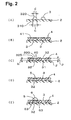
- a printed circuit board according to a first embodiment of the present invention will now be described with reference to Figs. 1 and 2.
- the printed circuit board 1 includes a insulative substrate 2, a conductor pattern 3 formed on the substrate 2, and an insulative protection film, or solder resist 4, for coating the substrate 2 and the conductor pattern 3.
- the conductor pattern 3 extends perpendicular to the plane of the drawing. As shown in Fig. 1, the conductor pattern 3 includes an upper portion 32 and a lower portion 31. The bottom surface 310 of the conductor pattern 3 is adhered to the upper surface of the substrate 2. The width c of the bottom surface 310 is greater than the width d of the top surface 320. Accordingly, the conductor pattern 3 has a trapezoidal cross-section, which is perpendicular to the longitudinal direction. The side surfaces 315 of the lower portion 31 are coated by the solder resist 4.
- the side surfaces 325 of the upper portion 32 are not coated by the solder resist 4.
- the height h of the lower portion 31 is 95% of the conductor pattern height p.
- the remaining 5% of the conductor pattern height p is the height of the upper portion 32.
- the top surface 320 of the upper portion 32 and the side surfaces 325 are coated by a connection terminal plating 5.
- a solder ball 6 is connected to the conductor pattern 3 by the plating 5. The solder ball 6 engages the side surfaces 325 of the upper portion 32.
- the printed circuit board 1 is fabricated from a copperclad laminate, which is produced by cladding a copper foil on the substrate 2.
- the copperclad laminate undergoes etching to form a plurality of conductor patterns 3 on the substrate 2.
- the conductor pattern 3 is formed so that its cross-section is a trapezoid, which width c of the bottom surface 310 is greater than the width d of the top surface 320. It is preferred that the width c of the bottom surface 310 be 30 to 200pm and the width d of the top surface 320 be 10 to 180 ⁇ m. In the first embodiment, the width c of the bottom surface 310 is 80 ⁇ m, the width d of the top surface 320 is 70 ⁇ m, and the height p of the conductor pattern 3 is 35 ⁇ m.
- the solder resist 4 is applied so as to entirely cover the conductor patterns 3 and the substrate 2.
- the solder resist 4 is applied so that the height of the solder resist 4 is generally constant, or such that its surface 41 is flat.
- a laser is irradiated against the upper surface 41 of the solder resist 4 to remove the solder resist 4 along the conductor pattern 3, as shown in Fig. 2(C).
- the laser irradiation is stopped when 5% of the height p of the conductor pattern 3 is exposed.
- the laser irradiation exposes the upper portion 32, or the top surface 320 and the upper side surfaces 325, from openings 40 of the solder resist 4. In this state, the height h of the lower portion 31 of the conductor pattern 3 is about 33 ⁇ m.
- a plating treatment is performed on predetermined conductor patterns 3.
- the upper portion 32 of the predetermined conductor patterns 3 is coated by the connection terminal plating 3.
- Metal, such as copper, gold, or nickel is used as the material of the plating 5.
- solder is arranged on the plating 5, and the solder is heated and melted.
- the solder ball 6 is joined to the upper portion 32 of the conductor pattern 3 by way of the plating 5, as shown in Fig. 2(E).
- the solder ball 6 has engaging portions 63, which are hooked to the two side surfaces 325 of the upper portion 32.
- the uppermost portion of the plating 5 be formed at a position higher than the upper surface 41 of the solder resist 4. This enables the joining of, for example, a solder ball or a solder paste to be performed more easily. Further, when electrically testing the printed circuit board 1, the terminal used during the testing, for example, a probe or an anisotropic conductive rubber body, easily contacts the plating 5. If the uppermost portion of the plating 5 is formed at a position lower than the upper surface 41 of the solder resist 4, the joining and contacting may be difficult.
- the height h of the lower portion 31 be 50% or greater and less than 100% of the height p of the conductor pattern 3. In this case, the coating of the side surfaces 315 of the lower portion 31 by the solder resist 4 is ensured. When the height h of the lower portion 31 is less than 50% of the height p of the conductor pattern 3, the coating of the side surfaces 315 of the lower portion 31 is not ensured. Thus, for example, a lateral force applied to the solder ball 6, which is joined with the conductor patterns 3, would easily be transmitted to the substrate 2, which is located below the lower portion 31, and may inflict damage, such as cracking of the substrate 2.
- cross-sectional shape of the conductor pattern 3 be an isosceles trapezoid, which left and right sides are equal to facilitate fabrication.
- the value obtained by dividing one half of the difference between the bottom surface width and the top surface width by the height of the conductor pattern 3 ⁇ (c-d)/2 ⁇ /p (hereafter referred to as value X) be within the range of 0.1 to 2.5.
- value X the value obtained by dividing one half of the difference between the bottom surface width and the top surface width by the height of the conductor pattern 3 ⁇ (c-d)/2 ⁇ /p.
- the printed circuit board 1 of the first embodiment has the advantages described below.
- the width c of the bottom surface 310 is greater than the width d of the top surface 320 of the upper portion 32.
- the conductor pattern 3 has a trapezoidal cross-section. Accordingly, in comparison to the conventional conductor pattern 93, which cross-section is rectangular, a relatively large area of the conductor pattern 3 is adhered to the substrate 2. This shape increases the adhesion of the conductor pattern 3 to the substrate 2. As a result, separation of the conductor pattern 3 from the upper surface of the substrate 2 is prevented.
- the conductor pattern 3 is formed before formation of the solder resist 4. Accordingly, the conductor pattern 3 does not force the solder resist 4 upward like in the prior art examples. Thus, separation of the solder resist 4 from the substrate 2 is prevented. Further, part of the conductor pattern 3 does not enter the space between the bottom surface of the solder resist 4 and the upper surface of the substrate 2. This prevents short-circuiting between adjacent conductor patterns.
- the side surfaces 325 of the upper portion 32 are not covered by the solder resist 4. This enables the solder ball 6 to contact the side surfaces 325. Further, the solder ball 6 includes engaging portions 63 that are hooked to the side surfaces 325 of the upper portion 32. Thus, separation of the solder ball 6 from the conductor pattern 3 is prevented even if a lateral force is applied to the solder ball 6
- the side surfaces 315 of the lower portion 31 are coated by the solder resist 4.
- the solder ball 6 does not contact the substrate 2 but contacts the conductor pattern 3, which mechanical strength is greater than the substrate 2. Accordingly, even if a lateral force is applied to the solder ball 6 subsequent to joining, the force acts on the conductor pattern 3 and not the substrate 2. This prevents damage, such as cracking, from being inflicted on the substrate 2.
- the cross-section of the conductor pattern 3 is substantially an isosceles trapezoid. Thus, the conductor pattern 3 can be formed easily.
- the value X ⁇ (c-d)/2 ⁇ /p, which is obtained by diving one half of the difference between the width c of the bottom surface 310 and the width d of the top surface 320 by the height p of the conductor pattern 3 is about 0.14.
- a large area of the solder resist 4 contacts the side surfaces 315 of the lower portion 31. Accordingly, the conductor pattern 3 is rigidly held by the solder resist 4. This further increases the adhesion of the conductor pattern 3 to the substrate 2.
- the side surfaces 315, 325 of the conductor pattern 3 are not required to be flat like in the first embodiment and may be curved in a concave manner.
- the coating of the side surfaces 315 of the lower portion 31 by the solder resist 4 is ensured.
- the prevention of damage of the substrate 2 is ensured.
- the upper portion 32 is coated by the plating 5. This facilitates the joining of the solder ball 6 to the conductor pattern 3.
- FIG. 3 A second embodiment of a printed circuit board will now be discussed centering on the points differing from the first embodiment.
- the upper surface 42 of the solder resist 4 is shaped in correspondence with the arrangement of the conductor pattern 3. This is the only difference between the printed circuit boards of the second embodiment and the first embodiment.
- each conductor pattern 3 is formed on the substrate 2 by performing etching, or the like, on a copperclad laminate.
- the width c of the bottom surface 310 of each conductor pattern 3 is greater than the width d of its top surface 320. Accordingly, each conductor pattern 3 has a trapezoidal cross-section.
- solder resist 4 which serves as an insulative protection film, is applied to the entire surfaces of the conductor patterns 3 and the substrate 2.
- the solder resist 4 is applied so that its thickness is substantially uniform.
- the upper surface 42 of the solder resist 4 is corrugated in accordance with the arrangement of the conductor pattern 3.
- a laser is irradiated against the upper surface 41 of the solder resist 4 to remove the solder resist 4 along the conductor patterns 3, as shown in Fig. 4(C).
- Laser irradiation is stopped when 5% of the height p of the conductor pattern 3 is exposed. This exposes the upper portion 32 of the conductor pattern 3, or the top surface 320 and the side surfaces 325 to openings 40 of the solder resist 4.
- the height h of the lower portion 31 of the conductor pattern 3 is 95% of the height p of the conductor pattern 3.
- a plating treatment is performed on predetermined conductor patterns 3.
- the upper portions 32 of the predetermined conductor patterns 3 are coated by the connection terminal plating 3.
- solder is arranged on the plating 5, heated, and melted.
- the solder ball 6 is joined to the upper portion 32 of the conductor patterns 3 by way of the plating 5, as shown in Fig. 4(E).
- the second embodiment has the same advantages as the first embodiment.
- the present invention provides a printed circuit board having superior adhesion between the substrate and the conductor pattern and preventing damage of the substrate.
Landscapes
- Engineering & Computer Science (AREA)
- Manufacturing & Machinery (AREA)
- Microelectronics & Electronic Packaging (AREA)
- Electric Connection Of Electric Components To Printed Circuits (AREA)
- Structure Of Printed Boards (AREA)
- Combinations Of Printed Boards (AREA)
- Non-Metallic Protective Coatings For Printed Circuits (AREA)
Abstract
Claims (9)
- Carte de circuit imprimé (1) comprenant :un substrat (2),un motif conducteur (3) formé sur le substrat; etun film de protection (4) recouvrant le substrat et le motif conducteur, dans laquelle le motif conducteur comprend une surface inférieure (310) en contact avec le substrat, une surface supérieure (320) opposée à la surface inférieure, et deux surfaces latérales, chacune des surfaces latérales comportant une surface latérale inférieure (315) recouverte par le film de protection et une surface latérale supérieure (325) non recouverte par le film de protection, et la largeur (c) de la surface inférieure est supérieure à la largeur (d) de la surface supérieure, dans laquelle une valeur obtenue en divisant une moitié d'une valeur obtenue en soustrayant la largeur (d) de la surface supérieure de la largeur (c) de la surface inférieure par la hauteur (p) du motif conducteur est dans la plage de 0,1 à 2,5.
- Carte de circuit imprimé selon la revendication 1, dans laquelle le motif conducteur (3) a une section trapézoïdale qui est perpendiculaire à la direction longitudinale du motif conducteur.
- Carte de circuit imprimé selon la revendication 1, dans laquelle la surface latérale est une surface concave.
- Carte de circuit imprimé selon la revendication 1, dans laquelle la hauteur (h) de la partie recouverte par le film de protection (4) dans le motif conducteur (3) est égale à 50 % ou plus et moins de 100 % de la hauteur (p) du motif conducteur.
- Carte de circuit imprimé selon la revendication 1, dans laquelle la surface supérieure (320) et les surfaces latérales supérieures sont recouvertes d'un revêtement métallique.
- Carte de circuit imprimé selon la revendication 5, comprenant en outre une bille de soudure (6) en contact avec le motif conducteur (3) au niveau des surfaces latérales supérieures (325).
- Carte de circuit imprimé selon la revendication 1, dans laquelle la surface latérale du motif conducteur (3) est inclinée par rapport au substrat (2) et le film de protection (4) est en contact avec la surface latérale inclinée.
- Procédé de fabrication d'une carte de circuit imprimé comprenant les étapes consistant à :graver un substrat comprenant un conducteur pour former un motif conducteur, dans lequel le motif conducteur est formé de sorte qu'une largeur d'une surface inférieure en contact avec le substrat soit supérieure à une largeur d'une surface supérieure, qui est opposée à la surface inférieure, dans lequel une valeur obtenue en divisant une moitié d'une valeur obtenue en soustrayant la largeur de la surface supérieure de la largeur de la surface inférieure par la hauteur du motif conducteur est dans la plage de 0,1 à 2,5 ;appliquer un film de protection isolant au motif conducteur et au substrat ; etretirer une partie du film de protection pour exposer une partie supérieure du motif conducteur.
- Procédé de fabrication selon la revendication 8, comprenant en outre les étapes consistant à :métalliser la partie supérieure exposée du motif conducteur ; etjoindre une bille de soudure à la partie supérieure métallisée du motif conducteur.
Applications Claiming Priority (3)
| Application Number | Priority Date | Filing Date | Title |
|---|---|---|---|
| JP20618998 | 1998-07-22 | ||
| JP20618998A JP4066522B2 (ja) | 1998-07-22 | 1998-07-22 | プリント配線板 |
| PCT/JP1999/003898 WO2000005933A1 (fr) | 1998-07-22 | 1999-07-21 | Carte a circuit imprime et procede de fabrication correspondant |
Publications (3)
| Publication Number | Publication Date |
|---|---|
| EP1143776A1 EP1143776A1 (fr) | 2001-10-10 |
| EP1143776A4 EP1143776A4 (fr) | 2006-05-03 |
| EP1143776B1 true EP1143776B1 (fr) | 2007-01-24 |
Family
ID=16519294
Family Applications (1)
| Application Number | Title | Priority Date | Filing Date |
|---|---|---|---|
| EP99931459A Expired - Lifetime EP1143776B1 (fr) | 1998-07-22 | 1999-07-21 | Carte a circuit imprime et procede de fabrication correspondant |
Country Status (6)
| Country | Link |
|---|---|
| US (1) | US6809415B2 (fr) |
| EP (1) | EP1143776B1 (fr) |
| JP (1) | JP4066522B2 (fr) |
| KR (1) | KR100385422B1 (fr) |
| DE (1) | DE69935009T2 (fr) |
| WO (1) | WO2000005933A1 (fr) |
Families Citing this family (56)
| Publication number | Priority date | Publication date | Assignee | Title |
|---|---|---|---|---|
| KR100396787B1 (ko) * | 2001-11-13 | 2003-09-02 | 엘지전자 주식회사 | 반도체 패키지용 인쇄회로기판의 와이어 본딩패드 형성방법 |
| JP2004066017A (ja) * | 2002-08-01 | 2004-03-04 | Nippon Paint Co Ltd | ソルダーレジスト膜の形成方法 |
| CN1326432C (zh) * | 2002-12-23 | 2007-07-11 | 矽统科技股份有限公司 | 无焊垫设计的高密度电路板及其制造方法 |
| US7081209B2 (en) * | 2003-07-09 | 2006-07-25 | Taiwan Semiconductor Manufacturing Co., Ltd. | Solder mask removal method |
| US7307222B2 (en) * | 2003-09-24 | 2007-12-11 | Agilent Technologies, Inc. | Printed circuit board test access point structures and method for making the same |
| JP2005183464A (ja) * | 2003-12-16 | 2005-07-07 | Nitto Denko Corp | 配線回路基板 |
| US8119920B2 (en) | 2004-02-04 | 2012-02-21 | Ibiden Co., Ltd. | Multilayer printed wiring board |
| TWI231028B (en) * | 2004-05-21 | 2005-04-11 | Via Tech Inc | A substrate used for fine-pitch semiconductor package and a method of the same |
| JP4351129B2 (ja) * | 2004-09-01 | 2009-10-28 | 日東電工株式会社 | 配線回路基板 |
| US7626829B2 (en) * | 2004-10-27 | 2009-12-01 | Ibiden Co., Ltd. | Multilayer printed wiring board and manufacturing method of the multilayer printed wiring board |
| JP4955263B2 (ja) * | 2004-12-15 | 2012-06-20 | イビデン株式会社 | プリント配線板 |
| GB0505826D0 (en) * | 2005-03-22 | 2005-04-27 | Uni Microelektronica Ct Vsw | Methods for embedding of conducting material and devices resulting from said methods |
| JP4738971B2 (ja) * | 2005-10-14 | 2011-08-03 | Okiセミコンダクタ株式会社 | 半導体装置及びその製造方法 |
| JP2007317852A (ja) * | 2006-05-25 | 2007-12-06 | Fujikura Ltd | プリント配線板及び基板間接続構造 |
| US7964800B2 (en) * | 2006-05-25 | 2011-06-21 | Fujikura Ltd. | Printed wiring board, method for forming the printed wiring board, and board interconnection structure |
| JP5072283B2 (ja) * | 2006-07-31 | 2012-11-14 | 三洋電機株式会社 | 回路基板 |
| TWI320680B (en) * | 2007-03-07 | 2010-02-11 | Phoenix Prec Technology Corp | Circuit board structure and fabrication method thereof |
| JP5227531B2 (ja) * | 2007-03-30 | 2013-07-03 | 日本発條株式会社 | ディスク装置用サスペンション |
| US8709934B2 (en) * | 2007-06-05 | 2014-04-29 | Stats Chippac Ltd. | Electronic system with vertical intermetallic compound |
| TWI340614B (en) * | 2007-08-03 | 2011-04-11 | Unimicron Technology Corp | Circuit board and method of fabricating the same |
| KR100951449B1 (ko) * | 2008-01-03 | 2010-04-07 | 삼성전기주식회사 | 인쇄회로기판 및 그 제조방법 |
| US8058726B1 (en) * | 2008-05-07 | 2011-11-15 | Amkor Technology, Inc. | Semiconductor device having redistribution layer |
| US20100032194A1 (en) * | 2008-08-08 | 2010-02-11 | Ibiden Co., Ltd. | Printed wiring board, manufacturing method for printed wiring board and electronic device |
| JP5426122B2 (ja) * | 2008-08-21 | 2014-02-26 | セイコーインスツル株式会社 | 回路基板 |
| US8686300B2 (en) * | 2008-12-24 | 2014-04-01 | Ibiden Co., Ltd. | Printed wiring board and method for manufacturing the same |
| WO2011034137A1 (fr) * | 2009-09-16 | 2011-03-24 | 株式会社村田製作所 | Module ayant un composant électronique intégré |
| US8528200B2 (en) * | 2009-12-18 | 2013-09-10 | Ibiden Co., Ltd. | Printed wiring board and method for manufacturing printed wiring board |
| US8755196B2 (en) * | 2010-07-09 | 2014-06-17 | Ibiden Co., Ltd. | Wiring board and method for manufacturing the same |
| JP2012142557A (ja) * | 2010-12-15 | 2012-07-26 | Ngk Spark Plug Co Ltd | 配線基板及びその製造方法 |
| US9449933B2 (en) | 2012-03-29 | 2016-09-20 | Taiwan Semiconductor Manufacturing Co., Ltd. | Packaging device and method of making the same |
| US8664090B1 (en) | 2012-04-16 | 2014-03-04 | Amkor Technology, Inc. | Electronic component package fabrication method |
| JP2013229491A (ja) * | 2012-04-26 | 2013-11-07 | Kyocera Corp | 電極構造、半導体素子、半導体装置、サーマルヘッドおよびサーマルプリンタ |
| JP5341227B1 (ja) * | 2012-05-16 | 2013-11-13 | 日本特殊陶業株式会社 | 配線基板 |
| JP5410580B1 (ja) * | 2012-08-09 | 2014-02-05 | 日本特殊陶業株式会社 | 配線基板 |
| TWI536508B (zh) * | 2012-08-24 | 2016-06-01 | 日本特殊陶業股份有限公司 | Wiring board |
| US9245862B1 (en) | 2013-02-12 | 2016-01-26 | Amkor Technology, Inc. | Electronic component package fabrication method and structure |
| US9412702B2 (en) | 2013-03-14 | 2016-08-09 | Intel Corporation | Laser die backside film removal for integrated circuit (IC) packaging |
| US8975177B2 (en) * | 2013-03-14 | 2015-03-10 | Intel Corporation | Laser resist removal for integrated circuit (IC) packaging |
| JP2014216585A (ja) * | 2013-04-27 | 2014-11-17 | 京セラSlcテクノロジー株式会社 | 配線基板およびその製造方法 |
| JP6081875B2 (ja) * | 2013-04-28 | 2017-02-15 | 京セラ株式会社 | 配線基板の製造方法 |
| JP2015015302A (ja) * | 2013-07-03 | 2015-01-22 | イビデン株式会社 | プリント配線板及びプリント配線板の製造方法 |
| JP6424453B2 (ja) * | 2014-04-10 | 2018-11-21 | 株式会社村田製作所 | 多層基板の製造方法および多層基板 |
| JP6503687B2 (ja) * | 2014-10-23 | 2019-04-24 | イビデン株式会社 | プリント配線板 |
| JP6434328B2 (ja) * | 2015-02-04 | 2018-12-05 | 新光電気工業株式会社 | 配線基板及び電子部品装置とそれらの製造方法 |
| JP6368657B2 (ja) * | 2015-02-02 | 2018-08-01 | 日本発條株式会社 | 金属ベース回路基板及びその製造方法 |
| EP3322267B1 (fr) * | 2016-11-10 | 2025-02-19 | AT & S Austria Technologie & Systemtechnik Aktiengesellschaft | Porteuse de composants avec une forme favorisant l'adhérence d'une structure de câblage |
| US10381296B2 (en) * | 2017-03-06 | 2019-08-13 | Advanced Semiconductor Engineering, Inc. | Semiconductor device package and a method of manufacturing the same |
| US10446515B2 (en) | 2017-03-06 | 2019-10-15 | Advanced Semiconductor Engineering, Inc. | Semiconductor substrate and semiconductor packaging device, and method for forming the same |
| JP6784330B2 (ja) * | 2017-06-20 | 2020-11-11 | 株式会社村田製作所 | モジュールおよびその製造方法 |
| TWI693872B (zh) * | 2018-10-29 | 2020-05-11 | 欣興電子股份有限公司 | 電路板製造方法 |
| JP2020161728A (ja) * | 2019-03-27 | 2020-10-01 | イビデン株式会社 | 配線基板 |
| JP2020188209A (ja) * | 2019-05-16 | 2020-11-19 | イビデン株式会社 | プリント配線板とプリント配線板の製造方法 |
| JP7128857B2 (ja) * | 2020-06-02 | 2022-08-31 | Fict株式会社 | 回路基板、回路基板の製造方法及び電子機器 |
| KR102909754B1 (ko) * | 2020-06-12 | 2026-01-09 | 엘지이노텍 주식회사 | 인쇄회로기판 및 이의 제조 방법 |
| JP2022133504A (ja) * | 2021-03-02 | 2022-09-14 | イビデン株式会社 | プリント配線板 |
| JP2023184068A (ja) * | 2022-06-17 | 2023-12-28 | 信越化学工業株式会社 | 低誘電正接シリカ粉体の製造方法 |
Family Cites Families (32)
| Publication number | Priority date | Publication date | Assignee | Title |
|---|---|---|---|---|
| US4289834A (en) * | 1977-10-20 | 1981-09-15 | Ibm Corporation | Dense dry etched multi-level metallurgy with non-overlapped vias |
| JPS5828846A (ja) * | 1981-08-14 | 1983-02-19 | Nec Corp | ボンデイング端子電極 |
| JPS60234982A (ja) * | 1984-05-09 | 1985-11-21 | Alps Electric Co Ltd | パタ−ン形成方法 |
| JPS6292453A (ja) * | 1985-10-18 | 1987-04-27 | Fuji Electric Co Ltd | 半導体装置の製造方法 |
| US5207103A (en) * | 1987-06-01 | 1993-05-04 | Wise Kensall D | Ultraminiature single-crystal sensor with movable member |
| JPH0666290B2 (ja) * | 1987-12-29 | 1994-08-24 | 日本電気株式会社 | 半導体装置の製造方法 |
| JPH01238132A (ja) * | 1988-03-18 | 1989-09-22 | Oki Electric Ind Co Ltd | 半田接続用電極及び半田接続用電極の製造方法 |
| JPH03153049A (ja) * | 1989-11-10 | 1991-07-01 | Fujitsu Ltd | 半導体装置 |
| JP2764632B2 (ja) | 1990-04-09 | 1998-06-11 | イビデン株式会社 | 電子回路基板とその製造方法 |
| JP2855882B2 (ja) * | 1991-05-27 | 1999-02-10 | 松下電器産業株式会社 | 回路基板およびその製造方法 |
| JPH0529363A (ja) * | 1991-07-22 | 1993-02-05 | Sony Corp | 配線基板 |
| US5316788A (en) * | 1991-07-26 | 1994-05-31 | International Business Machines Corporation | Applying solder to high density substrates |
| JP3141364B2 (ja) * | 1992-05-06 | 2001-03-05 | 住友電気工業株式会社 | 半導体チップ |
| JPH05327179A (ja) | 1992-05-15 | 1993-12-10 | Sony Corp | プリント配線基板の製造方法 |
| US5609704A (en) * | 1993-09-21 | 1997-03-11 | Matsushita Electric Industrial Co., Ltd. | Method for fabricating an electronic part by intaglio printing |
| JP3578232B2 (ja) * | 1994-04-07 | 2004-10-20 | インターナショナル・ビジネス・マシーンズ・コーポレーション | 電気接点形成方法、該電気接点を含むプローブ構造および装置 |
| US5656550A (en) * | 1994-08-24 | 1997-08-12 | Fujitsu Limited | Method of producing a semicondutor device having a lead portion with outer connecting terminal |
| JPH08125341A (ja) * | 1994-10-25 | 1996-05-17 | Hitachi Ltd | 電子回路装置 |
| JPH08181423A (ja) * | 1994-12-27 | 1996-07-12 | Nippon Telegr & Teleph Corp <Ntt> | はんだバンプ実装用端子電極構造 |
| JP3291950B2 (ja) | 1994-12-28 | 2002-06-17 | 日産自動車株式会社 | 設計支援装置 |
| US5597469A (en) * | 1995-02-13 | 1997-01-28 | International Business Machines Corporation | Process for selective application of solder to circuit packages |
| JP2671851B2 (ja) * | 1995-02-21 | 1997-11-05 | 日本電気株式会社 | プリント配線板の製造方法 |
| US5634268A (en) * | 1995-06-07 | 1997-06-03 | International Business Machines Corporation | Method for making direct chip attach circuit card |
| US5886877A (en) * | 1995-10-13 | 1999-03-23 | Meiko Electronics Co., Ltd. | Circuit board, manufacturing method therefor, and bump-type contact head and semiconductor component packaging module using the circuit board |
| US5801689A (en) | 1996-01-22 | 1998-09-01 | Extended Systems, Inc. | Hypertext based remote graphic user interface control system |
| KR100216839B1 (ko) * | 1996-04-01 | 1999-09-01 | 김규현 | Bga 반도체 패키지의 솔더 볼 랜드 메탈 구조 |
| US5796169A (en) * | 1996-11-19 | 1998-08-18 | International Business Machines Corporation | Structurally reinforced ball grid array semiconductor package and systems |
| US5929521A (en) | 1997-03-26 | 1999-07-27 | Micron Technology, Inc. | Projected contact structure for bumped semiconductor device and resulting articles and assemblies |
| JPH10270624A (ja) * | 1997-03-27 | 1998-10-09 | Toshiba Corp | チップサイズパッケージ及びその製造方法 |
| JP3346263B2 (ja) * | 1997-04-11 | 2002-11-18 | イビデン株式会社 | プリント配線板及びその製造方法 |
| US6335571B1 (en) * | 1997-07-21 | 2002-01-01 | Miguel Albert Capote | Semiconductor flip-chip package and method for the fabrication thereof |
| JP3446825B2 (ja) * | 1999-04-06 | 2003-09-16 | 沖電気工業株式会社 | 半導体装置およびその製造方法 |
-
1998
- 1998-07-22 JP JP20618998A patent/JP4066522B2/ja not_active Expired - Fee Related
-
1999
- 1999-07-21 KR KR10-2000-7011431A patent/KR100385422B1/ko not_active Expired - Fee Related
- 1999-07-21 WO PCT/JP1999/003898 patent/WO2000005933A1/fr not_active Ceased
- 1999-07-21 DE DE69935009T patent/DE69935009T2/de not_active Expired - Lifetime
- 1999-07-21 EP EP99931459A patent/EP1143776B1/fr not_active Expired - Lifetime
-
2000
- 2000-12-19 US US09/740,424 patent/US6809415B2/en not_active Expired - Lifetime
Also Published As
| Publication number | Publication date |
|---|---|
| DE69935009T2 (de) | 2007-08-23 |
| KR100385422B1 (ko) | 2003-05-27 |
| EP1143776A1 (fr) | 2001-10-10 |
| US20010002728A1 (en) | 2001-06-07 |
| WO2000005933A1 (fr) | 2000-02-03 |
| KR20010042711A (ko) | 2001-05-25 |
| US6809415B2 (en) | 2004-10-26 |
| DE69935009D1 (de) | 2007-03-15 |
| EP1143776A4 (fr) | 2006-05-03 |
| JP4066522B2 (ja) | 2008-03-26 |
| JP2000040868A (ja) | 2000-02-08 |
Similar Documents
| Publication | Publication Date | Title |
|---|---|---|
| EP1143776B1 (fr) | Carte a circuit imprime et procede de fabrication correspondant | |
| JP2500462B2 (ja) | 検査用コネクタおよびその製造方法 | |
| US20050039944A1 (en) | Non-solder mask defined (NSMD) type wiring substrate for ball grid array (BGA) package and method for manufacturing such a wiring substrate | |
| US8866025B2 (en) | Multilayer wiring board | |
| US6548766B2 (en) | Printed wiring board for attachment to a socket connector, having recesses and conductive tabs | |
| US11222791B2 (en) | Printed wiring board and method for manufacturing printed wiring board | |
| KR20040097899A (ko) | 반도체 장치의 제조 방법 | |
| US5679929A (en) | Anti-bridging pads for printed circuit boards and interconnecting substrates | |
| US4107836A (en) | Circuit board with self-locking terminals | |
| US6278185B1 (en) | Semi-additive process (SAP) architecture for organic leadless grid array packages | |
| US4187388A (en) | Circuit board with self-locking terminals | |
| JPH11126795A (ja) | 実装基板およびその製造方法ならびに電子部品の実装方法 | |
| KR100294835B1 (ko) | 반도체 장치 시험용 기판 및 반도체 장치 시험방법 | |
| US5219607A (en) | Method of manufacturing printed circuit board | |
| JP4190632B2 (ja) | プリント配線基板 | |
| US6981315B2 (en) | Method of manufacturing a flexure blank | |
| JPH0685425A (ja) | 電子部品搭載用基板 | |
| US20070126108A1 (en) | External connection structure for semiconductor package, and method for manufacturing the same | |
| JP2869587B2 (ja) | 回路部品搭載用中間基板及びその製造法 | |
| JP2003243802A (ja) | プリント配線板の製造方法とプリント配線板およびそれを用いた電子部品の実装方法 | |
| JP3364866B2 (ja) | 可撓性平型導体ケーブルの接続方法 | |
| JP2007027341A (ja) | プリント配線板および電子部品実装構造 | |
| EP1135011A2 (fr) | Panneau à circuit | |
| JPH0750319A (ja) | テープ自動ボンディングビームリード絶縁を行なう改善された装置及び方法 | |
| JP2869590B2 (ja) | 回路部品搭載用中間基板及びその製造法 |
Legal Events
| Date | Code | Title | Description |
|---|---|---|---|
| PUAI | Public reference made under article 153(3) epc to a published international application that has entered the european phase |
Free format text: ORIGINAL CODE: 0009012 |
|
| 17P | Request for examination filed |
Effective date: 20001205 |
|
| AK | Designated contracting states |
Kind code of ref document: A1 Designated state(s): AT BE CH CY DE DK ES FI FR GB GR IE IT LI LU MC NL PT SE |
|
| A4 | Supplementary search report drawn up and despatched |
Effective date: 20060316 |
|
| GRAP | Despatch of communication of intention to grant a patent |
Free format text: ORIGINAL CODE: EPIDOSNIGR1 |
|
| RBV | Designated contracting states (corrected) |
Designated state(s): DE GB |
|
| GRAS | Grant fee paid |
Free format text: ORIGINAL CODE: EPIDOSNIGR3 |
|
| GRAA | (expected) grant |
Free format text: ORIGINAL CODE: 0009210 |
|
| AK | Designated contracting states |
Kind code of ref document: B1 Designated state(s): DE GB |
|
| REG | Reference to a national code |
Ref country code: GB Ref legal event code: FG4D |
|
| REF | Corresponds to: |
Ref document number: 69935009 Country of ref document: DE Date of ref document: 20070315 Kind code of ref document: P |
|
| PLBE | No opposition filed within time limit |
Free format text: ORIGINAL CODE: 0009261 |
|
| STAA | Information on the status of an ep patent application or granted ep patent |
Free format text: STATUS: NO OPPOSITION FILED WITHIN TIME LIMIT |
|
| 26N | No opposition filed |
Effective date: 20071025 |
|
| PGFP | Annual fee paid to national office [announced via postgrant information from national office to epo] |
Ref country code: GB Payment date: 20120718 Year of fee payment: 14 |
|
| PGFP | Annual fee paid to national office [announced via postgrant information from national office to epo] |
Ref country code: DE Payment date: 20120718 Year of fee payment: 14 |
|
| GBPC | Gb: european patent ceased through non-payment of renewal fee |
Effective date: 20130721 |
|
| REG | Reference to a national code |
Ref country code: DE Ref legal event code: R119 Ref document number: 69935009 Country of ref document: DE Effective date: 20140201 |
|
| PG25 | Lapsed in a contracting state [announced via postgrant information from national office to epo] |
Ref country code: DE Free format text: LAPSE BECAUSE OF NON-PAYMENT OF DUE FEES Effective date: 20140201 Ref country code: GB Free format text: LAPSE BECAUSE OF NON-PAYMENT OF DUE FEES Effective date: 20130721 |