EP1148757A2 - Appareil d'interface - Google Patents
Appareil d'interface Download PDFInfo
- Publication number
- EP1148757A2 EP1148757A2 EP01101163A EP01101163A EP1148757A2 EP 1148757 A2 EP1148757 A2 EP 1148757A2 EP 01101163 A EP01101163 A EP 01101163A EP 01101163 A EP01101163 A EP 01101163A EP 1148757 A2 EP1148757 A2 EP 1148757A2
- Authority
- EP
- European Patent Office
- Prior art keywords
- cell
- pointer
- payload
- format
- conversion zone
- Prior art date
- Legal status (The legal status is an assumption and is not a legal conclusion. Google has not performed a legal analysis and makes no representation as to the accuracy of the status listed.)
- Withdrawn
Links
Images


Classifications
-
- H—ELECTRICITY
- H04—ELECTRIC COMMUNICATION TECHNIQUE
- H04L—TRANSMISSION OF DIGITAL INFORMATION, e.g. TELEGRAPHIC COMMUNICATION
- H04L49/00—Packet switching elements
- H04L49/30—Peripheral units, e.g. input or output ports
- H04L49/3081—ATM peripheral units, e.g. policing, insertion or extraction
-
- H—ELECTRICITY
- H04—ELECTRIC COMMUNICATION TECHNIQUE
- H04Q—SELECTING
- H04Q11/00—Selecting arrangements for multiplex systems
- H04Q11/04—Selecting arrangements for multiplex systems for time-division multiplexing
- H04Q11/0428—Integrated services digital network, i.e. systems for transmission of different types of digitised signals, e.g. speech, data, telecentral, television signals
- H04Q11/0478—Provisions for broadband connections
-
- H—ELECTRICITY
- H04—ELECTRIC COMMUNICATION TECHNIQUE
- H04J—MULTIPLEX COMMUNICATION
- H04J2203/00—Aspects of optical multiplex systems other than those covered by H04J14/05 and H04J14/07
- H04J2203/0001—Provisions for broadband connections in integrated services digital network using frames of the Optical Transport Network [OTN] or using synchronous transfer mode [STM], e.g. SONET, SDH
- H04J2203/0089—Multiplexing, e.g. coding, scrambling, SONET
-
- H—ELECTRICITY
- H04—ELECTRIC COMMUNICATION TECHNIQUE
- H04L—TRANSMISSION OF DIGITAL INFORMATION, e.g. TELEGRAPHIC COMMUNICATION
- H04L12/00—Data switching networks
- H04L12/54—Store-and-forward switching systems
- H04L12/56—Packet switching systems
- H04L12/5601—Transfer mode dependent, e.g. ATM
- H04L2012/5638—Services, e.g. multimedia, GOS, QOS
- H04L2012/5646—Cell characteristics, e.g. loss, delay, jitter, sequence integrity
- H04L2012/5652—Cell construction, e.g. including header, packetisation, depacketisation, assembly, reassembly
- H04L2012/5653—Cell construction, e.g. including header, packetisation, depacketisation, assembly, reassembly using the ATM adaptation layer [AAL]
- H04L2012/5654—Cell construction, e.g. including header, packetisation, depacketisation, assembly, reassembly using the ATM adaptation layer [AAL] using the AAL1
Definitions
- This invention relates to an interface apparatus having a circuit emulation function. More particularly, the invention relates to an interface apparatus, which is provided between a digital transmission network, such as an STS-N (where N represents an integer) digital transmission network, and an ATM network, for eliminating an unnecessary part of frame data (e.g., STS-3 data) in the digital transmission network, forming only the necessary part of the data into cells, sending the cells to the ATM network, assembling frame data (e.g., STS-3 data) of the digital transmission network from cells received from the ATM network, and sending the assembled frame data to the digital transmission network.
- a digital transmission network such as an STS-N (where N represents an integer) digital transmission network
- an ATM network for eliminating an unnecessary part of frame data (e.g., STS-3 data) in the digital transmission network, forming only the necessary part of the data into cells, sending the cells to the ATM network, assembling frame data (e.g., STS-3 data) of the digital transmission network from cells received from the ATM network, and sending the assembled
- a dedicated service network constituted by an optical transmission line of a SONET (Synchronous Optical Network) enables communication by connecting terminals CPE such as DS3, STS-3 or STS-12 terminals by optical transmission lines via multiplexer/demultiplexers MDX and digital cross-connect systems DCCS.
- Dedicated service networks differ from ordinary telephone communication networks or the like in that they do not require call-connect and call-disconnect processing and in that entrances to and exists from such networks are decided in a semi-permanent manner.
- a DCCS has functions such as path switching, multiplexing/demultiplexing and frame add/drop but does not have a function for dynamic routing as does an exchange. For this reason, conventional dedicated service networks have problems relating to network maintenance.
- FIG. 31 is a conceptual view for a case where an OC3 DCCS is replaced by an ATM switch.
- the transmission paths have interfaces (STS-3 CES) INF1 to INF4 through which the optical transmission lines of an OC3 SONET interwork with the ATM switch.
- Each of the interfaces INF1 to INF4 has a circuit emulation (CE) function.
- the interfaces INF1, INF2 convert STS-3 frame data, which has been received from an optical transmission line, to ATM cells, and the interfaces INF3, INF4 assemble ATM cells into an STS-3 frame format and send the frames to an optical transmission line.
- An interface for receiving cells from an ATM network, assembling the cells into a frame format and transmitting the results to an optical transmission line is provided with a receive buffer of a prescribed capacity for two purposes, namely (1) for clock transfer and (2) to accommodate fluctuations in cell arrival.
- An initial fill level (IFL) is set for the receive buffer in such a manner that (1) the receive buffer will not be emptied if the ATM cell arrival interval is such that cells do not arrive over an assumed period of time and (2) the receive buffer will not overflow if the ATM cell arrival interval is such that too many cells arrive over an assumed period of time. If the IFL fluctuates so as to cause starvation or overflow of the receive buffer, the continuity of information cannot be maintained and cell discard occurs.
- an object of the present invention is to arrange it so that STS-N frame data can be converted to ATM cells so as to reduce the transmission band, and so that the STS-N frame format can be assembled from received cells.
- Another object of the present invention is to arrange it so that a large quantity of reproduced data will not be lost if P-format cells are lost, and so that an IFL that has been set for a receive buffer will not fluctuate owing to cell loss, insertion of erroneous cells or garbling of cells, etc., thereby assuring that the receive buffer will not experience starvation or overflow.
- the part of a frame that contains a payload and overhead data which indicates the starting position of a low-bit-rate data block multiplexed into a frame, is defined as a cell conversion zone; (2) the data in the cell conversion zone is converted cells when a prescribed position in the cell conversion zone is adopted as a reference position; and (3) a pointer that specifies the reference position is included in a prescribed cell. If this arrangement is adopted, only the portion of the overhead that will be necessary later need be converted cells. As a result, the amount of transmitted data can be reduced, thereby making it possible to reduce the transmission band.
- the interface on the receiving side can assemble a frame from received cells upon referring to the pointer.
- a cell that contains a pointer shall be referred to as a P-format cell and a cell that does not contain a pointer shall be referred to as a non-P-format cell.
- a cell payload of AAL Type 1 received from an ATM network is stored in a receive buffer in sync with the clock of the ATM network, and the cell payload is read out of the receive buffer in sync with a clock on the side of a digital transmission line, thereby performing clock transfer.
- a pointer is detected from a cell payload that has been read out of the receive buffer, the starting position of a cell conversion zone is identified based upon the pointer, and a frame is assembled using data output from the receive buffer based upon the starting position of the cell conversion zone.
- the interface can recognize the cell conversion zone in a frame and the starting position of each byte in the frame based upon the pointer, as a result of which it is possible to assemble the original frame from the data read out of the receive buffer.
- a P-format cell can be generated even if a P-format cell is lost owing to cell loss or cell garbling, and it can be so arranged that the IFL that has been set for a receive buffer will not fluctuate. This makes it possible to assure that starvation and overflow will not occur.
- timing at which a succeeding pointer will appear is predicted by pointer detection.
- a P-format cell is lost at the predicted timing, a prescribed cell is judged to be a P-format cell based upon this timing. This makes it possible to raise the precision with which P-format cells are judged.
- the fact that a prescribed cell is assumed to be a P-format cell assures that a large quantity of reproduced data will not be lost as a consequence of loss of P-format cells.
- a cell (dummy cell or invalid cell) that has a high likelihood of being a P-format cell is assumed to be a P-format cell when a P-format cell has been lost.
- a cell having an even-numbered SC value is a P-format cell is checked successively every cycle and, when a P-format cell is lost, a cell for which SC is equal to 6 is assumed to be a P-format cell. If this expedient is adopted, a cell can be assumed to be a P-format cell through a simple arrangement and it possible to assure agreement between the bands of STS-3 and ATM networks.
- Fig. 1 is a diagram useful in describing an STS-3 frame format.
- a 155.52-Mbps STS-e frame is obtained by multiplexing three 50-Mbps frames and adding on overhead.
- the STS-3 frame is composed of 9 ⁇ 270 bytes.
- the initial 9 ⁇ 9 bytes constitutes overhead OH and the remaining 9 ⁇ 261 bytes constitutes a payload SPE.
- the overhead OH is composed of section overhead SH, line overhead LH and a 9-byte pointer PT.
- Section overhead SH is for transmitting a frame synchronizing signal and a repeater-section error monitoring signal
- line overhead LH is for transmitting a multiplex-section error monitoring signal and a multiplex-section status signal (AIS/FERF: Alarm Indication Signal / Far-End Receive Failure).
- the pointer PT indicates the starting positions of the three multiplexed STS-1 frames and is used when decomposing the STS-3 frame into the STS-1 frames.
- FIG. 2 is a diagram useful in describing the cell conversion zone of an STS-3 frame. There are four types of cell conversion zones, which are as follows:
- the second cell conversion zone is best. According to the present invention, therefore, the hatched portion (pointer PT and payload SPE) indicated by the second cell conversion zone is converted to cells and transmitted, as shown in Fig. 3, to reduce the amount of transmitted information. Since termination of the section layer and line layer has been requested by the user, no problems arise even when section overhead SH and line overhead LH are deleted.
- AAL Type 1 ATM Adaptation Layer Type 1 cells are used as the ATM cells and the reference position TOP of the cell conversion zone is designated by an SDT pointer (Structured Data Transfer pointer) of an AAL Type 1 Cell.
- the interface on the cell receiving side recognizes an SDT-pointer-containing cell by a CSI (Convergence Sublayer Identifier) included in the SAR-PDU header of an AAL Type 1 cell, recognizes the reference position TOP based upon the SDT pointer of this cell and can assemble the original STS-3 frame data.
- CSI Convergence Sublayer Identifier
- Fig. 4 is a diagram useful in describing the format of an AAL Type 1 (AAL-1) ATM cell
- Fig. 5 is a diagram useful in describing the format of a 1-byte SAR-PDU.
- the first five bytes of an AAL-1 cell constitute the ATM header and the remaining 48 bytes constitute the cell payload (information field).
- the information field is composed of a 1-byte SAR-PDU (PSU stands for "Protocol Data Unit") header and a 47-byte SAR-PDU payload.
- the SAR-PDU payload is used to transfer user data
- the SAR-PDU header is composed of a 4-bit SN (Sequence Number) field and a 4-bit SNP (Sequence Number Protection) field, as illustrated in Fig. 5.
- the SN field is divided into two subfields, namely a CSI (Convergence Sublayer Identifier) and SC (Sequence Count), and the SNP field also is divided into two subfields, namely a CRC (Cyclic Redundancy Check) and EPB (Even Parity Bit).
- the SC subfield counts cells cyclically from 0 to 7 (i.e., 0, 1, ⁇ , 7, 0, 1, ⁇ , 7, 0, 1, ⁇ ) and makes it possible to monitor the sequence of the cells and to detect cell loss and erroneous cell insertion. Error detection and correction of the SN field are performed by the CRC and EPB subfields.
- the EPB is an even-numbered parity bit in the SAR-PDU header.
- the CSI bit is the CS (Convergence Sublayer) function of the AAL-1 cell and is used to send and reproduce the timing information of the user clock and to transfer the SDT pointer.
- SRTS Synchronous Residual Time Stamp
- the timing information of the user clock is composed of 4-bit information (RTS4, RTS3, RTS2, RTS1) referred to as an RTS (Residual Time Stamp).
- RTS Residual Time Stamp
- the CSI has an 8-bit structure (CSI 0 to CSI 7 ) corresponding to SC values of 0 to 7, respectively.
- RTS1 ⁇ RTS4 is sent by CSI bits (CSI1, CSI3, CSI5, CSI7) of ATM cells whose SC values are 1, 3, 4, 7.
- This 4-bit RST information RTS1 ⁇ RTS4 is the count of a 4-bit counter obtained when a network clock is cyclically counted by a 4-bit counter and a clock on the transmitting side is frequency divided by 3008 and pulses resulting from this frequency division are generated.
- a clock synchronized to the clock on the transmitting side can be generated on the cell receiving side and data can be transmitted to a terminal in sync with this clock.
- the figure of 3008 mentioned above is the number (8 cells ⁇ 47 bytes ⁇ 8 bits) of bits of user data in eight ATM cells.
- P-format which means existence of a pointer
- non-P-format which means absence of a pointer
- the value of the initial byte position (pointer field) of the SAR-PDU payload of the cell is the SDI pointer, and the remaining 46 bytes constitute the user information (Fig. 7A).
- the content set in the pointer is the offset, expressed in byte units using binary notation, from the end of the pointer field to the boundary (frame starting position) of the structured data.
- the payload ranges from the remaining 46 bytes of the SAR-PDU payload of this cell to the 47 bytes of the SAR-PDU of the next cell (i.e., a cell having an odd-numbered SN). Values of 0 to 93 can be set.
- Fig. 7A illustrates a case where the boundary of the structured data resides in a cell having an even-numbered SC value
- Fig. 7B illustrates a case where the boundary of the structured data resides in a cell having an odd-numbered SC value.
- the AAL-1 cell conversion zone is made the hatched portion in Fig. 3, as a result of which the transmission band can be reduced, and (2) the reference position of the cell conversion zone is specified using the SDT pointer of the AAL-1 cell, as a result of which the original STS-3 frame data can be reconstructed from received cells by the interface on the exit side of the ATM network.
- Section overhead and line overhead are generated independently. More specifically, in accordance with the present invention, an SDT pointer is used and the starting position of reduced data is placed in an ATM cell as information, thereby making it possible to reduce the required band (amount of information) while maintaining the STS-N format of the existing network.
- the interface on the ATM-cell receiving side is internally provided with a receive buffer for storing received user information.
- the receive buffer is a play-out buffer provided for two purposes, namely (1) for clock transfer and (2) to accommodate fluctuations in cell arrival.
- a play-out buffer basically is a FIFO buffer, it possesses an initial fill level (IFL) and data cannot be read out of the buffer until data accumulates in the buffer up to the IFL.
- IFL initial fill level
- a receive buffer generally a clock transfer is made from the data highway clock in an ATM switch to the clock of a line. The reason for this is that an ATM network usually operates with a common clock having a speed higher than line speed and cannot send data out to the line as is.
- the arrival interval on the receiving side usually is not uniform even if ATM cells are transmitted at regular intervals.
- the reason for this is that the switching of ATM cells is not based upon fixed slot multiplexing such as in line switching but is instead based upon statistical multiplexing. That is, with statistical multiplexing, a transfer band for each line exists as far as probability is concerned and therefore a delay added on by the ATM switch takes on a value that differs cell by cell.
- a variation in amount of delay added onto cells is referred to as CDV (Cell Delay Variation).
- CDV Cell Delay Variation
- a tolerance value is decided in dependence upon the service type and class type, etc., of the ATM connection, and quality control is carried out in such a manner that the CDV value will fall within this tolerance value.
- the interval at which cells arrive at the receive buffer is observed, therefore, the interval will vary within a fixed range. However, if observation is carried out over a comparatively long period of time, the frequency with which cells arrive will be a value decided by the line rate.
- the initial fill level (IFL) of the receive buffer is set to a value that will enable the assumed (allowed) CDV to be accommodated. Specifically, the IFL is made a value such that:
- the IFL serving as the center value
- the average center value over a comparatively long period of time becomes the IFL. If the IFL is made sufficiently large in comparison with the assumed CDV and the buffer depth also is made sufficiently large, a correspondingly large leeway will be obtained and it will be possible to tolerate a CDV beyond what is expected.
- the initial fill level (IFL) of the receive buffer will not fluctuate even if cell loss, erroneous cell insertion and cell garbling occur, and to so arrange it that the receive buffer will not experience starvation or overflow.
- IFL initial fill level
- an SN continuity and CRC check / parity check is performed and an indication as to whether a cell is valid/invalid or a dummy cell is added to the SNP field.
- a P-format cell does not exist in one cycle, it can be assumed that a cell onto which the invalid-cell indication has been added or a cell onto which the dummy-cell indication has been added is a P-format cell. If two P-format cells exist in one cycle, it can be assumed that a cell having the valid-cell indication is a P-format cell.
- a correct P-format cell can thus be assumed to be present in one cycle, then a P-format cell will no longer be judged to be a non-P-format cell and a non-P-format cell will no longer be judged to be a P-format cell. This makes it possible to prevent the IFL of a receive buffer from fluctuating and to prevent the loss of a large quantity of reproduced data.
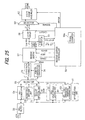
- Fig. 8 is a diagram showing the overall construction of an interface on the entrance side of an ATM network.
- An STS-3 line termination unit 10 receives STS-3 frame data from an OC3 transmission line, outputs a signal SPETOP at the timing of the reference position TOP (the position of the byte at row 1, column 10) of the cell conversion zone in the frame, and outputs the pointer POT and payload SPE of the AAL-1 cell conversion zone (the hatched portion) as frame data UPDAT.
- An AAL-1 cell generating unit 20 converts the entering frame data UPDAT into AAL-1 cells, incorporates the SDT pointer, which indicates the reference position TOP, into a prescribed AAL-1 cell and sends the cell to an ATM network.
- the AAL-1 cell generating unit 20 includes a signal creation unit (SSRTS) 21 for creating various signals such as an SDT pointer (PTR), a transmit signal RTS, an SC count value (SC) and a pointer-creation indication signal (PTREN); an SAR-PDU creation unit (SAAL1) 22 for creating an SAR-PDU header (PDUHDR) using the RTS information, SC count value and pointer-creation indication signal, etc.; a transmit-buffer write controller (SRWC) 23 for suitably selecting the SAR-PDU header (PDUHDR), SDT pointer (PTR) or frame data (UPDAT) and outputting the same as transmit-buffer write data (cell payload) SBWDAT; a transmit buffer (SBUF) 24, which comprises a FIFO buffer, for storing the 48-byte cell payload input thereto and successively outputting the same in response to a read-out request; a transmit-buffer read-out controller (SBRC) 25 for successively reading out and outputting the
- Fig. 9 is a diagram illustrating the construction of the signal generation unit 21 and Fig. 10 is a timing chart of the various signals.
- the reference-position signal SPETOP from the STS-3 line termination unit 10 and a master clock (byte timing pulse) UPCLK of the line on the upstream side enter the signal generation unit 21, and so does a 155.52-Mbps network clock, which is for RTS operation, that arrives from the ATM network.
- a payload-octet position creation unit 21b outputs the octet positions (0 ⁇ 46) of the SAR-PDU payload. More specifically, the payload-octet position creation unit 21b counts the byte timing pulses UPCLK (Fig. 10) in the AAl-1 cell conversion zone indicated by the bold border in Fig. 12 (namely when the STS-3 overhead indication signal RXOH is logical "0") and outputs the octet position (0 ⁇ 46) of the SAR-PDU payload as a signal OCTET. The payload-octet position creation unit 21b further outputs an SC enable signal (SCEN) whenever the numerical value OCTET becomes zero.
- SCEN SC enable signal
- a sequence count creation unit 21c counts the SC enable signal SCEN and outputs the sequence count (SC) of 0 ⁇ 7.
- An SDT pointer creation unit 21g has a downcounter DCNT for indicating each of 2358 byte positions in the AAL-1 cell conversion zone (the area enclosed by the border in Fig. 12) of the STS-3 frame.
- the downcounter DCNT (1) is preset to the numerical value 2357 by the reference-position signal SPETOP and (2) is decremented whenever the byte timing pulse UPCLK is generated in the AAl-1 cell conversion zone (namely when the STS-3 overhead indication signal RXOH is logical "0"), thereby outputting 2357 ⁇ 0 repetitively.
- a parity creation unit 21h creates even-numbered parity of the SDT pointer value.
- An 8-bit SDC pointer is constructed by the 7-bit SDT pointer value PTRV and 1-bit parity.
- Fig. 14 is a diagram illustrating the construction of the SAR-PDU header creation unit 22.
- a CRC creation unit 22b creates a 3-bit CRC in accordance with a predetermined CRC calculation equation using the SN field (CSI + SC), and a parity creation unit 23c creates even-numbered parity EPB for the seven bits of (CSI + SC + CRC).
- the SAR-PDU header creation unit 22 outputs CSI, SC, CRC and EPB as the SAR-PDU header (PDUHDR) cell by cell.
- Fig. 15 is a diagram showing the construction of the transmit-buffer write controller 23.
- a selector 23a suitably selects the SAR-PDU header (PDUHDR), SDT pointer PTR or STS-3 frame data UPDAT based upon the payload octet position signal OCTET and pointer-creation indication signal PTREN. As a result, the selector 23a sends transmit-buffer write data (cell payload) to the transmit buffer 24.
- a transmit-buffer write address creation unit 23b controls the generation of an address (SBWADR) for writing a cell payload to the transmit buffer and the generation of a write-enable signal (SBWEN).
- the transmit-buffer write address creation unit 23b regards this as transmit-buffer overflow and does not write data to the transmit buffer.
- Fig. 16 is a diagram showing the construction of the transmit buffer 24, which is constituted by an FIFO buffer and is capable of storing a maximum of four cells.
- a cell payload in the non-P-format is mapped to the transmit buffer in the manner shown in Fig. 17A, and cell payload data in the P-format is mapped to the transmit buffer in the manner shown in Fig. 17B.
- Fig. 18 is a diagram illustrating the construction of the transmit-buffer read-out controller 25.
- An ATM cell timing creation unit (53-octet counter) 25a drives the 53-octet counter by the highway clock within the switch and creates a 53-octet signal HTP that indicates the beginning of the ATM cell.
- a transmit-buffer read-out address creation unit 25b (1) generates a read-out address SBRADR for the transmit buffer 24 based upon the ATM cell timing, and (2) creates the transmit buffer full signal SBFULL and a transmit-buffer non-empty signal (reverse logic of transmit-buffer empty) *SBEMPTY based upon the write-completion signal SBWCOMP from the transmit-buffer write controller 23 and a read-out request SBRC from the ATM cell creation unit 26.
- the transmit buffer 24 is a FIFO buffer for a maximum of four cells, as mentioned above.
- the transmit-buffer read-out controller 25 monitors the amount of use of this buffer to thereby detect transmit-buffer overflow, inhibit the writing of data anew (i.e., discard data that the apparatus is attempting to write in) and notify of the occurrence of overflow.
- a pointer is used to manage the amount of buffer used.
- a write pointer (SBW_PTR) and a read-out pointer (SBR_PTR) are provided internally as the pointers. Both pointers can take on values of 0 to 3. The particular value indicates the logical address (in cell-payload units) of the transmit buffer.
- the trigger that advances the write pointer SBW PTR is entry of the write-completion signal SBWCOMP from the transmit-buffer write controller 23.
- the trigger that advances the read-out pointer SBR PTA is entry of the read-out request SBRC from the ATM cell creation unit 26; this is the time at which read-out processing is completed.
- there are two buffer states namely transmit-buffer empty SBEMPTY and transmit-buffer full SBFULL, which indicate that the transfer buffer is empty and full, respectively, when their logic values are "1".
- the transmit-buffer read-out address creation unit 25b manages the amount of transmit-buffer use as follows:
- Fig. 19 is a diagram showing the construction of the ATM cell creation unit 26.
- a read-out request generator 26a sends the read-out request SBRC to the transmit-buffer read-out controller 25 when the transmit buffer 24 is not empty.
- An ATM-header application timing creation unit 26b outputs a header selection signal HSL based upon the signal HTP indicating the beginning of the ATM cell.
- a selector 26c selects and outputs the ATM cell header if header selection signal HSL is "1" and selects and outputs transmit-buffer read-out data (the cell payload) at all other timings.
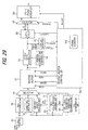
- Fig. 20 is a diagram showing the overall construction of an interface on the exit side of an ATM network.
- a cell filter 50 subjects cells that enter from an ATM highway to filtering based upon VPI/VCI values and selects/passes cells that it itself is to process.
- a cell determination unit 51 has a cell valid/invalid judging unit 52 and a cell loss / erroneous insertion examining unit 53.
- the cell valid/invalid judging unit 52 checks the SN/SNP field of the SAR-PDU header of each individual cell that has passed through the cell filter 50, i.e., performs a CRC check and parity check concerning each cell and judges the normality of the SAR-PDU header information.
- a 1-bit error of the CRC is capable of being corrected and is corrected.
- the result of the cell valid/invalid judgment is "valid" or "invalid” and is reported to the cell loss / erroneous insertion examining unit 53.
- An "invalid" judgment means that an SAR-
- the cell loss / erroneous insertion examining unit 53 checks for loss and erroneous insertion of cells based upon the judgment made by the cell valid/invalid judging unit 52 and the continuity of the sequence count SC in the SN field and, on the basis of the check, decides to load a received cell into a receive buffer 57 or to discard the cell or, if cell loss has been determined, to insert a dummy cell.
- SN check algorithm sequence-number check algorithm
- a cell accumulator 54 stores temporarily a cell which the cell loss / erroneous insertion examining unit 53 is currently examining to determine whether or not it should be introduced to the receive buffer. If the cell loss / erroneous insertion examining unit 53 has decided that cell loss has occurred, a dummy cell creation unit 55 creates and outputs the data of the dummy cell that corresponds to the lost cell. On the basis of the decision made by the cell loss / erroneous insertion examining unit 53 to load a cell, discard a cell or insert a dummy cell, a selector 56 selects and outputs a cell from the cell accumulator 54 or a dummy cell from the dummy cell creation unit 55. Further, the selector 56 divides a 48-byte cell payload into 12 bytes four times in parallel fashion and assembles these bytes as shown in Fig. 21A, whereupon the payload is input to the receive buffer 57.
- the receive buffer 57 is a play-out buffer provided for two purposes, namely (1) for clock transfer and (2) to accommodate fluctuations in cell arrival.
- the receive buffer 57 has a capacity for storing a prescribed number of cell payloads (SAR-PDU header + 47-byte information).
- a receive-buffer controller 58 outputs a write-enable signal WREN, a write address signal WRADD, a read-out-enable signal DREN, a read-out address signal RDADD, a latch-enable signal LATCHEN, a select signal RDPHASE and the reference-position signal SPETOP. More specifically, the receive-buffer controller 58 holds the write address signal WRADD, generates the write-enable signal WREN whenever data is output from the selector 56, synchronizes this data to the write clock, writes this data to the receive buffer 57 and increments the write address signal WRADD. As long as the receive buffer 57 is not empty, data is read out of the receive buffer continuously in sync with the read-out clock.
- a pointer detector 61 detects the SDT pointer PTR from the two high-order bits of the payload read out of the receive buffer 57 and inputs a pointer value and a pointer-detection signal PTR-DET to the receive-buffer controller 58.
- the latter is internally provided with a frame counter 58a that counts from 0 to 2429 for the purpose of counting 2430 bytes of an STS-3 frame.
- the frame counter 58a is preset to [2429 - pointer value] when a pointer is detected and then starts counting up at the byte timing.
- the receive-buffer controller 58 outputs the reference-position signal SPETOP at the time at which counted value becomes equal to 9, namely at the timing of the frame reference position TOP (the starting position of the AAL-1 cell conversion zone).
- the receive-buffer controller 58 outputs the select signal RDPHASE, which specifies which byte output from the latch circuit 59 is to be delivered as an output. More specifically, depending upon whether or not the pointer-detection signal PTR-DET has been applied thereto, the receive-buffer controller 58 determines whether data that has been read out of the receive buffer 57 is the cell payload of a P-format cell or the cell payload of a non-P-format cell. In addition,
- the selector sends the user data indicated by the hatching in Fig. 21B to the STS-3 frame assembler 62 at the byte timing of the AAL cell conversion zone and outputs dummy data in the overhead interval.
- the STS-3 frame assembler 62 assembles the user data, which enters from the selector 60 at the byte timing of the AAL cell conversion zone, into the STS-3 frame format, creates the section overhead SH and line overhead LH at the overhead byte timing, embeds the created overhead in the overhead field to complete the STS frame data and then sends this data to the STS-3 transmission line.
- the data that has been read out of the receive buffer 57 is subjected to a band adjustment.
- the band adjustment prevents loss of a large quantity of reproduced data due to loss of a P-format cell and prevents the initial fill level (IFL) of the receive buffer from fluctuating.
- Fig. 22 is a diagram showing the construction of an interface provided on the exit side of an ATM network and having a band adjustment function. Components identical with those shown in Fig. 20 are designated by like reference characters. This arrangement differs in that (1) an SAR-PDU header creation unit 71 is provided; (2) the cell determination unit 51 outputs a cell-header valid/invalid determination signal INV and a dummy-cell data insertion signal DUM; and (3) the pointer detector 61 is replaced by a pointer detector / P-format cell detector 72.
- the cell valid/invalid judging unit 52 subjects each individual cell that has passed through the cell filter 50 to a CRC check and parity check, judges the normality of the SAR-PDU header information and outputs the cell-header valid/invalid determination signal INV.
- the cell loss / erroneous insertion examining unit 53 checks for loss and erroneous insertion of cells based upon the judgment made by the cell valid/invalid judging unit 52 and the continuity of the sequence count SC in the SN field and, on the basis of the check, decides to load a received cell into the receive buffer 57 or to discard the cell or, if cell loss has been determined, to insert a dummy cell.
- the dummy insertion signal DUM in which "0" indicates "normal” and "1" indicates "dummy insertion" is output.
- the SAR-PDU header creation unit 71 creates the SAR-PDU header shown in Fig. 23 using CSI, SC contained in the SAR-PDU header that enters from the cell filter 50 as well as the cell-header valid/invalid determination signal INV and dummy insertion signal DUM that enter from the cell determination unit 51.
- the selector 56 selects and outputs, 12 bytes at a time, the total of one byte of SAR-PDU data that has been created by the SAR-PDU header creation unit 71 and 47-byte cell-payload data from the second byte onward that has been stored in the cell accumulator 54 (see Fig. 23).
- the selector 56 selects and outputs, 12 bytes at a time, the total of one byte of SAR-PDU data that has been created by the SAR-PDU header creation unit 71 and 47-byte dummy data that has been generated by the dummy cell creation unit 55.
- the pointer detector / P-format cell detector 72 is internally provided with a downcounter SPECTR that counts from 2357 to 0 to indicate 2358 byte positions (see Fig. 12) of the AAL-1 cell conversion zone.
- the downcounter SPECTR is preset to the pointer value at the time of pointer detection, after which the downcounter counts down cyclically at the byte timing of the AAL-1 cell conversion zone.
- the pointer detector / P-format cell detector 72 executes pointer-detection / P-format determination processing, which is illustrated in Fig. 24, and outputs (1) the SDT pointer value (PTR value) and pointer-detection signal PTR-DET and (2) outputs a P-format cell determination signal PFORM.
- the P-format cell detection signal ARDYPFMT is a signal that is reset to "0" at the beginning of one cycle of SC values 0 to 7; at detection of a P-format cell, the signal takes on the "1" level until it is reset.
- VALIDPTR is a pointer detection signal that rises to logical "1" when a true SDT pointer has been detected, and NPORP is a signal that rises to logical "1" when a P-format cell has been detected.
- a cell (a dummy cell for which the SC value is even or an invalid cell for which the SC value is even) that has a high likelihood of being a P-format cell is assumed to be a P-format cell when a P-format cell has been lost. Furthermore, pointer timing is predicted using the value of the count recorded by the downcounter SPECTR. When a P-format cell has been lost at the predicted timing, a dummy cell or invalid cell for which the SC value is even at this timing is judged to be a P-format cell. As a result, judgment of P-format cells can be made with greater precision.
- the cell valid/invalid judging unit 52, cell loss / erroneous insertion examining unit 53, cell accumulator 54, dummy cell creation unit 55, selector 56 and SAR-PDU header creation unit 71 operate in the same manner as set forth in connection with the first embodiment of Fig. 20.
- the selector 56 splits, 12 bytes at a time four times, the total of one byte of SAR-PDU data that has been created by the SAR-PDU header creation unit 71 and 47-byte cell-payload data from the second byte onward that has been stored in the cell accumulator 54, and outputs the result (see Fig. 23).
- the selector 56 splits, 12 bytes at a time four times, the total of one byte of SAR-PDU data that has been created by the SAR-PDU header creation unit 71 and 47-byte dummy data that has been created by the dummy cell creation unit 55, and outputs the result.
- the data accumulator 73 stores a payload of one cycle output from the selector 56, and the pointer correction controller 74 performs pointer correction, in accordance with the flowchart of pointer correction processing shown in Fig. 26, while referring to the SAR-PDU header of each cell of one cycle of accumulated cells.
- the data accumulator 73 receives and accumulates a cell payload output from the selector 56 (step 201).
- the CSI of the SAR-PDU header that is the first byte of the cell payload is made "1" and the pointer value that is the second byte is made 127 (indicative of a false pointer) (step 207).
- a cell that has been corrected by the above-described processing is stored in the receive buffer 57, after which control similar to that of the embodiment shown in Fig. 20 is carried out and user data is sent from the receive buffer 57 to the STS-3 frame assembler 62.
- a cell (a dummy cell for which the SC value is even or an invalid cell for which the SC value is even) that has a high likelihood of being a P-format cell is assumed to be a P-format cell when a P-format cell has been lost.
- Fig. 27 is a diagram showing another construction of an interface provided on the exit side of an ATM network and having a band adjustment function. Components identical with those shown in Fig. 25 are designated by like reference characters. This arrangement differs in that (1) a data accumulator 75 for one cell is provided in front of the receive buffer 57, and (2) a pointer correction controller 76 for correcting a pointer in accordance with the flowchart of Fig. 28 upon referring successively to the SAR-PDU headers of cells is provided in front of the receive buffer 57.
- the data accumulator for one cycle employed in the second embodiment may be dispensed with, thereby making it possible to assume that a cell is a P-format cell through a simpler arrangement.
- processing can be simplified over that of the second embodiment by taking into consideration the fact that the content of STS-3 frame data cannot be reproduced normally in such case. Moreover, coincidence of the bands corresponding to both the STS-3 and ATM networks can be assured.
- Fig. 29 is a diagram showing the construction of a fourth embodiment of an interface provided on the exit side of an ATM network and having a band adjustment function. Components identical with those shown in Fig. 25 are designated by like reference characters.
- This arrangement differs in that the data accumulator 73 for one cycle and pointer correction controller 74 are provided on the output side (read-out side) of the receive buffer 57. This is the difference between whether pointer correction control is performed before a cell payload is written to the receive buffer (the second embodiment) and whether pointer correction control is performed after a cell payload is read out of the receive buffer (the third embodiment). The way in which pointer correction control is performed, however is the same.
- data accumulator 75 and pointer correction controller 76 in the third embodiment can similarly be provided on the read-out side of the receive buffer 57.
- the fourth embodiment provides effects similar to those of the third embodiment.
- the necessary part of overhead and payload are adopted as a cell conversion zone, whereby transmission band can be reduced.
- a pointer specifying the reference position (e.g., starting position) of the cell conversion zone is included in a cell, the original frame format can be assembled from received cells.
- a P-format cell if a P-format cell is lost owing to cell loss or cell garbling, etc., a P-format cell can be generated, it can be so arranged that the IFL set for a receive buffer will not fluctuate, and it can be so arranged that starvation and overflow will not occur.
- a cell (a dummy cell for which the SC value is even or an invalid cell for which the SC value is even) that has a high likelihood of being a P-format cell is assumed to be a P-format cell when a P-format cell has been lost.
- the fact that a prescribed cell is assumed to be a P-format cell assures that a large quantity of reproduced data will not be lost as a consequence of loss of P-format cells.
- pointer timing is predicted using the value of a count recorded by a downcounter SPECTR.
- a P-format cell is lost at the predicted timing, a prescribed cell is judged to be a P-format cell based upon this timing.
- SC 0 ⁇ 7
- the IFL of a receive buffer can be prevented from fluctuating as a result of judging a P-format cell to be a non-P-format cell or judging a non-P-format cell to be a P-format cell.
- the fact that a prescribed cell is assumed to be a P-format cell assures that a large quantity of reproduced data will not be lost as a consequence of loss of P-format cells.
- a dummy cell for which the SC value is even or an invalid cell for which the SC value is even at this timing is judged to be a P-format cell. This makes it possible to raise the precision with which P-format cells are judged.
Landscapes
- Engineering & Computer Science (AREA)
- Computer Networks & Wireless Communication (AREA)
- Signal Processing (AREA)
- Data Exchanges In Wide-Area Networks (AREA)
Applications Claiming Priority (2)
| Application Number | Priority Date | Filing Date | Title |
|---|---|---|---|
| JP2000117886 | 2000-04-19 | ||
| JP2000117886A JP3782283B2 (ja) | 2000-04-19 | 2000-04-19 | インタフェース装置 |
Publications (2)
| Publication Number | Publication Date |
|---|---|
| EP1148757A2 true EP1148757A2 (fr) | 2001-10-24 |
| EP1148757A3 EP1148757A3 (fr) | 2004-04-07 |
Family
ID=18629128
Family Applications (1)
| Application Number | Title | Priority Date | Filing Date |
|---|---|---|---|
| EP01101163A Withdrawn EP1148757A3 (fr) | 2000-04-19 | 2001-01-23 | Appareil d'interface |
Country Status (3)
| Country | Link |
|---|---|
| US (1) | US6826192B2 (fr) |
| EP (1) | EP1148757A3 (fr) |
| JP (1) | JP3782283B2 (fr) |
Families Citing this family (24)
| Publication number | Priority date | Publication date | Assignee | Title |
|---|---|---|---|---|
| GB0110437D0 (en) * | 2001-04-27 | 2001-06-20 | Marconi Comm Ltd | A transmission method |
| US7133415B2 (en) * | 2001-07-10 | 2006-11-07 | Corrigent Systems Ltd. | SONET circuit emulation with VT compression |
| JP4165044B2 (ja) * | 2001-07-23 | 2008-10-15 | 沖電気工業株式会社 | セル分解装置 |
| US7103049B2 (en) * | 2002-01-02 | 2006-09-05 | Adtran, Inc. | Mechanism for providing octet alignment in serial ATM data stream |
| US7844697B1 (en) * | 2002-01-25 | 2010-11-30 | Juniper Networks, Inc. | Measuring network traffic based on predicted amount of padding |
| DE10235921A1 (de) * | 2002-03-25 | 2003-10-09 | Agere Syst Guardian Corp | Verfahren und Vorrichtung zum Verbessern der Zuverlässigkeit von mittels konkreter Syntaxschreibweise codierten Nachrichten |
| US7894480B1 (en) * | 2002-08-27 | 2011-02-22 | Hewlett-Packard Company | Computer system and network interface with hardware based rule checking for embedded firewall |
| US7474672B2 (en) * | 2003-02-11 | 2009-01-06 | International Business Machines Corporation | Frame alteration logic for network processors |
| US7515605B2 (en) * | 2003-03-24 | 2009-04-07 | Corrigent Systems Ltd | Efficient transport of TDM services over packet networks |
| US7835397B2 (en) * | 2003-04-25 | 2010-11-16 | Alcatel-Lucent Usa Inc. | Frame processing |
| US7386010B2 (en) * | 2003-06-13 | 2008-06-10 | Corrigent Systems Ltd | Multiprotocol media conversion |
| US7974223B2 (en) | 2004-11-19 | 2011-07-05 | Corrigent Systems Ltd. | Virtual private LAN service over ring networks |
| US7515536B2 (en) * | 2005-07-11 | 2009-04-07 | Corrigent Systems Ltd. | Transparent transport of fibre channel traffic over packet-switched networks |
| US7983150B2 (en) * | 2006-01-18 | 2011-07-19 | Corrigent Systems Ltd. | VPLS failure protection in ring networks |
| US7808931B2 (en) * | 2006-03-02 | 2010-10-05 | Corrigent Systems Ltd. | High capacity ring communication network |
| US20070242676A1 (en) * | 2006-04-13 | 2007-10-18 | Corrigent Systems Ltd. | Interface between a synchronous network and high-speed ethernet |
| US7593400B2 (en) * | 2006-05-19 | 2009-09-22 | Corrigent Systems Ltd. | MAC address learning in a distributed bridge |
| US7660303B2 (en) | 2006-08-22 | 2010-02-09 | Corrigent Systems Ltd. | Point-to-multipoint functionality in a bridged network |
| US9451338B2 (en) * | 2006-10-13 | 2016-09-20 | Lantiq Beteiligungs-GmbH & Co. KG | Line card with network processing device and data pump device |
| GB2466046A (en) * | 2008-12-09 | 2010-06-16 | Polar Extreme Res Ltd | Generalised self-referential file system using unique identifiers for data transfer |
| US8345680B2 (en) * | 2009-05-07 | 2013-01-01 | Alcatel Lucent | Handling out-of-sequence packets in a circuit emulation service |
| JP5896433B2 (ja) * | 2011-06-24 | 2016-03-30 | ▲ホア▼▲ウェイ▼技術有限公司Huawei Technologies Co.,Ltd. | 管理ユニット−3回路のためのエミュレーション方法および装置 |
| US8995263B2 (en) * | 2012-05-22 | 2015-03-31 | Marvell World Trade Ltd. | Method and apparatus for internal/external memory packet and byte counting |
| US9131010B2 (en) * | 2012-10-19 | 2015-09-08 | Nec Laboratories America, Inc. | Delay-tolerant and loss-tolerant data transfer for mobile applications |
Family Cites Families (8)
| Publication number | Priority date | Publication date | Assignee | Title |
|---|---|---|---|---|
| JPH0498943A (ja) | 1990-08-17 | 1992-03-31 | Hitachi Ltd | 非同期転送モードを用いたバーチャルコンテナの伝送方法及び回路 |
| JPH06169320A (ja) | 1992-10-02 | 1994-06-14 | Toshiba Corp | Atmセル化装置 |
| EP0649234B1 (fr) | 1993-10-14 | 2001-09-19 | International Business Machines Corporation | Procédé et dispositif pour transférer des données dans un réseau à ATM |
| GB2291561B (en) | 1994-05-21 | 1998-09-23 | Northern Telecom Ltd | Communications system |
| JP3357973B2 (ja) | 1996-03-08 | 2002-12-16 | 株式会社日立製作所 | Aal1処理方法とその装置 |
| JP2817699B2 (ja) | 1996-03-13 | 1998-10-30 | 日本電気株式会社 | Stm−atm変換装置 |
| JP3185922B2 (ja) * | 1998-04-16 | 2001-07-11 | 日本電気株式会社 | 2重化構成aal終端装置および同期化方法 |
| JP3635926B2 (ja) * | 1998-05-14 | 2005-04-06 | Kddi株式会社 | 網接続装置 |
-
2000
- 2000-04-19 JP JP2000117886A patent/JP3782283B2/ja not_active Expired - Fee Related
-
2001
- 2001-01-19 US US09/766,001 patent/US6826192B2/en not_active Expired - Lifetime
- 2001-01-23 EP EP01101163A patent/EP1148757A3/fr not_active Withdrawn
Also Published As
| Publication number | Publication date |
|---|---|
| US6826192B2 (en) | 2004-11-30 |
| JP2001308863A (ja) | 2001-11-02 |
| JP3782283B2 (ja) | 2006-06-07 |
| US20010033575A1 (en) | 2001-10-25 |
| EP1148757A3 (fr) | 2004-04-07 |
Similar Documents
| Publication | Publication Date | Title |
|---|---|---|
| US6826192B2 (en) | Interface apparatus | |
| US5559959A (en) | Method for transmitting message cells via redundant virtual path pairs of an atm communication network | |
| JP2948464B2 (ja) | 非同期転送モード(atm)ペイロード同期装置 | |
| US6034954A (en) | Multiplexing apparatus for transit of signals between service provided by low-speed transmission path and ATM service provided by high-speed transmission path | |
| JP3630460B2 (ja) | データ長補正システム | |
| CA2132063A1 (fr) | Methode et circuit pour transmettre des cellules de message via des paires de trajets virtuels redondants dans un reseau de communication mta | |
| EP0866631A2 (fr) | Dispositif de terminaison de plusieurs lignes et son procédé "OAM" | |
| EP0909105B1 (fr) | Dispositif de multiplexage de cellules courtes | |
| US20050180331A1 (en) | ATM cell transfer apparatus with hardware structure for OAM cell generation | |
| JPH0614049A (ja) | Atmにおけるセル廃棄制御装置及びその方法 | |
| JP3245333B2 (ja) | Cbr信号の位相跳躍防止方式 | |
| US6628659B1 (en) | ATM cell switching system | |
| EP1225732B1 (fr) | Procedé et dipsositif pour attribuer des unités de données de cellules à des positions sequentiels de stockage en utilisant une estimation de la position du pointeur | |
| US6292487B1 (en) | Data transmission system and method | |
| EP1111827A2 (fr) | STS-n à granularité améliorée | |
| WO2000059261A1 (fr) | Structure de trame de mini-cellules aal2 sur une structure de canal nx64 kbps e1/t1 | |
| US7167477B2 (en) | Apparatus and method for recovering abnormal control cells in asynchronous transfer mode exchange subscriber unit | |
| EP0757503A2 (fr) | Dispositif et procédé pour la mise en oeuvre des fonctions de protocol de la couche d'adaptation ATM (AAL1) dans un réseau de communication à large bande | |
| JP2685082B2 (ja) | Stm信号とatm信号の変換/逆変換方式 | |
| JP3618095B2 (ja) | ショートセル分離装置 | |
| JPH0955752A (ja) | 2重化stm/atm変換装置の同期化方法 | |
| US7224694B2 (en) | Apparatus for and method of generating pointers for transfer of structured data in AAL1 | |
| US8009679B2 (en) | Communication system and method | |
| JP3536790B2 (ja) | Aal1信号伝送による導通確認システム及びその方法 | |
| EP1946498B1 (fr) | Systeme et procede de communication |
Legal Events
| Date | Code | Title | Description |
|---|---|---|---|
| PUAI | Public reference made under article 153(3) epc to a published international application that has entered the european phase |
Free format text: ORIGINAL CODE: 0009012 |
|
| AK | Designated contracting states |
Kind code of ref document: A2 Designated state(s): AT BE CH CY DE DK ES FI FR GB GR IE IT LI LU MC NL PT SE TR |
|
| AX | Request for extension of the european patent |
Free format text: AL;LT;LV;MK;RO;SI |
|
| PUAL | Search report despatched |
Free format text: ORIGINAL CODE: 0009013 |
|
| AK | Designated contracting states |
Kind code of ref document: A3 Designated state(s): AT BE CH CY DE DK ES FI FR GB GR IE IT LI LU MC NL PT SE TR |
|
| AX | Request for extension of the european patent |
Extension state: AL LT LV MK RO SI |
|
| AKX | Designation fees paid | ||
| REG | Reference to a national code |
Ref country code: DE Ref legal event code: 8566 |
|
| STAA | Information on the status of an ep patent application or granted ep patent |
Free format text: STATUS: THE APPLICATION IS DEEMED TO BE WITHDRAWN |
|
| 18D | Application deemed to be withdrawn |
Effective date: 20041008 |