EP1150355A1 - Microcircuit integre, circuit integre, carte a circuits imprimes et dispositif electronique - Google Patents
Microcircuit integre, circuit integre, carte a circuits imprimes et dispositif electronique Download PDFInfo
- Publication number
- EP1150355A1 EP1150355A1 EP99972788A EP99972788A EP1150355A1 EP 1150355 A1 EP1150355 A1 EP 1150355A1 EP 99972788 A EP99972788 A EP 99972788A EP 99972788 A EP99972788 A EP 99972788A EP 1150355 A1 EP1150355 A1 EP 1150355A1
- Authority
- EP
- European Patent Office
- Prior art keywords
- input
- output terminals
- integrated circuit
- terminals
- substrate
- Prior art date
- Legal status (The legal status is an assumption and is not a legal conclusion. Google has not performed a legal analysis and makes no representation as to the accuracy of the status listed.)
- Withdrawn
Links
Images





Classifications
-
- H—ELECTRICITY
- H10—SEMICONDUCTOR DEVICES; ELECTRIC SOLID-STATE DEVICES NOT OTHERWISE PROVIDED FOR
- H10P—GENERIC PROCESSES OR APPARATUS FOR THE MANUFACTURE OR TREATMENT OF DEVICES COVERED BY CLASS H10
- H10P74/00—Testing or measuring during manufacture or treatment of wafers, substrates or devices
- H10P74/27—Structural arrangements therefor
- H10P74/273—Interconnections for measuring or testing, e.g. probe pads
-
- H—ELECTRICITY
- H10—SEMICONDUCTOR DEVICES; ELECTRIC SOLID-STATE DEVICES NOT OTHERWISE PROVIDED FOR
- H10D—INORGANIC ELECTRIC SEMICONDUCTOR DEVICES
- H10D89/00—Aspects of integrated devices not covered by groups H10D84/00 - H10D88/00
- H10D89/10—Integrated device layouts
-
- H—ELECTRICITY
- H10—SEMICONDUCTOR DEVICES; ELECTRIC SOLID-STATE DEVICES NOT OTHERWISE PROVIDED FOR
- H10W—GENERIC PACKAGES, INTERCONNECTIONS, CONNECTORS OR OTHER CONSTRUCTIONAL DETAILS OF DEVICES COVERED BY CLASS H10
- H10W72/00—Interconnections or connectors in packages
- H10W72/50—Bond wires
- H10W72/541—Dispositions of bond wires
- H10W72/5449—Dispositions of bond wires not being orthogonal to a side surface of the chip, e.g. fan-out arrangements
-
- H—ELECTRICITY
- H10—SEMICONDUCTOR DEVICES; ELECTRIC SOLID-STATE DEVICES NOT OTHERWISE PROVIDED FOR
- H10W—GENERIC PACKAGES, INTERCONNECTIONS, CONNECTORS OR OTHER CONSTRUCTIONAL DETAILS OF DEVICES COVERED BY CLASS H10
- H10W90/00—Package configurations
- H10W90/701—Package configurations characterised by the relative positions of pads or connectors relative to package parts
- H10W90/751—Package configurations characterised by the relative positions of pads or connectors relative to package parts of bond wires
- H10W90/756—Package configurations characterised by the relative positions of pads or connectors relative to package parts of bond wires between a chip and a stacked lead frame, conducting package substrate or heat sink
Definitions
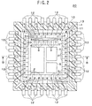
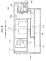
- the integrated circuit element 20 comprises the chip 10, an island 11 for mounting the chip thereon, leads 12 and a package 13 of a resin for encapsulating these elements therein.
- the leads 12 are each connected to the bonding pads 3 of the I/O terminals 2 by wires 14, respectively.
- a semiconductor wafer is used as the substrate 1 and a semiconductor fabricating techniques such as film formation, diffusion and/or photolithography are employed to form the circuit modules 6, 7 and 8 and the I/O terminals 2 and 4 on the substrate 1. Then, the semiconductor wafer is diced to obtain the substrate 1 having a size of a ⁇ b. Thus, the chip 10 is provided.
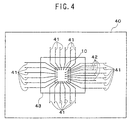
- the semiconductor wafer before dicing or the chip 10 after the dicing may be placed at a central portion of the opening 43 of the probe card 40 to contact the probes 41 and 42 with the bonding pad 3 and the pad for probing, respectively, for allowing signals to be inputted or outputted from or to an external circuit through the probes 41 and 42.
- the operation test of the circuit modules 6, 7 and 8 and the checking of the fabrication conditions, i.e. whether the film forming or etching is being carried out as designed can be effected.
- the chip 10 is so constructed that the I/O terminals are divided into the I/O terminals 2 for users and the I/O terminals 4 for testing, and only the I/O terminals 2 are arranged around the periphery of the chip 10.
- This construction allows the chip size to be reduced as compared with conventional chips in which all the I/O terminals are arranged around the periphery of the chip.
- the number of the I/O terminals which should be bonded is reduced, and therefore the time necessary for bonding can also be reduced. Thus, the fabrication efficiency can be improved.
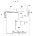
- the chip 10 is mounted on the printed circuit board 50 in the form of the packaged integrated circuit element 20 in the foregoing embodiments, the chip 10 may be directly bonded on the printed circuit board 50. In this case, the mounting efficiency is further enhanced because the package is not needed. This realizes a more small-sized printed circuit board 50 or electronic device 100. Further, the cost can be more lowered due to the fact that the package is not needed and there can be provided the printed circuit board 50 and the electronic device 100 of a lower price.
Landscapes
- Semiconductor Integrated Circuits (AREA)
- Tests Of Electronic Circuits (AREA)
- Lead Frames For Integrated Circuits (AREA)
Applications Claiming Priority (3)
| Application Number | Priority Date | Filing Date | Title |
|---|---|---|---|
| JP33138498 | 1998-11-20 | ||
| JP33138498 | 1998-11-20 | ||
| PCT/JP1999/006480 WO2000031799A1 (fr) | 1998-11-20 | 1999-11-19 | Microcircuit integre, circuit integre, carte a circuits imprimes et dispositif electronique |
Publications (2)
| Publication Number | Publication Date |
|---|---|
| EP1150355A1 true EP1150355A1 (fr) | 2001-10-31 |
| EP1150355A4 EP1150355A4 (fr) | 2003-09-10 |
Family
ID=18243096
Family Applications (1)
| Application Number | Title | Priority Date | Filing Date |
|---|---|---|---|
| EP99972788A Withdrawn EP1150355A4 (fr) | 1998-11-20 | 1999-11-19 | Microcircuit integre, circuit integre, carte a circuits imprimes et dispositif electronique |
Country Status (10)
| Country | Link |
|---|---|
| US (2) | US6469396B1 (fr) |
| EP (1) | EP1150355A4 (fr) |
| KR (1) | KR20010080509A (fr) |
| CN (1) | CN1155089C (fr) |
| AU (1) | AU1184400A (fr) |
| BR (1) | BR9915509A (fr) |
| CA (1) | CA2351417A1 (fr) |
| HK (1) | HK1041102A1 (fr) |
| TW (1) | TW442945B (fr) |
| WO (1) | WO2000031799A1 (fr) |
Cited By (2)
| Publication number | Priority date | Publication date | Assignee | Title |
|---|---|---|---|---|
| EP1376693A3 (fr) * | 2002-05-28 | 2006-12-27 | NEC Electronics Corporation | Dispositif semi-conductrice de type puce enversée avec de modules E/S dans une region de circuit interne |
| EP2421041A4 (fr) * | 2009-04-15 | 2013-06-26 | Olympus Medical Systems Corp | Dispositif semi-conducteur et procédé de fabrication d'un dispositif semi-conducteur |
Families Citing this family (19)
| Publication number | Priority date | Publication date | Assignee | Title |
|---|---|---|---|---|
| DE10123758B4 (de) * | 2001-05-16 | 2008-04-03 | Texas Instruments Deutschland Gmbh | Multi-Chip-Modul mit mehreren integrierten Halbleiterschaltungen |
| JP2003098221A (ja) * | 2001-09-25 | 2003-04-03 | Mitsubishi Electric Corp | 半導体装置、半導体装置の試験方法及び半導体装置の試験装置 |
| US6781218B1 (en) * | 2003-03-04 | 2004-08-24 | Nptest, Inc. | Method and apparatus for accessing internal nodes of an integrated circuit using IC package substrate |
| WO2004104607A1 (fr) * | 2003-05-21 | 2004-12-02 | Advantest Corporation | Appareil de test et module de test |
| US7214886B2 (en) * | 2003-11-25 | 2007-05-08 | International Business Machines Corporation | High performance chip carrier substrate |
| US20050248028A1 (en) * | 2004-05-05 | 2005-11-10 | Cheng-Yen Huang | Chip-packaging with bonding options connected to a package substrate |
| EP1610384A3 (fr) * | 2004-06-14 | 2008-11-19 | Denso Corporation | Unité életctronique avec un substrat où un circuit électronique est fabriqué |
| CN100464413C (zh) * | 2004-12-24 | 2009-02-25 | 北京中星微电子有限公司 | 实现芯片管脚功能互换的电路及芯片 |
| JP5264135B2 (ja) * | 2006-11-09 | 2013-08-14 | パナソニック株式会社 | 半導体集積回路及びマルチチップモジュール |
| US8197055B2 (en) * | 2006-11-29 | 2012-06-12 | Seiko Epson Corporation | Patterning method, droplet discharging device and circuit board |
| JP5141121B2 (ja) * | 2006-11-29 | 2013-02-13 | セイコーエプソン株式会社 | パターン形成方法、液滴吐出装置及び回路基板 |
| CN101206179B (zh) * | 2006-12-22 | 2010-08-11 | 中芯国际集成电路制造(上海)有限公司 | 光发射显微镜样品 |
| KR101224426B1 (ko) * | 2007-12-28 | 2013-01-22 | 후지쯔 세미컨덕터 가부시키가이샤 | 반도체 장치 및 그 제조 방법 |
| JP5239766B2 (ja) * | 2008-11-14 | 2013-07-17 | 富士通セミコンダクター株式会社 | レイアウト設計方法 |
| KR101097247B1 (ko) * | 2009-10-26 | 2011-12-21 | 삼성에스디아이 주식회사 | 전자 회로 모듈 및 그 제조 방법 |
| TW201134317A (en) * | 2010-03-29 | 2011-10-01 | Hon Hai Prec Ind Co Ltd | Pins assignment for circuit board |
| US9500700B1 (en) * | 2013-11-15 | 2016-11-22 | Xilinx, Inc. | Circuits for and methods of testing the operation of an input/output port |
| TWI639847B (zh) * | 2017-06-27 | 2018-11-01 | Powerchip Technology Corporation | 積體電路晶片及其檢查方法 |
| JP6400795B1 (ja) * | 2017-06-29 | 2018-10-03 | タイコエレクトロニクスジャパン合同会社 | 印刷回路基板 |
Family Cites Families (18)
| Publication number | Priority date | Publication date | Assignee | Title |
|---|---|---|---|---|
| US3905094A (en) * | 1972-01-10 | 1975-09-16 | Displaytek Corp | Thermal display module |
| US4220917A (en) * | 1978-07-31 | 1980-09-02 | International Business Machines Corporation | Test circuitry for module interconnection network |
| US4386389A (en) * | 1981-09-08 | 1983-05-31 | Mostek Corporation | Single layer burn-in tape for integrated circuit |
| JPS58161336A (ja) * | 1982-03-19 | 1983-09-24 | Hitachi Ltd | 半導体集積回路装置 |
| JPS6262552A (ja) | 1985-09-12 | 1987-03-19 | Nec Corp | 大規模集積回路 |
| JPS63244853A (ja) * | 1987-03-31 | 1988-10-12 | Nec Corp | 半導体集積回路装置 |
| JPS63310155A (ja) * | 1987-06-12 | 1988-12-19 | Seiko Instr & Electronics Ltd | 半導体集積回路装置 |
| JPH01198051A (ja) | 1988-02-03 | 1989-08-09 | Tokyo Electron Ltd | 半導体集積回路 |
| JP2901156B2 (ja) * | 1990-08-31 | 1999-06-07 | 三菱電機株式会社 | 半導体集積回路装置 |
| JPH05198637A (ja) * | 1992-01-23 | 1993-08-06 | Mitsubishi Electric Corp | 半導体集積回路及びそのテスト方法 |
| US5453991A (en) * | 1992-03-18 | 1995-09-26 | Kabushiki Kaisha Toshiba | Integrated circuit device with internal inspection circuitry |
| JPH07122701A (ja) | 1993-10-21 | 1995-05-12 | Hitachi Ltd | 半導体装置およびその製造方法ならびにpga用リードフレーム |
| US5969538A (en) * | 1996-10-31 | 1999-10-19 | Texas Instruments Incorporated | Semiconductor wafer with interconnect between dies for testing and a process of testing |
| JP3565991B2 (ja) * | 1996-06-26 | 2004-09-15 | 株式会社ルネサステクノロジ | 半導体集積回路および半導体集積回路の製造方法 |
| TW432669B (en) * | 1997-04-25 | 2001-05-01 | Sharp Kk | Semiconductor integrated circuit device capable of achieving reductions in chip area and consumption power |
| JP2998702B2 (ja) | 1997-06-13 | 2000-01-11 | 日本電気株式会社 | 半導体集積回路 |
| JP4014708B2 (ja) * | 1997-08-21 | 2007-11-28 | 株式会社ルネサステクノロジ | 半導体集積回路装置の設計方法 |
| JP2001274323A (ja) * | 2000-03-24 | 2001-10-05 | Hitachi Ltd | 半導体装置とそれを搭載した半導体モジュール、および半導体装置の製造方法 |
-
1999
- 1999-11-15 TW TW088119880A patent/TW442945B/zh not_active IP Right Cessation
- 1999-11-18 US US09/442,700 patent/US6469396B1/en not_active Expired - Lifetime
- 1999-11-19 WO PCT/JP1999/006480 patent/WO2000031799A1/fr not_active Ceased
- 1999-11-19 AU AU11844/00A patent/AU1184400A/en not_active Abandoned
- 1999-11-19 KR KR1020017006338A patent/KR20010080509A/ko not_active Withdrawn
- 1999-11-19 HK HK02101860.3A patent/HK1041102A1/en unknown
- 1999-11-19 CA CA002351417A patent/CA2351417A1/fr not_active Abandoned
- 1999-11-19 BR BR9915509-5A patent/BR9915509A/pt not_active Application Discontinuation
- 1999-11-19 CN CNB998135275A patent/CN1155089C/zh not_active Expired - Lifetime
- 1999-11-19 EP EP99972788A patent/EP1150355A4/fr not_active Withdrawn
-
2002
- 2002-06-24 US US10/178,110 patent/US6548910B2/en not_active Expired - Lifetime
Cited By (2)
| Publication number | Priority date | Publication date | Assignee | Title |
|---|---|---|---|---|
| EP1376693A3 (fr) * | 2002-05-28 | 2006-12-27 | NEC Electronics Corporation | Dispositif semi-conductrice de type puce enversée avec de modules E/S dans une region de circuit interne |
| EP2421041A4 (fr) * | 2009-04-15 | 2013-06-26 | Olympus Medical Systems Corp | Dispositif semi-conducteur et procédé de fabrication d'un dispositif semi-conducteur |
Also Published As
| Publication number | Publication date |
|---|---|
| US6469396B1 (en) | 2002-10-22 |
| CN1155089C (zh) | 2004-06-23 |
| CA2351417A1 (fr) | 2000-06-02 |
| TW442945B (en) | 2001-06-23 |
| BR9915509A (pt) | 2001-11-13 |
| AU1184400A (en) | 2000-06-13 |
| US6548910B2 (en) | 2003-04-15 |
| CN1326592A (zh) | 2001-12-12 |
| WO2000031799A1 (fr) | 2000-06-02 |
| HK1041102A1 (en) | 2002-06-28 |
| US20020153538A1 (en) | 2002-10-24 |
| EP1150355A4 (fr) | 2003-09-10 |
| KR20010080509A (ko) | 2001-08-22 |
Similar Documents
| Publication | Publication Date | Title |
|---|---|---|
| US6548910B2 (en) | Integrated circuit element, printed circuit board and electronic device having input/output terminals for testing and operation | |
| US6218202B1 (en) | Semiconductor device testing and burn-in methodology | |
| KR100616055B1 (ko) | 메모리 모듈 및 그 제조 방법 | |
| US8647976B2 (en) | Semiconductor package having test pads on top and bottom substrate surfaces and method of testing same | |
| US6380615B1 (en) | Chip size stack package, memory module having the same, and method of fabricating the module | |
| US8115321B2 (en) | Separate probe and bond regions of an integrated circuit | |
| JP2005322921A (ja) | バンプテストのためのフリップチップ半導体パッケージ及びその製造方法 | |
| US7238962B2 (en) | Semiconductor chip with test pads and tape carrier package using the same | |
| JP5594661B2 (ja) | 半導体装置 | |
| WO2006098364A1 (fr) | Carte de modules | |
| JP5218319B2 (ja) | 半導体基板 | |
| US7868439B2 (en) | Chip package and substrate thereof | |
| JP4539396B2 (ja) | 半導体装置の実装構造 | |
| JPWO2000031799A1 (ja) | 集積回路チップ、集積回路素子、プリント回路基板、電子機器 | |
| CN119252813B (zh) | 封装结构以及芯片 | |
| KR100665843B1 (ko) | 반도체 장치에서의 패드 배치 구조 및 방법 | |
| KR100378185B1 (ko) | 테스트용 탭을 구비하는 마이크로 비지에이 패키지 테이프 | |
| JP5626232B2 (ja) | 半導体装置 | |
| JP4056252B2 (ja) | 半導体装置の製造方法 | |
| JP2561005B2 (ja) | 半導体装置 | |
| MXPA01005000A (en) | Integrated circuit plate, integrated circuit, printed circuit board and electron device | |
| JPH04373131A (ja) | 高密度実装用icペレット | |
| JP2007281011A (ja) | アナログ・デジタル混載半導体装置 | |
| JP4388989B2 (ja) | 半導体チップマウント封止サブ基板 | |
| JPH06101500B2 (ja) | 半導体集積回路装置 |
Legal Events
| Date | Code | Title | Description |
|---|---|---|---|
| PUAI | Public reference made under article 153(3) epc to a published international application that has entered the european phase |
Free format text: ORIGINAL CODE: 0009012 |
|
| 17P | Request for examination filed |
Effective date: 20010618 |
|
| AK | Designated contracting states |
Kind code of ref document: A1 Designated state(s): AT BE CH CY DE DK ES FI FR GB GR IE IT LI LU MC NL PT SE |
|
| A4 | Supplementary search report drawn up and despatched |
Effective date: 20030729 |
|
| 17Q | First examination report despatched |
Effective date: 20031105 |
|
| STAA | Information on the status of an ep patent application or granted ep patent |
Free format text: STATUS: THE APPLICATION IS DEEMED TO BE WITHDRAWN |
|
| 18D | Application deemed to be withdrawn |
Effective date: 20041201 |
|
| REG | Reference to a national code |
Ref country code: HK Ref legal event code: WD Ref document number: 1041102 Country of ref document: HK |