EP1155452B1 - Halbleiteranordnung mit sicherheitsbeschichtung und chipkarte mit einer solchen anordnung - Google Patents
Halbleiteranordnung mit sicherheitsbeschichtung und chipkarte mit einer solchen anordnung Download PDFInfo
- Publication number
- EP1155452B1 EP1155452B1 EP00979619A EP00979619A EP1155452B1 EP 1155452 B1 EP1155452 B1 EP 1155452B1 EP 00979619 A EP00979619 A EP 00979619A EP 00979619 A EP00979619 A EP 00979619A EP 1155452 B1 EP1155452 B1 EP 1155452B1
- Authority
- EP
- European Patent Office
- Prior art keywords
- coating
- semiconductor device
- filler
- security
- matrix
- Prior art date
- Legal status (The legal status is an assumption and is not a legal conclusion. Google has not performed a legal analysis and makes no representation as to the accuracy of the status listed.)
- Expired - Lifetime
Links
Images

Classifications
-
- H—ELECTRICITY
- H10—SEMICONDUCTOR DEVICES; ELECTRIC SOLID-STATE DEVICES NOT OTHERWISE PROVIDED FOR
- H10W—GENERIC PACKAGES, INTERCONNECTIONS, CONNECTORS OR OTHER CONSTRUCTIONAL DETAILS OF DEVICES COVERED BY CLASS H10
- H10W42/00—Arrangements for protection of devices
- H10W42/40—Arrangements for protection of devices protecting against tampering, e.g. unauthorised inspection or reverse engineering
-
- Y—GENERAL TAGGING OF NEW TECHNOLOGICAL DEVELOPMENTS; GENERAL TAGGING OF CROSS-SECTIONAL TECHNOLOGIES SPANNING OVER SEVERAL SECTIONS OF THE IPC; TECHNICAL SUBJECTS COVERED BY FORMER USPC CROSS-REFERENCE ART COLLECTIONS [XRACs] AND DIGESTS
- Y10—TECHNICAL SUBJECTS COVERED BY FORMER USPC
- Y10T—TECHNICAL SUBJECTS COVERED BY FORMER US CLASSIFICATION
- Y10T428/00—Stock material or miscellaneous articles
- Y10T428/26—Web or sheet containing structurally defined element or component, the element or component having a specified physical dimension
Definitions
- the invention relates to a semiconductor device having a substrate on a first side of which there are provided a first semiconductor element and at least one security coating which comprises a powdery filler incorporated in a matrix.
- the invention also relates to a smartcard provided with a semiconductor device comprising a memory and a security coating which comprises a powdery first filler incorporated in a matrix.
- US-A 5,399,441 discloses a semiconductor device of the type mentioned in the opening paragraph wherein the security coating is a layer having a matrix of silicon oxide in which a powdery filler is incorporated.
- the security coating is a layer having a matrix of silicon oxide in which a powdery filler is incorporated.
- the matrix is filled with a filler, such as an oxide, a nitride or a carbide of silicon, aluminum or a metal
- the coating inhibits at least 90% of the transmission of visible light.
- the matrix is filled with an inorganic salt of a heavy metal, the coating inhibits at least 90% of the transmission of a specific type of infrared radiation.
- a first object of the invention to provide a semiconductor device of the type mentioned in the opening paragraph wherein the coating inhibits transmission of visible light and of near infrared radiation to a larger extent. It is a second object to provide a smart card of the type mentioned in the opening paragraph whose semiconductor device has such an improved coating.
- the first object is achieved in that:
- the second filler is a material, for example, in the form of particles which transforms incident radiation into heat. With this material, the coating absorbs the radiation for at least 99 per cent. The coating with the second filler absorbs the radiation to at least 1400 nm. Radiation of a wavelength larger than 1.4 ⁇ m need not be absorbed as much as 99%, as the large wavelength itself hides details of the first semiconductor element in the semiconductor device of the invention. Preferably, the coating with the second filler absorbs the radiation of wavelengths in the range of from 800 to 2000 nm. Suitable materials are, for instance, titanium nitride and titanium oxynitride.
- the second filler in a preferred embodiment comprises titanium nitride. Due to the use of titanium nitride as a second filler, the transmittance of at least 99.9 % of radiation of a wavelength of between 600 and 2000 nm can be easily inhibited.
- the inventors have found that particles of TiN in the coating can have a surface comprising TiO 2 , which is believed to follow from accidental oxidation. Such oxidation occurs, for example, when the security coating is applied during the manufacture of the semiconductor device from an acid, aqueous composition.
- a first advantage of this second filler is that titanium nitride is known to be used in the manufacture of semiconductor devices in cleanroom facilities. Moreover, it is free of heavy metals. This is an important advantage as heavy metals are poisonous materials that present problems both during the production and as waste after disposal of the semiconductor device comprising the security coating. A further advantage is that titanium nitride is commercially available in various particle sizes.
- the first filler present in the security coating of the device of the invention operates by scattering visible light. Radiation in the visible spectrum as well as in the ultraviolet spectrum is thus inhibited from penetrating by scattered reflection. In order to ensure that the coating has sufficient scattering potential, it was found that the difference between the refractive index of the first filler and that of the matrix should at least be 0.3. As the refractive index of a matrix is generally of the order of 1.4-1.5, first fillers with a refractive index larger than 1.7-1.8 can be used.
- first fillers examples include oxides of zirconium, titanium, zinc, manganese, chromium, niobium, iron, nickel, strontium, yttrium, vanadium, gallium, copper and cobalt and nitrides of niobium, titanium and zirconium.
- the first filler in a further embodiment comprises titanium oxide.
- This material has a very high refractive index and causes, therefore, intense scattering of visible light and of radiation in the ultraviolet spectrum.
- titanium nitride is used as the second filler, it is preferred to have a weight ratio of titanium oxide and titanium nitride in the range of from 0.25 to 4 in the coating.
- the amount of filler used in the coating of the semiconductor device of the present invention can be varied over a wide range, depending, for example, on the electrical characteristics desired in the coating.
- the first and the second filler are present in a combined amount in the range of from 10 to 90 per cent by weight of the coating.
- the first and the second filler are preferably present as particles of a size in the submicron range.
- the material of the matrix of the coating can be chosen from several materials, such as a mono(metal)phosphate compound wherein the metal is, for example, chosen from the group of zinc and aluminum, or a component prepared from a silica precursor resin.
- a mono(metal)phosphate compound wherein the metal is, for example, chosen from the group of zinc and aluminum, or a component prepared from a silica precursor resin.
- matrices are described, for example, in the non-prepublished application WO IB99/01007 and in US-A 5,399,441.
- monoaluminum phosphate is used for the matrix.
- the security coating has a great mechanical strength and a good etching persistency.
- the coating with monoaluminum phosphate can be readily provided in a thickness ranging from 1 to 10 ⁇ m.
- the coating has a thickness in the range of from1 to 5 ⁇ m. It is especially preferred to have a coating thickness of less than 3 ⁇ m.
- the coating is nevertheless opaque to visible light and near infrared radiation.
- a first advantage is that the thickness of the semiconductor device is only slightly increased by the provision of the security coating. This is advantageous for the use of the semiconductor device of the invention in a smartcard in which the device thickness is limited.
- a second advantage is that it is also possible to apply more than one coating in the semiconductor device.
- a third advantage is that the application of end-contacts in the manufacture of the semiconductor device is easier than in the case of coatings of larger thickness.
- end-contacts can be applied by way of a method successively comprising the steps of depositing a photoresist in regions where end-contacts are desired; depositing and drying a composition comprising fillers incorporated in a matrix; removing the photoresist and the composition deposited thereon; heating so as to form the security coating; and applying an electrically suitably conducting material, such as copper, in said regions.
- a coating thickness of less than 5 ⁇ m facilitates the removal of the photoresist and the coating deposited thereon.
- ком ⁇ онент which modifies the surface of the fillers for better adhesion or a dispersion agent may be used.
- a further embodiment of the semiconductor device of the invention comprises a light-sensitive element which is covered by the security coating and, after damaging of the security coating, reacts to exposure to visible light by inducing a permanent change of state of the element containing data to be protected.
- Said reaction taking place in this embodiment after malicious damaging of the coating, can be of an electrical or chemical nature.
- the layout of selected parts of the semiconductor device, such as a layer comprising interconnect lines, is thus destroyed.
- Another embodiment of the semiconductor device of the invention comprises a light-sensitive element and an electrically programmable element containing data to be protected, which elements are covered by the security coating and which light-sensitive element, after damaging of the coating, reacts to exposure to visible light by inducing erasure of the data to be protected and by bringing the electrically programmable element into a non-programmable state.
- Said light-sensitive elements comprise, for example, resistors in combination with diodes or transistors which are coupled to an output terminal, such as an amplifier.
- An example of a light-sensitive element is known for EP-A 0939 933. It comprises a biasing transistor arranged to provide a bias current, a reverse biased transistor with a control electrode arranged to be reverse biased by said bias current and with a conducting electrode, and also a resistor coupled between a supply voltage and said conducting electrode. Incident visible light is detected by a voltage drop at the conducting electrode of the reverse biased transistor which can then apply a signal to the output.
- the output can induce the resetting of an electrically erasable programmable random-access memory known as EEPROM.
- the output can also induce complete writing of a one-time electrically programmable random-access memory. The complete writing causes erasure of the data to be protected.
- the substrate of the semiconductor device of the invention can be made from several materials. Suitable materials are, for example, silica, alumina and a polymer material such as polyimide. There are several materials and constructions which can be used in the first semiconductor element of the semiconductor device of the invention. Known constructions are, for example, the MOS field effect transistor and the bipolar transistor. Such a construction can comprises memory units as is known per se. Known materials comprise metals, inorganic semiconductors and organic conductors and semiconductors.
- the semiconductor device constitutes a vital part of a smart card, such as a cash card, a credit card or any other card.
- a smart card such as a cash card, a credit card or any other card.
- the expression "smart card” is meant to describe in general any portable apparatus which comprises a semiconductor device that contains only data which cannot be changed by the apparatus alone.
- the smart card is a card-like apparatus, at present, the introduction of contactless smartcards makes it possible to incorporate the function of the smart card into other apparatus such as, for example, an electronic diary.
- the second object of the invention is achieved in that if the smart cardcomprises the semiconductor device of the invention. It is thus protected against visual inspection from outside.
- the smart card comprises the semiconductor device of the invention provided with a light-sensitive element so as to protect the memory of the smart card against visual inspection after opening of the semiconductor device.
- the semiconductor device 20 in Figure 1 has a substrate 1 of silica with a first side 2.
- a first semiconductor element 3 which is, in this example, a bipolar transistor with an emitter region 4, a base region 5 and a collector region 6.
- Said regions 4,5 and 6 are provided in a first layer 7 which is covered with a patterned insulating layer 8 of silicon oxide.
- the insulating layer 8 is patterned such that it has contact windows 9 and 10 wherethrough a patterned conductive layer 11 of aluminum contacts the emitter region 4 and the base region 5.
- a passivation layer 13 is provided on the first side 2. This passivation layer 13 is for example a layer of silicon oxide or silicon nitride.
- the first side 2 is also provided with a security coating 14 according to the invention. Both the passivation layer 13 and the security coating 14 leave the conductive layer 11 exposed in the region 12, thus forming a contact face so as to enable external contact.
- the passivation layer 13 has been patterned according to a known method. Subsequently, a photoresist has been deposited onto the passivation layer 13 at desired regions. These regions comprise, for example, the region 12 and regions in which the semiconductor device 20 is separated from a neighboring device manufactured from the same slice of silicon. Such regions are commonly referred to as scribe lines.
- a composition was prepared to spincoat on the passivation layer 13 of the substrate 1 of the semiconductor device 20.
- the composition comprised 50 grams of monoaluminum phosphate acidified with 50 grams of 0.01 M hydrochloric acid, a hydrolysis mixture of tetraethoxysilane (TEOS) comprising 5 grams of TEOS, 25 grams of TiO 2 and 25 grams of TiN.
- TEOS tetraethoxysilane
- the coating liquid was spincoated on the passivation layer 13 and on the conductive layer 11 which was covered by a photostructured polymer on contact faces and on sawlines.
- the coating 14 thus formed was dried at 100°C and the photoresist was removed by means of ethanol.
- the monoaluminum phosphate matrix was formed next by heating the layer at a temperature in the range of from 400 to 500°.
- the first semiconductor element 3 is shown, but in practice the first layer 7 generally comprises a plurality of such elements and the conductive layer 11 comprises a number of layers and, in addition, is provided with many connection faces for external contact.
- the assembly may form an integrated circuit.
- field effect transistors can be present instead of or in addition to the bipolar transistor.
- other elements such as capacitors, resistors and diodes, can also be integrated in the semiconductor device 20.
- a security coating 14 in accordance with the invention is provided on the passivation layer 13.
- the matrix of the coating 14 comprises molecules of a first material, in this case monoaluminum phosphate Al(OPO 3 H 2 ) 3 , which molecules are bonded to the surface of the passivation layer and to each other. The bonds are formed by condensation of hydroxyl groups.
- Figure 2 shows the molecules of the matrix and the particles which act as the first or the second filler in a transition state to bonding. In this state the coating has an internal structure as in the bonded state, but no condensation has taken place yet.
- the matrix also comprises particles of TiO 2 en TiN which act as the first and the second filler in the matrix.
- the particles preferably have an average particle size of between 50 nm and 1 ⁇ m.
- the TiN-particles have a oxidized surface, e.g. their surface mainly comprises TiO 2 , and they can be bonded to the matrix as easily as the TiO 2 -particles.
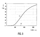
- Figure 3 shows the transmission T in % of radiation by two different security coatings A and B as a function of the wavelength ⁇ between 400 and 2000 nm.
- the first coating A not being in conformity with the invention, consisted of about 55 weight per cent of monoaluminum phosphate, about 40 weight per cent of particles of TiO 2 as the first filler and about 5 weight per cent of tetraethoxysiloxane.
- the coating A had a thickness of 4 ⁇ m. Whereas the transmission is very low in the range from 400 to 600 nm, the transmission increases up to 50 per cent at about 1300 nm and to 75 per cent at about 2000 nm.
- the second line shows the transmission by a security coating according to the invention, consisting of about 48 weight per cent monoaluminum phosphate, about 24 weight per cent of particles of TiO 2 , about 24 weight per cent of particles of TiN and about 4 weight per cent of tetraethoxysiloxane.
- a security coating consisting of about 48 weight per cent monoaluminum phosphate, about 24 weight per cent of particles of TiO 2 , about 24 weight per cent of particles of TiN and about 4 weight per cent of tetraethoxysiloxane.
- the transmission is inhibited in the spectrum from 400 to 2000 nm for a very large part, e.g. for more than 99.99 per cent. Therefore, the invention provides an excellent security coating which certainly improves the known security coating and with which data can be protected very well.
Landscapes
- Semiconductor Integrated Circuits (AREA)
- Structures Or Materials For Encapsulating Or Coating Semiconductor Devices Or Solid State Devices (AREA)
Claims (8)
- Halbleiteranordnung (20) mit einem Substrat (1), wobei auf einer ersten Seite (2) davon ein erstes Halbleiterelement (3) und mindestens eine Sicherheitsbeschichtung (14), die einen pulverförmigen, in eine Matrix eingearbeiteten Füllstoff umfasst, aufgebracht sind, dadurch gekennzeichnet, dass- der Unterschied zwischen dem Brechungsindex des pulverförmigen ersten Füllstoffs und dem der Matrix mindestens 0,3 ist, und- die Beschichtung einen zweiten Füllstoff so umfasst, dass die Beschichtung ein erheblicher Absorber von Strahlung ist, der Strahlung mit Wellenlängen mindestens in dem Bereich von 800 bis 1400 nm um mindestens 99 % absorbiert und worin der zweite Füllstoff frei von Schwermetallen ist.
- Halbleiteranordnung (20) nach Anspruch 1, dadurch gekennzeichnet, dass der zweite Füllstoff TiN umfasst.
- Halbleiteranordnung (20) nach Anspruch 1 oder 2, dadurch gekennzeichnet, dass der erste Füllstoff TiO2 umfasst.
- Halbleiteranordnung (20) nach Anspruch 1, dadurch gekennzeichnet, dass die Matrix der Sicherheitsbeschichtung Monoaluminiumphosphat umfasst.
- Halbleiteranordnung (20) nach Anspruch 4, dadurch gekennzeichnet, dass die Sicherheitsbeschichtung eine Dicke von weniger als 3 µm hat.
- Halbleiteranordnung (20) nach Anspruch 1, dadurch gekennzeichnet, dass sie ein lichtempfindliches Element und ein Element, das Daten enthält, beinhaltet, wobei die Elemente durch die Sicherheitsbeschichtung (14) bedeckt sind und wobei das lichtempfindliche Element nach Beschädigung der Beschichtung darauf reagiert, dass es sichtbarem Licht ausgesetzt ist, indem es eine permanente Veränderung des Zustands des Elements, das Daten enthält, bewirkt.
- Halbleiteranordnung (20) nach Anspruch 1, dadurch gekennzeichnet, dass sie ein lichtempfindliches Element und ein elektrisch programmierbares Element, das Daten enthält, beinhaltet, wobei die Elemente durch die Sicherheitsbeschichtung (14) bedeckt sind und wobei das lichtempfindliche Element nach Beschädigung der Beschichtung darauf reagiert, dass es sichtbarem Licht ausgesetzt ist, indem es Löschen der Daten bewirkt und das elektrisch programmierbare Element in einen nicht-programmierbaren Zustand bringt.
- Chipkarte, die mit der Halbleiteranordnung (20) nach einem der Ansprüche 1 bis 7 versehen ist.
Priority Applications (1)
| Application Number | Priority Date | Filing Date | Title |
|---|---|---|---|
| EP00979619A EP1155452B1 (de) | 1999-12-09 | 2000-11-22 | Halbleiteranordnung mit sicherheitsbeschichtung und chipkarte mit einer solchen anordnung |
Applications Claiming Priority (4)
| Application Number | Priority Date | Filing Date | Title |
|---|---|---|---|
| EP99204177 | 1999-12-09 | ||
| EP99204177 | 1999-12-09 | ||
| PCT/EP2000/011657 WO2001043191A1 (en) | 1999-12-09 | 2000-11-22 | Semiconductor device comprising a security coating and smartcard provided with such a device |
| EP00979619A EP1155452B1 (de) | 1999-12-09 | 2000-11-22 | Halbleiteranordnung mit sicherheitsbeschichtung und chipkarte mit einer solchen anordnung |
Publications (2)
| Publication Number | Publication Date |
|---|---|
| EP1155452A1 EP1155452A1 (de) | 2001-11-21 |
| EP1155452B1 true EP1155452B1 (de) | 2006-10-18 |
Family
ID=8240978
Family Applications (1)
| Application Number | Title | Priority Date | Filing Date |
|---|---|---|---|
| EP00979619A Expired - Lifetime EP1155452B1 (de) | 1999-12-09 | 2000-11-22 | Halbleiteranordnung mit sicherheitsbeschichtung und chipkarte mit einer solchen anordnung |
Country Status (6)
| Country | Link |
|---|---|
| US (1) | US6759736B2 (de) |
| EP (1) | EP1155452B1 (de) |
| JP (1) | JP2003516575A (de) |
| DE (1) | DE60031375T2 (de) |
| TW (1) | TW502286B (de) |
| WO (1) | WO2001043191A1 (de) |
Families Citing this family (36)
| Publication number | Priority date | Publication date | Assignee | Title |
|---|---|---|---|---|
| US6968686B2 (en) * | 2001-07-11 | 2005-11-29 | Hideaki Okada | Operation mechanism of a variable displacement hydraulic pump |
| US6798693B2 (en) | 2001-09-18 | 2004-09-28 | Kilopass Technologies, Inc. | Semiconductor memory cell and memory array using a breakdown phenomena in an ultra-thin dielectric |
| JP4599059B2 (ja) | 2001-09-18 | 2010-12-15 | キロパス テクノロジー インコーポレイテッド | 超薄膜誘電体のブレークダウン現象を利用した半導体メモリセルセル及びメモリアレイ |
| US6700151B2 (en) * | 2001-10-17 | 2004-03-02 | Kilopass Technologies, Inc. | Reprogrammable non-volatile memory using a breakdown phenomena in an ultra-thin dielectric |
| US6766960B2 (en) * | 2001-10-17 | 2004-07-27 | Kilopass Technologies, Inc. | Smart card having memory using a breakdown phenomena in an ultra-thin dielectric |
| US6898116B2 (en) | 2002-04-26 | 2005-05-24 | Kilopass Technologies, Inc. | High density semiconductor memory cell and memory array using a single transistor having a buried N+ connection |
| US6940751B2 (en) * | 2002-04-26 | 2005-09-06 | Kilopass Technologies, Inc. | High density semiconductor memory cell and memory array using a single transistor and having variable gate oxide breakdown |
| US6777757B2 (en) | 2002-04-26 | 2004-08-17 | Kilopass Technologies, Inc. | High density semiconductor memory cell and memory array using a single transistor |
| US6992925B2 (en) | 2002-04-26 | 2006-01-31 | Kilopass Technologies, Inc. | High density semiconductor memory cell and memory array using a single transistor and having counter-doped poly and buried diffusion wordline |
| IL165468A0 (en) | 2002-06-04 | 2006-01-15 | Nds Ltd | Prevention of tampering in electronic devices |
| US7042772B2 (en) * | 2002-09-26 | 2006-05-09 | Kilopass Technology, Inc. | Methods and circuits for programming of a semiconductor memory cell and memory array using a breakdown phenomenon in an ultra-thin dielectric |
| US7031209B2 (en) * | 2002-09-26 | 2006-04-18 | Kilopass Technology, Inc. | Methods and circuits for testing programmability of a semiconductor memory cell and memory array using a breakdown phenomenon in an ultra-thin dielectric |
| US6791891B1 (en) | 2003-04-02 | 2004-09-14 | Kilopass Technologies, Inc. | Method of testing the thin oxide of a semiconductor memory cell that uses breakdown voltage |
| US6924664B2 (en) * | 2003-08-15 | 2005-08-02 | Kilopass Technologies, Inc. | Field programmable gate array |
| US6972986B2 (en) * | 2004-02-03 | 2005-12-06 | Kilopass Technologies, Inc. | Combination field programmable gate array allowing dynamic reprogrammability and non-votatile programmability based upon transistor gate oxide breakdown |
| US7064973B2 (en) * | 2004-02-03 | 2006-06-20 | Klp International, Ltd. | Combination field programmable gate array allowing dynamic reprogrammability |
| DE102004015546B4 (de) * | 2004-03-30 | 2011-05-12 | Infineon Technologies Ag | Halbleiterchip mit integrierter Schaltung und Verfahren zum Sichern einer integrierten Halbleiterschaltung |
| US20050218929A1 (en) * | 2004-04-02 | 2005-10-06 | Man Wang | Field programmable gate array logic cell and its derivatives |
| US7755162B2 (en) | 2004-05-06 | 2010-07-13 | Sidense Corp. | Anti-fuse memory cell |
| US8735297B2 (en) | 2004-05-06 | 2014-05-27 | Sidense Corporation | Reverse optical proximity correction method |
| JP4981661B2 (ja) | 2004-05-06 | 2012-07-25 | サイデンス コーポレーション | 分割チャネルアンチヒューズアレイ構造 |
| US9123572B2 (en) | 2004-05-06 | 2015-09-01 | Sidense Corporation | Anti-fuse memory cell |
| US7164290B2 (en) * | 2004-06-10 | 2007-01-16 | Klp International, Ltd. | Field programmable gate array logic unit and its cluster |
| US20050275427A1 (en) * | 2004-06-10 | 2005-12-15 | Man Wang | Field programmable gate array logic unit and its cluster |
| FR2872610B1 (fr) * | 2004-07-02 | 2007-06-08 | Commissariat Energie Atomique | Dispositif de securisation de composants |
| US7135886B2 (en) * | 2004-09-20 | 2006-11-14 | Klp International, Ltd. | Field programmable gate arrays using both volatile and nonvolatile memory cell properties and their control |
| US7193436B2 (en) * | 2005-04-18 | 2007-03-20 | Klp International Ltd. | Fast processing path using field programmable gate array logic units |
| US7482925B2 (en) * | 2005-06-24 | 2009-01-27 | Visa U.S.A. | Apparatus and method to electromagnetically shield portable consumer devices |
| FR2893183B1 (fr) * | 2005-11-10 | 2008-01-25 | Gemplus Sa | Procede de protection d'un composant electronique contre les attaques par injection de faute |
| US20080128022A1 (en) * | 2006-11-15 | 2008-06-05 | First Solar, Inc. | Photovoltaic device including a tin oxide protective layer |
| US8505826B2 (en) * | 2007-04-16 | 2013-08-13 | Visa U.S.A. | Anti-interrogation for portable device |
| US8604995B2 (en) * | 2007-06-11 | 2013-12-10 | Visa U.S.A. Inc. | Shielding of portable consumer device |
| US20100234209A1 (en) * | 2007-10-16 | 2010-09-16 | Nxp B.V. | Particle comprising core and shell and applications thereof |
| US8038068B2 (en) | 2007-11-28 | 2011-10-18 | Visa U.S.A. Inc. | Multifunction removable cover for portable payment device |
| JP6405556B2 (ja) * | 2013-07-31 | 2018-10-17 | リンテック株式会社 | 保護膜形成フィルム、保護膜形成用シートおよび検査方法 |
| US10559505B2 (en) * | 2014-01-22 | 2020-02-11 | Lintec Corporation | Protective film-forming film, sheet for forming protective film, complex sheet for forming protective film, and inspection method |
Family Cites Families (13)
| Publication number | Priority date | Publication date | Assignee | Title |
|---|---|---|---|---|
| US4243427A (en) * | 1977-11-21 | 1981-01-06 | Trw Inc. | High concentration phosphoro-silica spin-on dopant |
| US5053992A (en) * | 1990-10-04 | 1991-10-01 | General Instrument Corporation | Prevention of inspection of secret data stored in encapsulated integrated circuit chip |
| US5258334A (en) * | 1993-01-15 | 1993-11-02 | The U.S. Government As Represented By The Director, National Security Agency | Process of preventing visual access to a semiconductor device by applying an opaque ceramic coating to integrated circuit devices |
| US5387480A (en) * | 1993-03-08 | 1995-02-07 | Dow Corning Corporation | High dielectric constant coatings |
| US5591680A (en) * | 1993-12-06 | 1997-01-07 | Micron Communications | Formation methods of opaque or translucent films |
| US5399441A (en) * | 1994-04-12 | 1995-03-21 | Dow Corning Corporation | Method of applying opaque coatings |
| US5693701A (en) * | 1995-10-26 | 1997-12-02 | Dow Corning Corporation | Tamper-proof electronic coatings |
| US5711987A (en) * | 1996-10-04 | 1998-01-27 | Dow Corning Corporation | Electronic coatings |
| US5730792A (en) * | 1996-10-04 | 1998-03-24 | Dow Corning Corporation | Opaque ceramic coatings |
| US5892661A (en) * | 1996-10-31 | 1999-04-06 | Motorola, Inc. | Smartcard and method of making |
| GB2319602B (en) | 1996-11-21 | 2000-10-04 | Motorola Ltd | Light detection device |
| EP1029347B1 (de) * | 1998-06-10 | 2007-02-07 | Koninklijke Philips Electronics N.V. | Halbleiteranordnung mit einer integrierten schaltung und keramischer sicherheitsschicht und verfahren zum herstellen solcher anordnung |
| US20020033486A1 (en) * | 2000-08-04 | 2002-03-21 | Samsung Electronics Co., Ltd. | Method for forming an interconnection line using a hydrosilsesquioxane (HSQ) layer as an interlayer insulating layer |
-
2000
- 2000-11-02 TW TW089123103A patent/TW502286B/zh not_active IP Right Cessation
- 2000-11-22 DE DE60031375T patent/DE60031375T2/de not_active Expired - Lifetime
- 2000-11-22 EP EP00979619A patent/EP1155452B1/de not_active Expired - Lifetime
- 2000-11-22 JP JP2001543779A patent/JP2003516575A/ja not_active Withdrawn
- 2000-11-22 WO PCT/EP2000/011657 patent/WO2001043191A1/en not_active Ceased
- 2000-12-06 US US09/730,656 patent/US6759736B2/en not_active Expired - Lifetime
Also Published As
| Publication number | Publication date |
|---|---|
| EP1155452A1 (de) | 2001-11-21 |
| US20010003374A1 (en) | 2001-06-14 |
| DE60031375T2 (de) | 2007-09-20 |
| DE60031375D1 (de) | 2006-11-30 |
| TW502286B (en) | 2002-09-11 |
| US6759736B2 (en) | 2004-07-06 |
| WO2001043191A1 (en) | 2001-06-14 |
| JP2003516575A (ja) | 2003-05-13 |
Similar Documents
| Publication | Publication Date | Title |
|---|---|---|
| EP1155452B1 (de) | Halbleiteranordnung mit sicherheitsbeschichtung und chipkarte mit einer solchen anordnung | |
| CN101772775B (zh) | 抗篡改半导体器件以及制造该抗篡改半导体器件的方法 | |
| US8581251B2 (en) | Device for protecting an electronic integrated circuit housing against physical or chemical ingression | |
| US7696625B2 (en) | Semiconductor device and method for manufacturing the same | |
| US6198155B1 (en) | Semiconductor device comprising an integrated circuit provided with a ceramic security coating and method of manufacturing such a device | |
| CN1134825C (zh) | 安全半导体器件 | |
| US20080042226A1 (en) | Surface-shape sensor and method of manufacturing the same | |
| DE102016109960B4 (de) | Halbleitergehäuse, Chipkarte und Verfahren zum Herstellen eines Halbleitergehäuses | |
| JP2520857B2 (ja) | 集積半導体回路 | |
| US20070222043A1 (en) | Semiconductor device and a method of manufacturing the same | |
| CN100431140C (zh) | 具有保护性安全涂层的半导体器件及其制造方法 | |
| RU2419873C2 (ru) | Документ с электронным прибором | |
| JP4386570B2 (ja) | 安全集積回路デバイスとその製造方法 | |
| US20070085225A1 (en) | Encapsulation of a chip module | |
| JPH11504164A (ja) | チップカバー | |
| JPH10270605A (ja) | 半導体装置 | |
| WO1996016445A1 (en) | Integrated circuit structure with security feature | |
| JP2000112825A (ja) | 半導体装置 | |
| KR100480451B1 (ko) | 소자 보호용 층을 갖는 반도체 소자 | |
| JPH10270583A (ja) | 半導体装置 | |
| CA2195602A1 (en) | Method of protecting light sensitive regions of integrated circuits |
Legal Events
| Date | Code | Title | Description |
|---|---|---|---|
| PUAI | Public reference made under article 153(3) epc to a published international application that has entered the european phase |
Free format text: ORIGINAL CODE: 0009012 |
|
| AK | Designated contracting states |
Kind code of ref document: A1 Designated state(s): AT BE CH CY DE DK ES FI FR GB GR IE IT LI LU MC NL PT SE TR |
|
| AX | Request for extension of the european patent |
Free format text: AL;LT;LV;MK;RO;SI |
|
| 17P | Request for examination filed |
Effective date: 20011214 |
|
| RBV | Designated contracting states (corrected) |
Designated state(s): DE FR GB |
|
| 17Q | First examination report despatched |
Effective date: 20050427 |
|
| GRAP | Despatch of communication of intention to grant a patent |
Free format text: ORIGINAL CODE: EPIDOSNIGR1 |
|
| GRAS | Grant fee paid |
Free format text: ORIGINAL CODE: EPIDOSNIGR3 |
|
| GRAA | (expected) grant |
Free format text: ORIGINAL CODE: 0009210 |
|
| AK | Designated contracting states |
Kind code of ref document: B1 Designated state(s): DE FR GB |
|
| REG | Reference to a national code |
Ref country code: GB Ref legal event code: FG4D |
|
| REF | Corresponds to: |
Ref document number: 60031375 Country of ref document: DE Date of ref document: 20061130 Kind code of ref document: P |
|
| REG | Reference to a national code |
Ref country code: GB Ref legal event code: 732E |
|
| REG | Reference to a national code |
Ref country code: FR Ref legal event code: TP |
|
| ET | Fr: translation filed | ||
| PLBE | No opposition filed within time limit |
Free format text: ORIGINAL CODE: 0009261 |
|
| STAA | Information on the status of an ep patent application or granted ep patent |
Free format text: STATUS: NO OPPOSITION FILED WITHIN TIME LIMIT |
|
| 26N | No opposition filed |
Effective date: 20070719 |
|
| PGFP | Annual fee paid to national office [announced via postgrant information from national office to epo] |
Ref country code: DE Payment date: 20091119 Year of fee payment: 10 |
|
| PGFP | Annual fee paid to national office [announced via postgrant information from national office to epo] |
Ref country code: GB Payment date: 20091118 Year of fee payment: 10 Ref country code: FR Payment date: 20091123 Year of fee payment: 10 |
|
| GBPC | Gb: european patent ceased through non-payment of renewal fee |
Effective date: 20101122 |
|
| REG | Reference to a national code |
Ref country code: DE Ref legal event code: R119 Ref document number: 60031375 Country of ref document: DE Effective date: 20110601 Ref country code: DE Ref legal event code: R119 Ref document number: 60031375 Country of ref document: DE Effective date: 20110531 |
|
| REG | Reference to a national code |
Ref country code: FR Ref legal event code: ST Effective date: 20110801 |
|
| PG25 | Lapsed in a contracting state [announced via postgrant information from national office to epo] |
Ref country code: DE Free format text: LAPSE BECAUSE OF NON-PAYMENT OF DUE FEES Effective date: 20110531 |
|
| PG25 | Lapsed in a contracting state [announced via postgrant information from national office to epo] |
Ref country code: FR Free format text: LAPSE BECAUSE OF NON-PAYMENT OF DUE FEES Effective date: 20101130 |
|
| PG25 | Lapsed in a contracting state [announced via postgrant information from national office to epo] |
Ref country code: GB Free format text: LAPSE BECAUSE OF NON-PAYMENT OF DUE FEES Effective date: 20101122 |