EP1162730A2 - Direktkonversion-Empfänger in einem Sender-Empfänger - Google Patents
Direktkonversion-Empfänger in einem Sender-Empfänger Download PDFInfo
- Publication number
- EP1162730A2 EP1162730A2 EP01250194A EP01250194A EP1162730A2 EP 1162730 A2 EP1162730 A2 EP 1162730A2 EP 01250194 A EP01250194 A EP 01250194A EP 01250194 A EP01250194 A EP 01250194A EP 1162730 A2 EP1162730 A2 EP 1162730A2
- Authority
- EP
- European Patent Office
- Prior art keywords
- signal
- local
- frequency
- reception
- transmission
- Prior art date
- Legal status (The legal status is an assumption and is not a legal conclusion. Google has not performed a legal analysis and makes no representation as to the accuracy of the status listed.)
- Granted
Links
- 238000006243 chemical reaction Methods 0.000 title claims abstract description 31
- 230000005540 biological transmission Effects 0.000 claims abstract description 85
- 230000010354 integration Effects 0.000 claims description 4
- 238000005191 phase separation Methods 0.000 description 12
- 239000000872 buffer Substances 0.000 description 7
- 238000010586 diagram Methods 0.000 description 6
- 238000010897 surface acoustic wave method Methods 0.000 description 4
- 238000004891 communication Methods 0.000 description 3
- 230000000694 effects Effects 0.000 description 3
- 230000010355 oscillation Effects 0.000 description 3
- 230000015572 biosynthetic process Effects 0.000 description 2
- 238000006073 displacement reaction Methods 0.000 description 1
- 239000000284 extract Substances 0.000 description 1
- 238000000034 method Methods 0.000 description 1
- 230000005855 radiation Effects 0.000 description 1
Images

Classifications
-
- H—ELECTRICITY
- H04—ELECTRIC COMMUNICATION TECHNIQUE
- H04B—TRANSMISSION
- H04B1/00—Details of transmission systems, not covered by a single one of groups H04B3/00 - H04B13/00; Details of transmission systems not characterised by the medium used for transmission
- H04B1/06—Receivers
- H04B1/16—Circuits
- H04B1/30—Circuits for homodyne or synchrodyne receivers
-
- H—ELECTRICITY
- H03—ELECTRONIC CIRCUITRY
- H03D—DEMODULATION OR TRANSFERENCE OF MODULATION FROM ONE CARRIER TO ANOTHER
- H03D9/00—Demodulation or transference of modulation of modulated electromagnetic waves
- H03D9/06—Transference of modulation using distributed inductance and capacitance
- H03D9/0608—Transference of modulation using distributed inductance and capacitance by means of diodes
Definitions
- This invention relates to a direct conversion receiver, and more particularly to a direct conversion receiver suitable for use with a communication system wherein a transmission frequency and a reception frequency are different from each other and transmission and reception are performed simultaneously, and a transceiver (i.e., transmitter-receiver) that includes a direct conversion receiver of the mentioned type.
- a transceiver i.e., transmitter-receiver
- a direct conversion receiver will be described when it is used in a W-CDMA system taken as an example. However, before the direct conversion receiver is described, the W-CDMA system itself will be described.
- a W-CDMA terminal apparatus i.e., a transceiver
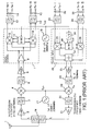
- FIG. 1 shows an example of conventional configuration that adopts a single super-heterodyne system as a configuration of a receiver.
- duplexer 16 for separating a transmission signal and a reception signal is connected to antenna 1.
- Low noise amplifier (LNA) 2, band-pass filter 3 for removing an image frequency signal, mixer 4, band-pass filter 5 for intermediate frequency (IF) and variable gain amplifier (VGA) 6 are connected in series in this order to the output of duplexer 16 for a reception signal, and an output of variable gain amplifier 6 is supplied to quadrature demodulator 7.
- the transceiver includes first local oscillator 17 for generating a first local signal and second local oscillator 18 for generating a second local signal. The first local signal is supplied to mixer 4.
- Quadrature demodulator 7 includes an amplifier 8 for amplifying an input signal to quadrature demodulator 7, a phase separation circuit 11 for receiving the second local signal as an input thereto and generating an in-phase (I) component and a quadrature (Q) component whose phase is displaced by 90 degrees (i.e., ⁇ /2) from that of the in-phase component, a multiplier 9 for multiplying an output of amplifier 8 and the in-phase component from phase separation circuit 11, and a multiplier 10 for multiplying the output of amplifier 8 and the quadrature component from phase separation circuit 11.
- ⁇ is, of course, the ratio of circumference of circle to its diameter.
- An output of multiplier 9 is supplied as reception baseband I signal 14 to the outside through band-pass filter 12 for baseband.
- An output of multiplier 10 is supplied as reception baseband Q signal 15 to the outside through band-pass filter 13 for baseband.
- a quadrature modulator 26 a variable gain amplifier 25 for intermediate frequency, a band-pass filter 24 for the intermediate frequency, a mixer 23, a band-pass filter 22 for removing image components and a power amplifier (PA) 21 are connected in series in this order.
- An output of power amplifier 21 is supplied to a terminal for a transmission signal of duplexer 16.
- Transmission baseband I signal 35 is supplied to quadrature modulator 26 through a band-pass filter 33 for a baseband, and also transmission baseband Q signal 36 is supplied to quadrature modulator 26 through a band-pass filter 34 for baseband.
- Quadrature modulator 26 includes a frequency divider 31 for dividing the frequency of the second local signal from second local oscillator 18 by 2 to produce a third local signal, a phase separation circuit 30 for receiving an output of frequency divider 31 as an input thereto and generating an in-phase (I) component and a quadrature (Q) component whose phase is displaced by 90 degrees ( ⁇ /2) from that of the in-phase component, a multiplier 29 for multiplying an output of band-pass filter 33 and the in-phase component from phase separation circuit 30, a multiplier 28 for multiplying an output of band-pass filter 34 and the quadrature component from phase separation circuit 30, and an adder 27 for adding outputs of multiplier 28 and multiplier 29 and outputting a result of the addition as an output of quadrature modulator 26.
- the transmission baseband I signal has a peak value of a component whose phase is the same as that of the third local signal
- the transmission baseband Q signal has a peak value of a component having a quadrature phase to that of the third local
- a reception signal is received by antenna 1 and separated by duplexer 16 which removes a transmission signal component from the reception signal.
- the separated reception signal is amplified by low noise amplifier 2 and inputted to band-pass filter 3 for removing the image component.
- the image component is a frequency component at a symmetrical position on the frequency axis to the reception signal with respect to the local frequency.
- the image component must be removed sufficiently by band-pass filter 3 because it otherwise leaks into the frequency band same as that of the signal when the signal is down converted by mixer 4.
- the reception signal from which the image component has been removed is mixed with the first local signal and down converted by mixer 4 to produce a reception intermediate frequency signal.
- first local frequency f LO1 ( ⁇ f t - f s ) 1,730 MHz to 1,790 MHz.
- the intermediate frequency signal is subjected to band-limitation by band-pass filter 5 and then amplified to a level necessary for quadrature demodulation by variable gain amplifier 6.
- the amplified signal is subjected to quadrature demodulation by quadrature demodulator 7 with the second local signal to produce a set of two reception baseband signals of an in-phase component (reception baseband I signal) and a quadrature component (reception baseband Q signal).
- phase separation circuit 11 In the inside of quadrature demodulator 7, phase separation circuit 11 generates an in-phase component and a quadrature component using the second local signal, and the in-phase component and the quadrature component are multiplied by the intermediate frequency signal by multipliers 9, 10 to generate respective reception baseband signals.
- reception baseband signals are subjected to band-limitation by band-pass filters 12, 13 and sent as reception baseband I signal 14, reception baseband Q signal 15, respectively, to a signal processing circuit (not shown) in the following stage so that data decoding of the reception signal is performed by the signal processing circuit.
- the frequency configuration of the reception side is associated closely with the configuration of the transmission side, and therefore, also operation of the transmission side will be described.
- a set of transmission baseband I signal 35 and transmission baseband Q signal 36 which are baseband signals produced by processing transmission data by means of a signal processing circuit (not shown) in the preceding stage are inputted and passed though band-pass filters 33, 34 for transmission baseband.
- Band-pass filters 33, 34 limit the frequency band of transmission baseband I signal 35 and transmission baseband Q signal 36, respectively.
- the band-limited transmission baseband signals are inputted to quadrature modulator 26 in which the quadrature modulation of those signals is performed.
- phase separation circuit 30 uses the third local signal to generate an in-phase component and a quadrature component. The in-phase component and the quadrature component are multiplied by the transmission baseband I signal and the transmission baseband Q signal by multipliers 29, 28, respectively, and resulting signals are added by adder 27 to generate a transmission intermediate frequency signal.
- the transmission intermediate frequency signal is amplified to a necessary level by variable gain amplifier 25 and then, after unnecessary waves outside the transmission band are removed from the transmission intermediate frequency by band-pass filter 24, it is supplied to mixer 23.
- Mixer 23 mixes the first local frequency and the transmission intermediate frequency signal to effect up conversion of the transmission intermediate frequency signal up to the transmission frequency band.
- First local frequency f LO1 is originally set to f LO1 ⁇ f t - f s , where f t is the transmission carrier frequency and f s is the transmission-reception carrier frequency interval, and apparently a correct transmission signal can be obtained if first local frequency f LO1 is added to central frequency f tm ⁇ f s of the transmission intermediate frequency to effect frequency conversion.
- the transmission signal produced by the up conversion by mixer 23 is supplied to band-pass filter 22, by which unnecessary waves outside the transmission frequency band such as an image frequency component generated inadvertently by mixer 23 are removed from the transmission signal. Then, the transmission signal from band-pass filter 22 is amplified up to a predetermined transmission output level by power amplifier 21 and transmitted through duplexer 16 and antenna 1.
- first local frequency f LO1 and second local frequency f LO2 are set in such a manner as described above, only two local oscillators 17, 18 can be used to generate all local signals necessary for transmission and reception. While the present specification uses the term “substantially” and the symbol “ ⁇ " when first local frequency f LO1 is set so as to be “substantially” equal to f t - f s , this is because, as obvious to those skilled in the art, it is not necessary to set f LO1 accurately to f t - f s and, in order to adjust the frequency to a prescribed transmission frequency band or reception frequency band, strictly the frequency band of the baseband signal itself must be taken into consideration. Therefore, in the present specification, displacement of the frequency is permitted as far as modulation, demodulation and frequency conversion can be performed in accordance with the scheme recited in the present specification.
- the conventional configuration which uses the single super-heterodyne system is such as described above. Although the conventional configuration operates sufficiently, it has the following problems if it is intended to proceed with development of an LSI (large scale integration) in order to reduce the cost and the number of parts of a radio unit in the future.
- LSI large scale integration
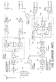
- FIG. 2 is a block diagram showing a configuration of a transceiver which adopts direct conversion for the reception side.
- the transceiver shown in FIG. 2 has a modified configuration to the transceiver shown in FIG. 1 in that it does not include mixer 4, band-pass filter 5 for intermediate frequency and variable gain amplifier 6 for intermediate frequency but instead includes variable gain amplifiers 19, 20 provided on the output side of band-pass filters 12, 13 for baseband, respectively, and a reception signal having passed through band-pass filter 3 for removing an image frequency component is inputted as it is to quadrature demodulator 7. Also, frequency f LO1 of the first local signal generated by first local oscillator 17 is different, and not the second local signal but the first local signal is supplied to phase separation circuit 11 of quadrature demodulator 7.
- the configuration of the transmission side and the configurations of second local oscillator 18, antenna 1, duplexer 16 and low noise amplifier 2 are same as those of the transceiver shown in FIG. 1. However, the frequency of the first local signal on the transmission side is different.
- the transceiver shown in FIG. 2 is different from that shown in FIG. 1 in that, after a reception signal passes through moderate band-pass filter 3, it is immediately converted into a reception baseband signal by quadrature demodulator 7.
- quadrature demodulator 7 uses the first local signal as a local signal for generation of a reception baseband signal.
- the first local signal is produced by first local oscillator 17 similarly as in the transceiver shown in FIG. 1.
- frequency f LO1 of the first local signal is substantially equal to reception carrier frequency f r .
- first local frequency f LO1 ( ⁇ f r ) 2,110 MHz to 2,170 MHz.
- quadrature demodulator 7 the first local signal is used to generate an in-phase component and a quadrature component by means of phase separation circuit 11, and the in-phase component and the quadrature component are multiplied by the reception signal by multipliers 9, 10, respectively, to generate reception baseband signals.
- the signals outputted from quadrature demodulator 7 have a peak value of a component of the reception signal which has a phase same as that of the internal local signal and a peak value of another component of the reception signal which has a quadrature phase to that of the internal local signal.
- reception baseband signals are subjected to band-limitation by band-pass filter 12, 13 for baseband and amplified to levels required for variable gain amplifiers 19, 20 and sent as reception baseband I signal 14 and reception baseband Q signal 15, respectively, to a signal processing circuit (not shown) in the following stage so that decoding of the reception data may be performed by the signal processing circuit.
- mixer 23 On the transmission side, the configuration itself is similar to that shown in FIG. 1. However, since frequency (first local frequency f LO1 ) of the first local signal is replaced by reception carrier frequency f r , mixer 23 operates in the following manner. In particular, since first local frequency f LO1 is substantially equal to f r and central frequency f tm of the transmission intermediate frequency signal is substantially equal to transmission-reception carrier frequency interval f s , mixer 23 extracts a frequency of the difference between them.
- an ordinary direct conversion receiver has problems in radiation of unnecessary waves to the outside of the apparatus by leak of a local signal, disturbance to a local oscillator by an intense reception signal from the outside and occurrence of a dc offset at an output of a quadrature demodulator by leak of a local signal into a reception signal.
- the configurations moderate such problems originating from interference between signals as described in paragraphs 4), 5), 6) above because a local oscillator which is influenced by an intense reception signal from the outside is not included on the inside of the receiver any more, and a printed wiring pattern through which a local signal having a frequency substantially equal to the reception carrier frequency passes is not included on the inside of the receiver any more.
- the present invention provides a means for making it possible to generate a local signal for demodulation on the inside of an LSI chip which includes a quadrature demodulator.
- a direct conversion receiver in order to allow reception of a radio frequency signal by direct conversion, comprises a first local oscillator for generating a first local signal of a first local frequency f LO1 ; a second local oscillator for generating a second local signal of a second local frequency f LO2 ; an internal local signal generator for mixing the first local signal and the second local signal to generate an internal local signal; and a quadrature demodulator for performing quadrature demodulation of the reception signal based on the internal local signal to generate the baseband signal.
- the first local frequency f LO1 satisfies f LO1 ⁇ f t + f s while the second local frequency f LO2 satisfies f LO2 ⁇ 2 ⁇ f s and the frequency of the internal local signal is a difference frequency between the first local frequency and the second local frequency.
- the receiver of the present invention having the configuration described above, although it is a receiver of the direct conversion system, it does not include a local oscillator having a frequency substantially equal to the reception carrier frequency any more, and consequently, the various problems arising from interference between a local signal and a reception signal are moderated significantly. Further, when the local signal used in the quadrature demodulator of the reception side is generated in an LSI chip which includes the quadrature demodulator, the various problems arising from interference between the local signal and a reception signal are moderated more significantly.
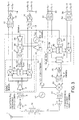
- FIG. 3 showing a transceiver (i.e., transmitter-receiver) of an embodiment of the present invention, components identical to those in FIGS. 1 and 2 are designated with the same reference numerals, and redundant description is not repeated therefor.
- the transceiver shown in FIG. 3 has a configuration substantially similar to that of the conventional transceiver shown in FIG. 2 but is different in the manner in which a local signal to be supplied to quadrature demodulator 7 is generated and the oscillation frequency (first local frequency) of first local oscillator 17.
- the transceiver shown in FIG. 3 in place of the configuration shown in FIG. 2 wherein the first local signal from first local oscillator 17 is supplied directly to phase separation circuit 11 in quadrature demodulator 7, the transceiver shown in FIG.
- buffer 40 for amplifying the first local signal
- buffer 39 for amplifying the second local signal from second local oscillator 18, mixer 38 for mixing an output of buffer 39 and an output of buffer 40
- band-pass filter 37 provided on the output side of mixer 38 for limiting the frequency band of the output of mixer 38.
- An output of band-pass filter 37 is supplied to phase separation circuit 11.
- the transceiver shown in FIG. 3 is quite the same as that shown in FIG. 2 in regard to the configuration of the transmission side and second local oscillator 18, antenna 1, duplexer 16, low noise amplifier 2, band-pass filter 3, quadrature demodulator 7, band-pass filters 12, 13 for baseband, variable gain amplifiers 19, 20 and so forth.
- reception carrier frequency f r is 2,110 MHz to 2,107 MHz
- transmission carrier frequency f t is 1,920 MHz to 1,980 MHz
- Frequency f LO1 of the first local signal generated by first local oscillator 17 in the transceiver shown in FIG. 3 is different from the frequency in the conventional transceiver of the direct conversion type shown in FIG. 2, but is rather similar to the frequency in the transceiver of the super-heterodyne type shown in FIG. 1.
- first local frequency f LO1 is substantially equal to f t - f s , that is, f LO1 ( ⁇ f t - f s ): 1,730 MHz to 1,790 MHz.
- first local frequency f LO1 is set in this manner and frequency f LO2 of the second local signal from second local oscillator 18 is 380 MHz and is the same as that in the cases shown in FIGS. 1 and 2, operation of the transmission side of the transceiver shown in FIG. 3 is quite the same as that of the transmission side of the conventional transceiver of the single super-heterodyne system shown in FIG. 1.
- the local signal used by quadrature demodulator 7 must have a frequency substantially equal to reception carrier frequency f r as long as the direct conversion is adopted.
- quadrature demodulator 7 is formed from an LSI (large scale integration) chip, if the local signal is generated outside the LSI chip, then such problems arising from interference between signals as described hereinabove appear. Therefore, in the present embodiment, the local signal for demodulation is generated in the following manner so that it can be generated in the inside of the LSI chip which includes quadrature demodulator 7 and besides the local signal need not be outputted to the outside of the LSI chip.
- This signal is extracted by band-pass filter 37 and used as a local signal for quadrature demodulator 7.
- band-pass filter 37 does not require a very steep cutoff characteristic, it need not be formed from a SAW filter or a dielectric filter. Accordingly, also band-pass filter 37 can be provided on the same LSI chip 50 as quadrature demodulator 7.
- Operation of the transceiver shown in FIG. 3 other than generation of the local signal used by quadrature demodulator 7 is similar to that of the conventional transceiver of the direct conversion system shown in FIG. 2.
- reception carrier frequency f r in the transceiver shown in FIG. 3 is higher than transmission carrier frequency f t
- the present invention is not limited to this.
- the present invention can be applied also when the arrangement of frequencies is reversed between the transmission side and the reception side, that is, even when f t > f r .
- FIG. 4 is a block diagram showing a configuration of a transceiver used when f t > f r .
- the transceiver shown in FIG. 4 has the quite same basic configuration as that shown in FIG. 3. However, since the frequency arrangement is reversed between the transmission side and the reception side, that is, reception carrier frequency f r and transmission carrier frequency f t are reverse in magnitude, oscillation frequency f LO1 of first local oscillator 17 is different from that shown in FIG. 3.
- Mixer 23 mixes the first local signal of first local frequency f LO1 and the transmission intermediate frequency signal to perform up conversion of the transmission intermediate frequency signal up to a transmission frequency band. Since first local frequency f LO1 originally is f LO1 ⁇ f t + f s' a transmission signal can be formed as a difference between first local frequency f LO1 and central frequency f tm of the transmission intermediate frequency.
- f LOINT internal local frequency f LOINT to be used in quadrature demodulator 7 of the reception side
- f LOINT is substantially equal to reception carrier frequency f r .
- the configuration of FIG. 4 is different from the configuration of FIG. 3 only in that the arrangement of frequencies is reversed between the transmission side and the reception side. Accordingly, the configuration of FIG. 4 is common in function and effect to the configuration of FIG. 3.
Landscapes
- Engineering & Computer Science (AREA)
- Physics & Mathematics (AREA)
- Electromagnetism (AREA)
- Power Engineering (AREA)
- Computer Networks & Wireless Communication (AREA)
- Signal Processing (AREA)
- Transceivers (AREA)
- Digital Transmission Methods That Use Modulated Carrier Waves (AREA)
- Superheterodyne Receivers (AREA)
Applications Claiming Priority (2)
| Application Number | Priority Date | Filing Date | Title |
|---|---|---|---|
| JP2000172449 | 2000-06-08 | ||
| JP2000172449A JP2001352355A (ja) | 2000-06-08 | 2000-06-08 | ダイレクトコンバージョン受信機及び送受信機 |
Publications (3)
| Publication Number | Publication Date |
|---|---|
| EP1162730A2 true EP1162730A2 (de) | 2001-12-12 |
| EP1162730A3 EP1162730A3 (de) | 2003-01-29 |
| EP1162730B1 EP1162730B1 (de) | 2007-07-25 |
Family
ID=18674849
Family Applications (1)
| Application Number | Title | Priority Date | Filing Date |
|---|---|---|---|
| EP20010250194 Expired - Lifetime EP1162730B1 (de) | 2000-06-08 | 2001-05-31 | Direktkonversion-Empfänger in einem Sender-Empfänger |
Country Status (6)
| Country | Link |
|---|---|
| US (1) | US7006814B2 (de) |
| EP (1) | EP1162730B1 (de) |
| JP (1) | JP2001352355A (de) |
| KR (1) | KR100404772B1 (de) |
| CN (1) | CN1174575C (de) |
| DE (1) | DE60129509T2 (de) |
Families Citing this family (13)
| Publication number | Priority date | Publication date | Assignee | Title |
|---|---|---|---|---|
| JP2005504476A (ja) * | 2001-09-19 | 2005-02-10 | シーメンス アクチエンゲゼルシヤフト | マルチバンド受信器および関連方法 |
| GB2382242B (en) * | 2001-11-15 | 2005-08-03 | Hitachi Ltd | Direct-conversion transmitting circuit and integrated transmitting/receiving circuit |
| US7224722B2 (en) * | 2002-01-18 | 2007-05-29 | Broadcom Corporation | Direct conversion RF transceiver with automatic frequency control |
| JP3908591B2 (ja) * | 2002-05-01 | 2007-04-25 | ソニー・エリクソン・モバイルコミュニケーションズ株式会社 | 変復調装置および携帯無線機 |
| US6952594B2 (en) * | 2002-11-22 | 2005-10-04 | Agilent Technologies, Inc. | Dual-mode RF communication device |
| US20060105726A1 (en) * | 2004-11-18 | 2006-05-18 | Tateo Masaki | Leakage electromagnetic wave communication device |
| US7495484B1 (en) * | 2007-07-30 | 2009-02-24 | General Instrument Corporation | Programmable frequency multiplier |
| JP5075189B2 (ja) * | 2009-12-03 | 2012-11-14 | 株式会社エヌ・ティ・ティ・ドコモ | 無線通信端末 |
| CN106301454A (zh) * | 2016-09-26 | 2017-01-04 | 武汉珞光电子有限公司 | 一种射频收发前端处理系统 |
| CN106487397A (zh) * | 2016-10-26 | 2017-03-08 | 上海华虹集成电路有限责任公司 | 发送电路 |
| CN106559377A (zh) * | 2016-10-26 | 2017-04-05 | 上海华虹集成电路有限责任公司 | 发送载波产生电路 |
| CN111866898B (zh) * | 2020-05-29 | 2025-08-05 | 郑思杰 | 无线通信信号分布系统及方法、移频器、接入和射频单元 |
| CN115065373B (zh) * | 2022-04-21 | 2023-12-12 | 海能达通信股份有限公司 | 多时隙收发信机和多时隙通信方法 |
Family Cites Families (19)
| Publication number | Priority date | Publication date | Assignee | Title |
|---|---|---|---|---|
| JPH01240020A (ja) | 1988-03-22 | 1989-09-25 | Alps Electric Co Ltd | 同時双方向fm送受信機 |
| US5170495A (en) * | 1990-10-31 | 1992-12-08 | Northern Telecom Limited | Controlling clipping in a microwave power amplifier |
| CA2107632C (en) * | 1992-10-05 | 1997-06-03 | Nec Corporation | Local oscillator and its frequency switching method |
| JPH06188781A (ja) | 1992-12-21 | 1994-07-08 | Toshiba Corp | デュアルモード無線通信装置 |
| DE4328553A1 (de) | 1993-04-30 | 1994-11-03 | Rudolf Prof Dr Ing Schwarte | Entfernungsmeßgerät nach dem Laufzeitprinzip |
| JP3410776B2 (ja) * | 1993-09-09 | 2003-05-26 | 株式会社東芝 | 直交信号発生回路 |
| US5412351A (en) * | 1993-10-07 | 1995-05-02 | Nystrom; Christian | Quadrature local oscillator network |
| DE4439298A1 (de) | 1994-11-07 | 1996-06-13 | Rudolf Prof Dr Ing Schwarte | 3D-Kamera nach Laufzeitverfahren |
| JPH0918528A (ja) * | 1995-06-27 | 1997-01-17 | Sony Corp | 制御信号検出方法及び無線受信装置 |
| JP3479405B2 (ja) * | 1996-03-29 | 2003-12-15 | アルプス電気株式会社 | 送信機の増幅回路 |
| JP3708234B2 (ja) | 1996-07-18 | 2005-10-19 | 松下電器産業株式会社 | 無線装置 |
| DE19704496C2 (de) | 1996-09-05 | 2001-02-15 | Rudolf Schwarte | Verfahren und Vorrichtung zur Bestimmung der Phasen- und/oder Amplitudeninformation einer elektromagnetischen Welle |
| JP3422909B2 (ja) | 1997-07-15 | 2003-07-07 | 株式会社東芝 | 無線機 |
| US5861781A (en) * | 1997-09-16 | 1999-01-19 | Lucent Technologies Inc. | Single sideband double quadrature modulator |
| US6016422A (en) * | 1997-10-31 | 2000-01-18 | Motorola, Inc. | Method of and apparatus for generating radio frequency quadrature LO signals for direct conversion transceivers |
| DE19821974B4 (de) | 1998-05-18 | 2008-04-10 | Schwarte, Rudolf, Prof. Dr.-Ing. | Vorrichtung und Verfahren zur Erfassung von Phase und Amplitude elektromagnetischer Wellen |
| CN1192498C (zh) * | 1999-03-01 | 2005-03-09 | 三菱电机株式会社 | 收发信装置 |
| JP2001230695A (ja) | 2000-02-16 | 2001-08-24 | Nec Corp | 無線機及びそれに使用する周波数変換方法 |
| US6782249B1 (en) * | 2000-11-22 | 2004-08-24 | Intel Corporation | Quadrature signal generation in an integrated direct conversion radio receiver |
-
2000
- 2000-06-08 JP JP2000172449A patent/JP2001352355A/ja active Pending
-
2001
- 2001-05-31 EP EP20010250194 patent/EP1162730B1/de not_active Expired - Lifetime
- 2001-05-31 DE DE2001629509 patent/DE60129509T2/de not_active Expired - Lifetime
- 2001-06-08 KR KR10-2001-0032095A patent/KR100404772B1/ko not_active Expired - Fee Related
- 2001-06-08 US US09/876,135 patent/US7006814B2/en not_active Expired - Fee Related
- 2001-06-08 CN CNB011231912A patent/CN1174575C/zh not_active Expired - Fee Related
Also Published As
| Publication number | Publication date |
|---|---|
| JP2001352355A (ja) | 2001-12-21 |
| EP1162730A3 (de) | 2003-01-29 |
| KR20010111051A (ko) | 2001-12-15 |
| DE60129509D1 (de) | 2007-09-06 |
| CN1174575C (zh) | 2004-11-03 |
| CN1328388A (zh) | 2001-12-26 |
| KR100404772B1 (ko) | 2003-11-07 |
| DE60129509T2 (de) | 2008-04-17 |
| US7006814B2 (en) | 2006-02-28 |
| EP1162730B1 (de) | 2007-07-25 |
| US20010051507A1 (en) | 2001-12-13 |
Similar Documents
| Publication | Publication Date | Title |
|---|---|---|
| US6600911B1 (en) | Even harmonic direct-conversion receiver, and a transmitting and receiving apparatus using the same | |
| US7006814B2 (en) | Direct conversion receiver and transceiver | |
| JPH0486139A (ja) | ダイレクトコンバージョン受信機 | |
| US6449471B1 (en) | Wireless terminal device | |
| JPH063886B2 (ja) | 折り返し試験機 | |
| JP2917890B2 (ja) | 無線送受信機 | |
| JPH06291697A (ja) | 送受信装置 | |
| JPH08331005A (ja) | 送受信機 | |
| US7039371B2 (en) | Transmitting device limiting the out-of-band interferences | |
| KR19990014666A (ko) | Rf 송신기 집적 회로에서의 스퓨리어스 신호 저감 | |
| US20100098134A1 (en) | Method and apparatus for using a spread spectrum intermediate frequency channel within an electronic device | |
| EP1089446A1 (de) | Funkendgerät | |
| JPH07321686A (ja) | ダイレクトコンバージョン受信機 | |
| JP3276856B2 (ja) | 無線送受信装置 | |
| JPH07303059A (ja) | 無線機 | |
| KR19990078141A (ko) | 무선장치 | |
| CN119341592A (zh) | Fdd通讯收发电路及收发器 | |
| KR100249676B1 (ko) | 국부 발진신호의 누설 신호 소거장치 | |
| JPH0629947A (ja) | スペクトラム拡散信号受信用相関回路ユニット | |
| JPH11313116A (ja) | 通信装置 | |
| JP2000101660A (ja) | 通信装置 | |
| JPH11136151A (ja) | 受信機および送受信機 | |
| JPH1146153A (ja) | ダイレクトコンバージョン方式の無線受信機 | |
| JPH06164553A (ja) | 周波数ダイバーシティ通信装置 | |
| JP2007028303A (ja) | 周波数変換装置 |
Legal Events
| Date | Code | Title | Description |
|---|---|---|---|
| PUAI | Public reference made under article 153(3) epc to a published international application that has entered the european phase |
Free format text: ORIGINAL CODE: 0009012 |
|
| AK | Designated contracting states |
Kind code of ref document: A2 Designated state(s): AT BE CH CY DE DK ES FI FR GB GR IE IT LI LU MC NL PT SE TR |
|
| AX | Request for extension of the european patent |
Free format text: AL;LT;LV;MK;RO;SI |
|
| PUAL | Search report despatched |
Free format text: ORIGINAL CODE: 0009013 |
|
| AK | Designated contracting states |
Designated state(s): AT BE CH CY DE DK ES FI FR GB GR IE IT LI LU MC NL PT SE TR |
|
| AX | Request for extension of the european patent |
Extension state: AL LT LV MK RO SI |
|
| 17P | Request for examination filed |
Effective date: 20030210 |
|
| AKX | Designation fees paid |
Designated state(s): DE FR GB IT |
|
| PUAF | Information related to the publication of a search report (a3 document) modified or deleted |
Free format text: ORIGINAL CODE: 0009199SEPU |
|
| PUAL | Search report despatched |
Free format text: ORIGINAL CODE: 0009013 |
|
| D17D | Deferred search report published (deleted) | ||
| AK | Designated contracting states |
Kind code of ref document: A3 Designated state(s): DE FR GB IT |
|
| GRAP | Despatch of communication of intention to grant a patent |
Free format text: ORIGINAL CODE: EPIDOSNIGR1 |
|
| GRAS | Grant fee paid |
Free format text: ORIGINAL CODE: EPIDOSNIGR3 |
|
| GRAA | (expected) grant |
Free format text: ORIGINAL CODE: 0009210 |
|
| AK | Designated contracting states |
Kind code of ref document: B1 Designated state(s): DE FR GB IT |
|
| REG | Reference to a national code |
Ref country code: GB Ref legal event code: FG4D |
|
| REF | Corresponds to: |
Ref document number: 60129509 Country of ref document: DE Date of ref document: 20070906 Kind code of ref document: P |
|
| ET | Fr: translation filed | ||
| PLBE | No opposition filed within time limit |
Free format text: ORIGINAL CODE: 0009261 |
|
| STAA | Information on the status of an ep patent application or granted ep patent |
Free format text: STATUS: NO OPPOSITION FILED WITHIN TIME LIMIT |
|
| 26N | No opposition filed |
Effective date: 20080428 |
|
| PG25 | Lapsed in a contracting state [announced via postgrant information from national office to epo] |
Ref country code: IT Free format text: LAPSE BECAUSE OF NON-PAYMENT OF DUE FEES Effective date: 20080531 |
|
| PGFP | Annual fee paid to national office [announced via postgrant information from national office to epo] |
Ref country code: GB Payment date: 20140528 Year of fee payment: 14 |
|
| PGFP | Annual fee paid to national office [announced via postgrant information from national office to epo] |
Ref country code: FR Payment date: 20140509 Year of fee payment: 14 Ref country code: DE Payment date: 20140528 Year of fee payment: 14 |
|
| REG | Reference to a national code |
Ref country code: DE Ref legal event code: R119 Ref document number: 60129509 Country of ref document: DE |
|
| GBPC | Gb: european patent ceased through non-payment of renewal fee |
Effective date: 20150531 |
|
| REG | Reference to a national code |
Ref country code: FR Ref legal event code: ST Effective date: 20160129 |
|
| PG25 | Lapsed in a contracting state [announced via postgrant information from national office to epo] |
Ref country code: GB Free format text: LAPSE BECAUSE OF NON-PAYMENT OF DUE FEES Effective date: 20150531 Ref country code: DE Free format text: LAPSE BECAUSE OF NON-PAYMENT OF DUE FEES Effective date: 20151201 |
|
| PG25 | Lapsed in a contracting state [announced via postgrant information from national office to epo] |
Ref country code: FR Free format text: LAPSE BECAUSE OF NON-PAYMENT OF DUE FEES Effective date: 20150601 |