EP1163640B1 - Dispositif et methode pour convertir des chaines de bits - Google Patents
Dispositif et methode pour convertir des chaines de bits Download PDFInfo
- Publication number
- EP1163640B1 EP1163640B1 EP00909630A EP00909630A EP1163640B1 EP 1163640 B1 EP1163640 B1 EP 1163640B1 EP 00909630 A EP00909630 A EP 00909630A EP 00909630 A EP00909630 A EP 00909630A EP 1163640 B1 EP1163640 B1 EP 1163640B1
- Authority
- EP
- European Patent Office
- Prior art keywords
- output
- storing
- bit
- register
- conversion
- Prior art date
- Legal status (The legal status is an assumption and is not a legal conclusion. Google has not performed a legal analysis and makes no representation as to the accuracy of the status listed.)
- Expired - Lifetime
Links
Images
Classifications
-
- G—PHYSICS
- G06—COMPUTING OR CALCULATING; COUNTING
- G06T—IMAGE DATA PROCESSING OR GENERATION, IN GENERAL
- G06T3/00—Geometric image transformations in the plane of the image
- G06T3/40—Scaling of whole images or parts thereof, e.g. expanding or contracting
Definitions
- This invention relates to a device for converting bit strings comprising first control means, first storing means connected to the first control means and suitable for storing first strings of bits representative of source information to be converted, second storing means connected to the first control means and to the first storing means and suitable for storing second strings of bits representative of converted information.
- this invention relates to a device and relative method of converting information representing images from one resolution to another.
- the peripheral units connected to an electronic processor such as for instance printers, facsimile machines, scanners, use resolutions that may differ from one peripheral to another or even on the same peripheral.
- a monofunctional peripheral for instance an ink jet printer, can print with different resolutions, such as 150, 300, 600 dots per inch (or d.p.i.), where 1 inch corresponds in metric terms to about 25.4 mm, whereas a facsimile machine and a scanner may perform the scanning of a document with a resolution of 200 d.p.i. and transfer the information thus generated to the processor or to the printer itself according to resolution different from that of scanning.
- integrated peripherals are commercially available that are capable of performing various functions, for instance printer, scanner and facsimile functions. Both the monofunctional and the integrated peripherals are capable, where necessary, of converting information from one resolution to another, but require an exceptionally high processing commitment and times of the central processing unit (CPU).
- CPU central processing unit
- the CPU of these peripherals uses predefined programs (software) intended for the manipulation of single data bits, an operation which, as will be obvious to those acquainted with the sector art, requires a large number of elementary instructions and accordingly high processing times.
- predefined programs software intended for the manipulation of single data bits
- the simple implementation in a printer of an algorithm for conversion from a resolution of 150 d.p.i. to one of 300 d.p.i. requires that each single bit of source data be duplicated; in this operation, assuming a CPU with a normal instruction set, the CPU is required to load a string of the source information bits in an accumulator and, for each bit of this string, to store the same duplicated bit in a second accumulator.
- the CPU will require a total of 16 clock pulses to duplicate each single bit.
- the conversion times for single bits of information are long and necessarily depend both on the CPU, i.e. its instruction set, and on the clock rate.
- the technical problem that this invention intends to solve is that of drastically reducing, by a factor of 100 or even more, the times needed by the monofunctional or integrated peripherals to perform the conversion of single data bits, for example in the conversions from one resolution to another, without having recourse, as happens in the known art, to the use of high speed CPUs or those with special instruction sets.
- the invention intends to solve this problem by separating the data conversion functions from the characteristics of the CPU and its clock.
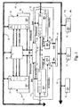
- the device comprises a central processing unit (CPU) 11, of known type, a read only memory (ROM) 12, known in its own right, suitable for memorizing data and programs developed in the device's design stage and a random access memory (RAM) 14, suitable for memorizing the information on which to perform the conversion.
- the RAM 14, of known type comprises a first zone 14a suitable for storing the information to be converted or source information, and a second zone 14b suitable for storing the converted information or output information.
- the CPU 11, the ROM 12 and the RAM 14 are connected to each other in a known way by means of a data and address channel (or bus) 15 and are timed, in accordance with this embodiment, at a first clock rate (clk1).
- the device also comprises a first and a second control register, 21 and 22 respectively, and a multiplexer circuit 23, all of known type, connected to the bus 15.
- the control registers 21 and 22 are, for example, 32-bit shift registers and are suitable for storing strings of bits of variable length, up to a maximum of 32 bits, representing the type of conversion to be effected, as will be described later in detail and, in accordance with this embodiment, are suitable for having a "shift" at a second clock rate (clk2), two or more times greater than clk1.
- the storing of the control registers 21 and 22 is effected by the CPU 11 which, in relation to the type of conversion to be performed, is adapted for reading from the ROM 12 a pair of predefined bit strings of equal length and for storing them in the control registers 21 and 22 by means of the bus 15.
- the multiplexer 23 is connected to the control registers 21 and 22, and is suitable for enabling the "shifting" of the control registers 21 and 22 by up to the predefined length of the pair of bit strings stored in the same control registers 21 and 22, in relation to the predefined data stored in the ROM 12 and transmitted by the CPU 11 to the multiplexer 23 by means of the bus 15.
- the device finally comprises an encoder circuit 25, an input shift register 31, an output shift register 32, a first and a second counter, 36 and 37, associated respectively with the input register 31 and the output register 32, and a status register 35.
- the encoder 25, of known type has a first and a second input connected respectively to the first and the second control register 21 and 22, a first output 33 connected to the input register 31 and to the corresponding counter 36 and a second output 34 connected to the output register 32 and to the corresponding counter 37.
- the encoder 25 is suitable for commanding the selective shifting of the input register 31 and of the associated counter 36 and/or of the output register 32 and of the associated counter 37, in relation to the binary configuration of the single pairs of bits input to the encoder 25 itself by the pair of control registers 21 and 22 cooperating with each other.
- the encoder 25 is suitable for generating on the first output (wire) 33 a signal "ENSHSORG” to command the shifting of the input register 31 and relative counter 36, and/or on the second output (wire) 34 a signal "ENSHDEST" to command the shifting of the output register 32 and relative counter 37, in accordance with the following truth table.
- the encoder 25 is also connected, by means of a third output 24, to the control registers 21 and 22, and is adapted for controlling their shifting by sending an enable signal "ENSHMASK" to this third output 24 in parallel with the selective activation of the input register 31 and/or of the output register 32.
- the input register 31, for example a 16-bit shift register of known type, has a data input connected to the bus 15, a data output connected to the output register 32, a control output 38 connected to the first counter 36 and is timed, with regard to the shifting, in accordance with clk2.
- the input register 31 is suitable for receiving and storing, through the bus 15 and under the control of the CPU 11, a string of source information, read from the zone 14a of the RAM 14 and for transmitting, in parallel, by means of the control output 38, a signal "CLRIBE" to the counter 36.
- the input register 31 is also suitable for performing the shifting of a bit depending on whether signal "ENSHSORG” is present on the wire 33 and for transferring a bit to the output register 32 during the shifting.
- the output register 32 for example a 16-bit shift register of known type, has a data output connected to the bus 15 and a control output 39 connected to the second counter 37, and is timed, with regard to the shifting, in accordance with clk2.
- the output register 32 is suitable for transferring, under the control of the CPU 11, strings of output information into the zone 14b of the RAM 14 and for transmitting, in parallel, by means of the control output 39, a signal "CLROBF" to the counter 37.
- the output register 32 is also suitable for performing the shifting by 1 bit, depending on whether the control signal "ENSHDEST" is present on the wire 34.
- the first counter 36 for example a counter by 16 of known type, has a control output (first counter output) 41 connected to the status register 35 and to the encoder 25, and is suitable for generating a buffer empty signal (flag) "IBE” once the shifting of the input register 31 is complete (reading of the source information string) and for lowering this flag when signal "CLRIBE” is present.
- the second counter 37 for example a 16-bit counter of known type, has a control output (second counter output) 42 connected to the status register 35 and to the encoder 25, and is suitable for generating a buffer full signal (flag) "OBF” once the shifting of the output register 32 is complete (writing of the output information string) and for lowering this flag when signal "CLROBF" is present.
- the status register 35 of known type, is connected to the bus 15 and is suitable for being selected and read by the CPU 11 for detecting the presence of flag "IBE" and/or "OBF".
- the CPU 11 reads from the ROM 12 the pair of bit strings corresponding to the conversion algorithm to be performed and stores it by means of the bus 15 in the control registers 21 and 22. Furthermore the CPU 11, depending on the length of these bit strings, presets the multiplexer 23 in such a way as to constrain the reading of the control registers 21 and 22 in rotation in accordance with the length of the pair of bit strings. Finally, the CPU 11 commands the reading from the first zone 14a of the RAM 14 of a first string of source information to be converted and stores it in the input register 31 which, in turn, resets the first counter 36 by means of the control wire 38.
- the device can effect the conversion selected at the rate clk2 without any further intervention of the CPU 11.
- the control registers 21 and 22 will contain, for example, the following strings of 18 bits: Reg. 21 1 0 0 1 0 0 1 0 0 1 0 0 1 0 0 1 0 0 1 0 0 0 Reg. 22 0 1 1 0 1 1 0 1 1 0 1 1 0 1 1 0 1 1 1 1 1 1 1 1 1 1 1 1 1 1 1 1 1 1 1 1 1 1 1 1 1 1 1 1 1 1 1 1 1 1 1 1 1 1 1 1 1 1 1 1 1 1 1 1 1 1 1 1 1 1 1 1 1 1 1 1 1 1 1 1 1 1 1 1 1 1 1 1 1 1 1 1 1 1 1 1 1 1 1 1 1 1 1 1 1 1 1 1 1 1 1 1 1 1 1 1 1 1 1 1 1 1 1 1 1 1 1 1 1 1 1 1 1 1 1 1 1 1 1 1 1 1 1 1 1 1 1 1 1 1 1 1 1 1 1 1 1 1 1
- the first binary configuration "1 0" is transmitted to the encoder 25 which generates as output, in accordance with the truth table described, the signals "ENSHSORG” and “ENSHDEST” with consequent shifting of the input and output registers, 31 and 32, and copying of a bit from the input register 31 to the output register 32.
- the second binary configuration "0 1” is transmitted to the encoder 25 which generates as output signal "ENSHDEST” only, with consequent shifting of only the output register 32 and duplication of the bit present on the output by the input register 31 .
- the third binary configuration "0 1", identical to the second one, is transmitted to the encoder 25 which generates as output signal "ENSHDEST" only, with consequent shifting of only the output register 32 and duplication or expansion of the bit present on the output by the input register 31.
- the fourth clock pulse clk2 what was described for the first clock pulse clk2 is repeated, and so on.
- the conversion of the example involves the output register 32 completing the first shifting before the input register 31 and accordingly the second counter 37 completing its count first.
- the second counter 37 at the end of the count, generates as output the flag "OBF” (output buffer full) and transmits it to the status register 35 and to the encoder 25 by means of the control output 42.
- the encoder 25 On receiving the flag "OBF” the encoder 25 stops the conversion process by holding the registers 21, 22, 31, 32 and the counters 36, 37 blocked for as long as the flag "OBF” is raised, whereas the CPU 11, once the flag "OBF" is intercepted, reads the contents from the output register 32 and stores them, by means of the bus 15, in the second zone 14b of the RAM 14.
- the output register 32 sends the counter 37, by means of the control wire 39, the signal "CLROBF" and the counter 37 lowers the flag "OBF” permitting the encoder 25 to release the conversion process.
- control registers 21 and 22 will, for example, contain the following strings of 18 bits: Reg. 21 1 0 0 1 0 0 1 0 0 1 0 0 1 0 0 1 0 0 1 0 0 0 Reg. 22 0 0 0 0 0 0 0 0 0 0 0 0 0 0 0 0 0 0 0 0 0 0 0 0 0 0 0 0 0 0 0 0 0 0 0 0 0 0 0 0 0 0 0 0 0 0 0 0 0 0 0 0 0 0 0 0 0 0 0 0 0 0 0 0 0 0 0 0 0 0 0 0 0 0 0 0 0 0 0 0 0 0 0 0 0 0 0 0 0 0 0 0 0 0 0 0
- the first binary configuration "1 0" is transmitted to the encoder 25 which generates as output, in accordance with the truth table, the signals "ENSHSORG” and “ENSHDEST” with consequent copying of a bit from the input register 31 to the output register 32.
- the second binary configuration "0 0” is transmitted to the encoder 25 which generates as output signal "ENSHSORG", only with consequent shifting of only the input register 31 and loss (compression) of the bit transmitted in output by the input register 31.
- the third binary configuration "0 0" is transmitted to the encoder 25 which generates as output signal "ENSHSORG" only, with consequent shifting of only the input register 31 and loss of the bit transmitted in output by the input register 31.
- the fourth clock pulse clk2 what was described for the first clock pulse is repeated, and so on.
- the conversion involves the input register 31 completing the first shifting before the output register 32 and accordingly the first counter 36 completing its count first.
- the first counter 36 at the end of the count generates as output the flag "IBE" (input buffer empty) and transmits it to the status register 35 and to the encoder 25 by means of the control output 41.
- the encoder 25 On reception of the flag "IBE” the encoder 25 stops the conversion process by holding the registers 21, 22, 31, 32 and the counters 36, 37 blocked for as long as the flag "IBE” is raised.
- the device according to the invention permits the implementation of any conversion algorithm, either through the definition of pairs of bit strings of length variable with the variation of the algorithm or through the definition of a truth table comprising at least three basic functions, such as copying, expansion and compression of single bits.
- the speed of conversion depends solely on the shifting speed of the registers 21, 22, 31 and 32 and of the counters 36 and 36, as the CPU 11 only intervenes in the conversion process in the step of writing the source information in the input register 31 or in the step of reading the output information from the output register 32, depending on whether the flag "IBE" and/or "OBF" is present in the status register 35. Furthermore, in the steps of writing and reading the CPU 11 works on strings of source and output information, and not on the single bits.
- truth table may be defined differently and the encoder 25 can operate in accordance with truth tables having different binary configurations, without departing from the scope of the invention.
- control registers 21 and 22, of the input and output registers 31 and 32, and of the counters 36 and 37 may be different from that described in the present embodiment, again without departing from the scope of the invention. Changes may be made to the dimensions, shapes, materials, components, circuit elements, connections and contacts, as also to the circuitry and construction details illustrated and to the method of operation without departing from the scope of the invention as defined in the appended claims.
Landscapes
- Physics & Mathematics (AREA)
- General Physics & Mathematics (AREA)
- Engineering & Computer Science (AREA)
- Theoretical Computer Science (AREA)
- Compression, Expansion, Code Conversion, And Decoders (AREA)
- Transmission And Conversion Of Sensor Element Output (AREA)
- Communication Control (AREA)
- Image Processing (AREA)
- Editing Of Facsimile Originals (AREA)
Claims (6)
- Dispositif de conversion de chaínes de bits comprenantcaractérisé parun premier moyen de commande (11);un premier moyen de mise en mémoire (31) relié audit premier moyen de commande (11) pour mettre en mémoire des premières chaínes de bits représentant des informations sources à convertir ;un second moyen de mise en mémoire (32) relié audit premier moyen de commande (11) et audit premier moyen de mise en mémoire (31) pour mettre en mémoire des secondes chaínes de bits représentant des informations converties ;un second moyen de commande (21, 22, 25) comprenant un nombre prédéfini de configurations binaires, chacune représentant un algorithme de conversion, relié auxdits premier (31) et second (32) moyens de mise en mémoire pour commander par l'intermédiaire desdites configurations binaires la conversion de chaque bit desdites informations sources auxdites informations converties ; dans lequelledit premier moyen de commande (11) est cadencé à une première fréquence d'horloge (clk1) et ledit premier moyen de mise en mémoire (31), ledit second moyen de mise en mémoire (32) et ledit second moyen de commande (21, 22, 25) sont cadencés à une fréquence d'horloge prédéfinie (clk2) différente de celle dudit premier moyen de commande (11).
- Dispositif selon la revendication 1, caractérisé en ce que lesdites configurations binaires sont composées de paires de bits.
- Dispositif selon la revendication 2, caractérisé en ce que lesdites paires de bits comprennent au moins trois configurations différentes.
- Dispositif selon la revendication 1 ou 2, caractérisé en ce que ledit second moyen de commande (21, 22, 25) comprendune paire de registres à décalage (21, 22) destinés à transmettre lesdites configurations binaires ; etun circuit codeur (25) relié à ladite paire de registres à décalage (21, 22) pour commander sélectivement ledit premier (31) et ledit second (32) moyens de mise en mémoire par rapport auxdites configurations binaires.
- Dispositif selon la revendication 4, caractérisé en ce quelesdits premier (31) et second (32) moyens de mise en mémoire comprennent chacun au moins un registre à décalage.
- Procédé de conversion de chaínes de bits comprenant les étapes consistant àmettre en mémoire à une première fréquence d'horloge (clk1) une chaíne de bits représentant des informations sources à convertir dans le premier moyen de mise en mémoire (31) ; caractérisé par les étapes consistant àappliquer à une seconde fréquence d'horloge (clk2) un algorithme de conversion à chaque bit de ladite première chaíne de bits ; etmettre en mémoire sélectivement chacun desdits bits dudit premier moyen de mise en mémoire (31) dans le second moyen de mise en mémoire (32) selon ladite seconde fréquence d'horloge et ledit algorithme de conversion afin de composer dans ledit second moyen de mise en mémoire (32) une seconde chaíne de bits représentant une chaíne d'informations converties.
Applications Claiming Priority (3)
| Application Number | Priority Date | Filing Date | Title |
|---|---|---|---|
| ITTO990175 | 1999-03-08 | ||
| IT1999TO000175A IT1308414B1 (it) | 1999-03-08 | 1999-03-08 | Dispositivo per la conversione di stringhe di bit |
| PCT/IT2000/000060 WO2000054218A1 (fr) | 1999-03-08 | 2000-02-25 | Dispositif pour convertir des chaînes de bits |
Publications (2)
| Publication Number | Publication Date |
|---|---|
| EP1163640A1 EP1163640A1 (fr) | 2001-12-19 |
| EP1163640B1 true EP1163640B1 (fr) | 2002-08-28 |
Family
ID=11417579
Family Applications (1)
| Application Number | Title | Priority Date | Filing Date |
|---|---|---|---|
| EP00909630A Expired - Lifetime EP1163640B1 (fr) | 1999-03-08 | 2000-02-25 | Dispositif et methode pour convertir des chaines de bits |
Country Status (5)
| Country | Link |
|---|---|
| US (1) | US6700577B1 (fr) |
| EP (1) | EP1163640B1 (fr) |
| DE (1) | DE60000367T2 (fr) |
| IT (1) | IT1308414B1 (fr) |
| WO (1) | WO2000054218A1 (fr) |
Families Citing this family (2)
| Publication number | Priority date | Publication date | Assignee | Title |
|---|---|---|---|---|
| TW200606811A (en) * | 2004-06-25 | 2006-02-16 | Ssd Co Ltd | Image mixing apparatus and pixel mixer |
| US10833700B2 (en) * | 2019-03-13 | 2020-11-10 | Micron Technology, Inc | Bit string conversion invoking bit strings having a particular data pattern |
Family Cites Families (4)
| Publication number | Priority date | Publication date | Assignee | Title |
|---|---|---|---|---|
| US4771279A (en) * | 1987-07-10 | 1988-09-13 | Silicon Graphics, Inc. | Dual clock shift register |
| JPH052643A (ja) * | 1991-06-25 | 1993-01-08 | Canon Inc | 画像処理装置 |
| EP0574901A2 (fr) * | 1992-06-16 | 1993-12-22 | Kabushiki Kaisha Toshiba | Processeur de signaux d'image |
| JPH0991415A (ja) * | 1995-09-26 | 1997-04-04 | Taito Corp | ラインズーム回路 |
-
1999
- 1999-03-08 IT IT1999TO000175A patent/IT1308414B1/it active
-
2000
- 2000-02-25 EP EP00909630A patent/EP1163640B1/fr not_active Expired - Lifetime
- 2000-02-25 WO PCT/IT2000/000060 patent/WO2000054218A1/fr not_active Ceased
- 2000-02-25 DE DE60000367T patent/DE60000367T2/de not_active Expired - Lifetime
- 2000-02-25 US US09/936,225 patent/US6700577B1/en not_active Expired - Lifetime
Also Published As
| Publication number | Publication date |
|---|---|
| DE60000367D1 (de) | 2002-10-02 |
| WO2000054218A1 (fr) | 2000-09-14 |
| EP1163640A1 (fr) | 2001-12-19 |
| ITTO990175A1 (it) | 2000-09-08 |
| IT1308414B1 (it) | 2001-12-17 |
| US6700577B1 (en) | 2004-03-02 |
| DE60000367T2 (de) | 2003-05-15 |
Similar Documents
| Publication | Publication Date | Title |
|---|---|---|
| JPH0145656B2 (fr) | ||
| EP1163640B1 (fr) | Dispositif et methode pour convertir des chaines de bits | |
| JP3552144B2 (ja) | 総合画像形成装置 | |
| US6980701B1 (en) | Image processing method and apparatus capable of rotating and reversing an input image | |
| JP2650416B2 (ja) | ラスタスキャン方式の両面印刷装置 | |
| JPH06284282A (ja) | 画像形成装置 | |
| JP3093218B2 (ja) | デジタル画像処理装置 | |
| JPH0563959A (ja) | 画像処理方法および装置 | |
| KR200146385Y1 (ko) | 버스 스위치를 이용한 이중 버스 구조의 잉크젯 프린터 시스템 | |
| JP4158575B2 (ja) | データ処理システム | |
| JP2955301B2 (ja) | 画像処理方法 | |
| JP2715475B2 (ja) | 図形出力装置 | |
| JPS6016757A (ja) | 文書伝送方式 | |
| JP2803560B2 (ja) | プリンタ制御装置 | |
| JP2001047677A (ja) | プリンタ制御装置 | |
| JP2908571B2 (ja) | ページプリンタ | |
| JPH0477971A (ja) | 画像処理装置 | |
| JPH05344298A (ja) | スキャナプリンタ | |
| JPS609792A (ja) | 印字装置 | |
| JPH0863594A (ja) | ディジタル画像処理用のメモリ制御装置 | |
| JPH066606A (ja) | 網点信号発生装置 | |
| JPH07152519A (ja) | 印刷システム | |
| JPH081990A (ja) | プリンタ | |
| JPH11284789A (ja) | 画像形成装置、画像処理装置、及び画像形成システム | |
| JPH047175A (ja) | ページプリンタ制御装置 |
Legal Events
| Date | Code | Title | Description |
|---|---|---|---|
| PUAI | Public reference made under article 153(3) epc to a published international application that has entered the european phase |
Free format text: ORIGINAL CODE: 0009012 |
|
| 17P | Request for examination filed |
Effective date: 20010920 |
|
| AK | Designated contracting states |
Kind code of ref document: A1 Designated state(s): AT BE CH CY DE DK ES FI FR GB GR IE IT LI LU MC NL PT SE |
|
| GRAG | Despatch of communication of intention to grant |
Free format text: ORIGINAL CODE: EPIDOS AGRA |
|
| GRAG | Despatch of communication of intention to grant |
Free format text: ORIGINAL CODE: EPIDOS AGRA |
|
| GRAH | Despatch of communication of intention to grant a patent |
Free format text: ORIGINAL CODE: EPIDOS IGRA |
|
| RTI1 | Title (correction) |
Free format text: BIT STRING CONVERSION DEVICE AND METHOD |
|
| RTI1 | Title (correction) |
Free format text: BIT STRING CONVERSION DEVICE AND METHOD |
|
| 17Q | First examination report despatched |
Effective date: 20020213 |
|
| GRAH | Despatch of communication of intention to grant a patent |
Free format text: ORIGINAL CODE: EPIDOS IGRA |
|
| GRAA | (expected) grant |
Free format text: ORIGINAL CODE: 0009210 |
|
| AK | Designated contracting states |
Kind code of ref document: B1 Designated state(s): DE FR GB |
|
| REG | Reference to a national code |
Ref country code: GB Ref legal event code: FG4D |
|
| REF | Corresponds to: |
Ref document number: 60000367 Country of ref document: DE Date of ref document: 20021002 |
|
| REG | Reference to a national code |
Ref country code: IE Ref legal event code: FG4D |
|
| ET | Fr: translation filed | ||
| PLBE | No opposition filed within time limit |
Free format text: ORIGINAL CODE: 0009261 |
|
| STAA | Information on the status of an ep patent application or granted ep patent |
Free format text: STATUS: NO OPPOSITION FILED WITHIN TIME LIMIT |
|
| 26N | No opposition filed |
Effective date: 20030530 |
|
| REG | Reference to a national code |
Ref country code: IE Ref legal event code: MM4A |
|
| REG | Reference to a national code |
Ref country code: FR Ref legal event code: PLFP Year of fee payment: 16 |
|
| PGFP | Annual fee paid to national office [announced via postgrant information from national office to epo] |
Ref country code: DE Payment date: 20150122 Year of fee payment: 16 |
|
| REG | Reference to a national code |
Ref country code: DE Ref legal event code: R082 Ref document number: 60000367 Country of ref document: DE Representative=s name: PATENTANWAELTE WEICKMANN & WEICKMANN, DE Ref country code: DE Ref legal event code: R082 Ref document number: 60000367 Country of ref document: DE Representative=s name: WEICKMANN & WEICKMANN PATENTANWAELTE - RECHTSA, DE |
|
| PGFP | Annual fee paid to national office [announced via postgrant information from national office to epo] |
Ref country code: GB Payment date: 20150123 Year of fee payment: 16 Ref country code: FR Payment date: 20150220 Year of fee payment: 16 |
|
| REG | Reference to a national code |
Ref country code: DE Ref legal event code: R119 Ref document number: 60000367 Country of ref document: DE |
|
| GBPC | Gb: european patent ceased through non-payment of renewal fee |
Effective date: 20160225 |
|
| REG | Reference to a national code |
Ref country code: FR Ref legal event code: ST Effective date: 20161028 |
|
| PG25 | Lapsed in a contracting state [announced via postgrant information from national office to epo] |
Ref country code: GB Free format text: LAPSE BECAUSE OF NON-PAYMENT OF DUE FEES Effective date: 20160225 Ref country code: FR Free format text: LAPSE BECAUSE OF NON-PAYMENT OF DUE FEES Effective date: 20160229 Ref country code: DE Free format text: LAPSE BECAUSE OF NON-PAYMENT OF DUE FEES Effective date: 20160901 |